TL F 10721
DS3885
BTL
Arbitration
Transceiver
January 1994
DS3885 BTL Arbitration Transceiver
General Description
The DS3885 is one in a series of transceivers designed spe-
cifically for the implementation of high performance Future-
bus
a
and proprietary bus interfaces The DS3885 Arbitra-
tion Transceiver is designed to conform to IEEE 1194 1
(Backplane Transceiver Logic
BTL) as specified in the
IEEE 896 2 Futurebus
a
specification
The Arbitration
Transceiver incorporates the competition logic internally
which simplifies the implementation of a Futurebus
a
appli-
cation by minimizing the on board logic required
The DS3885 driver output configuration is an NPN open col-
lector which allows Wired-OR connection on the bus Each
driver output incorporates a Schottky diode in series with its
collector to isolate the transistor output capacitance from
the bus thus reducing the bus loading in the inactive state
The BTL drivers also have high sink current capability to
comply with the bus loading requirements defined within
IEEE 1194 1 BTL specification
Backplane Transceiver Logic (BTL) is a signaling standard
that was invented and first introduced by National Semicon-
(Continued)
Features
Y
9-bit inverting BTL transceiver
Y
Meets IEEE 1194 1 standard on Backplane Transceiver
Logic (BTL)
Y
Includes on chip competition logic and parity checking
Y
Supports live insertion
Y
Glitch free power-up down protection
Y
Typically less than 5 pF bus-port capacitance
Y
Low bus-port voltage swing (typically 1V) at 80 mA
Y
Open collector bus-port output allows Wired-OR
connection
Y
Exceeds 2 kV ESD testing (Human Body Model)
Y
Individual bus-port ground pins minimize ground bounce
Y
Controlled rise and fall time to reduce noise coupling to
adjacent lines
Y
TTL compatible driver and control inputs
Y
Built in bandgap reference with separate QV
CC
and
QGND pins for precise receiver thresholds
Y
Product offered in PLCC and PQFP package styles
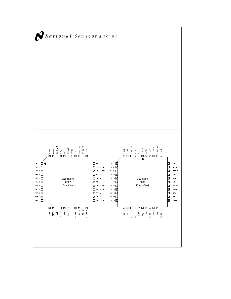
Connection Diagrams
TL F 10721 � 2
TL F 10721 � 13
Order Number DS3885V or DS3885VF
See NS Package Number V44A or VF44B
TRI-STATE
is a registered trademark of National Semiconductor Corporation
C1995 National Semiconductor Corporation
RRD-B30M75 Printed in U S A

General Description
(Continued)
ductor then developed by the IEEE to enhance the per-
formance of backplane buses BTL compatible transceivers
feature low output capacitance drivers to minimize bus load-
ing a 1V nominal signal swing for reduced power consump-
tion and receivers with precision thresholds for maximum
noise immunity BTL eliminates settling time delays that se-
verely limit TTL bus performance and thus provide signifi-
cantly higher bus transfer rates The backplane bus is in-
tended to be operated with termination resistors (selected
to match the bus impedance) connected to 2 1V at both
ends The low voltage is typically 1V
Separate ground pins are provided for each BTL output to
minimize induced ground noise during simultaneous switch-
ing
The transceiver's control and driver inputs are designed
with high impedance PNP input structures and are fully TTL
compatible
The receiver is a high speed comparator that utilizes a
bandgap reference for precision threshold control allowing
maximum noise immunity to the BTL 1V signaling level
Separate QV
CC
and QGND pins are provided to minimize
the effects of high current switching noise The output is
TRI-STATE
and fully TTL compatible
The signals ab
k
7 0
l
designate the arbitration bus number
which this transceiver places on the bus The signal names
AB
k
7 0
l
designate the open collector Wired-OR signals
on the backplane bus
The DS3885 implements an odd parity check on the arbitra-
tion bus bits AB
k
7 0
l
with ABP being the parity bit The
signal PER will indicate the parity check result For a quick
indication of current bus conditions the bus status block
generates ALL1 (all asserted) status when all bits
(AB
k
7 0
l
) are asserted by any module This signal is used
by the DS3875 Arbitration Controller to detect the Arbitra-
tion message number (during phase 1) or the powerfail mes-
sage number (during phase 2)
To latch the arbitration number into the transceiver it is
placed onto the CN
k
7 0
l
port and the CN
LE signal is
asserted When the CMPT signal is asserted the arbitration
number is placed on the bus lines AB
k
7 0
l
The WIN
GT
signal serves two purposes during the arbitration cycle If
the CMPT signal is not asserted during the arbitration cycle
the transceiver compares its internally latched number to
the number on the AB
k
7 0
l
bus lines If the internal num-
ber on the transceiver is greater than or equal to the number
on the AB
k
7 0
l
lines the WIN
GT signal is asserted
However if the CMPT signal is asserted the transceiver
participates in the competition If the transceiver wins the
arbitration the WIN
GT signal is asserted to confirm the
winning The AB
RE signal is used to enable the on-chip
receiver outputs
The DS3885 supports live insertion as defined in IEEE
896 2 through the LI (Live Insertion) pin To implement live
insertion the LI pin should be connected to the live insertion
power connector If this function is not supported the LI pin
must be tied to the V
CC
pin The DS3885 also provides
glitch free power-up down protection during power se-
quencing
The DS3885 has two types of power connections in addition
to the LI pin They are the Logic V
CC
(V
CC
) and the Quiet
V
CC
(QV
CC
) There are two V
CC
pins on the DS3885 that
provide the supply voltage for the logic and control circuitry
Multiple power pins reduce the effects of package induc-
tance and thereby minimize switching noise As these pins
are common to the V
CC
bus internal to the device a voltage
difference should never exist between these pins and the
voltage difference between V
CC
and QV
CC
should never
exceed
g
0 5V because of ESD circuitry
Additionally the ESD circuitry between the V
CC
pins and all
other pins except for BTL I O's and LI pins requires that any
voltage on these pins should not exceed the voltage on V
CC
a
0 5V
There are three different types of ground pins on the
DS3885 They are the logic ground (GND) BTL grounds
(AB0GND � AB7GND ABPGND) and the Bandgap refer-
ence ground (QGND) All of these reference pins are isolat-
ed within the chip to minimize the effects of high current
switching transients For optimum performance the QGND
should be returned to the connector through a quiet channel
that does not carry transient switching current The GND
and AB0GND � AB7GND ABPGND should be connected to
the nearest backplane ground pin with the shortest possible
path
Since many different grounding schemes could be imple-
mented and ESD circuitry exists on the DS3885 it is impor-
tant to note that any voltage difference between ground
pins QGND GND or AB0GND � AB7GND and ABPGND
should not exceed
g
0 5V including power-up down se-
quencing
Three additional transceivers are included in the Future-
bus
a
family They are the DS3883A BTL 9-bit Transceiver
The DS3884A BTL Handshake Transceiver features select-
able Wired-OR glitch filtering The DS3886A BTL 9-bit
Latching Data Transceiver contains edge triggered latches
in the driver which may be bypassed during a fall-through
mode In addition the device contains a transparent latch in
the receiver section
The DS3875 Arbitration Controller included in the Future-
bus
a
family supports all the required and optional modes
for Futurebus
a
arbitration protocol It is designed to be
used in conjunction with the DS3884A and DS3885 trans-
ceivers
The LOGICAL INTERFACE FUTUREBUS
a
ENGINE (LIFE)
is a high performance Futurebus
a
Protocol Controller de-
signed for IEEE 896 1 The LIFE will handle all handshaking
signals between the Futurebus
a
and the local bus inter-
face The Protocol Controller supports the Futurebus
a
compelled mode data transfer as both master and slave
The Protocol Controller can be configured to operate in
compliance to IEEE 896 2 Profile B mode The LIFE incor-
porates a DMA controller and 64-bit FIFO's for fast queuing
All of the transceivers are offered in 44-pin PLCC and PQFP
high density package styles
2

Absolute Maximum Ratings
(Notes 1 and 2)
If Military Aerospace specified devices are required
please contact the National Semiconductor Sales
Office Distributors for availability and specifications
Supply Voltage
6 5V
Control Input Voltage
6 5V
Driver Input and Receiver Output
5 5V
Receiver Input Current
g
15 mA
Bus Termination Voltage
2 4V
Power Dissipation at 25 C
PLCC
2 5W
PQFP
1 3W
Derate PLCC Package
20 mW C
Derate PQFP Package
11 1 mW C
Storage Temperature Range
b
65 C to
a
150 C
Lead Temperature (Soldering 4 sec )
260 C
Recommended
Operating Conditions
Min
Max
Units
Supply Voltage V
CC
4 5
5 5
V
Bus Termination Voltage (V
T
)
2 06
2 14
V
Operating Free Air Temperature
0
70
C
DC Electrical Characteristics
(Notes 2 and 3) T
A
e
0 C to
a
70 C V
CC
e
5V
g
10%
Symbol
Parameter
Conditions
Min
Typ
Max
Units
DRIVER AND CONTROL INPUT
(CNn CNP CN
LE CMPT and AB
RE)
V
IH
Minimum Input High Voltage
2 0
V
V
IL
Maximum Input Low Voltage
0 8
V
I
I
Input Leakage Current
V
IN
e
V
CC
e
5 5V
100
m
A
I
IH
Input High Current
V
IN
e
2 4V
40
m
A
I
IL
Input Low Current
V
IN
e
0 5V
b
100
m
A
V
CL
Input Diode Clamp Voltage
I
CLAMP
e b
12 mA
b
1 2
V
DRIVER OUTPUT RECEIVER INPUT
(ABn and ABP)
V
OLB
Output Low Bus Voltage
CNn
e
AB
RE
e
2 4V CN
LE
e
CMPT
e
0 5V
0 75
1 0
1 1
V
(Note 5)
I
OL
e
80 mA
I
OLBZ
Output Low Bus Current
CMPT
e
AB
RE
e
2 4V ABn
e
0 75V
b
100
m
A
I
OHBZ
Output High Bus Current
CMPT
e
AB
RE
e
2 4V ABn
e
2 1V
100
m
A
V
TH
Receiver Input Threshold
1 47
1 55
1 62
V
V
CLP
Positive Clamp Voltage
V
CC
e
Max or 0V I
ABn
e
1 mA
2 4
3 4
4 5
V
V
CC
e
Max or 0V I
ABn
e
10 mA
2 9
3 9
5 0
V
V
CLN
Negative Clamp Voltage
I
CLAMP
e b
12 mA
b
1 2
V
RECEIVER OUTPUT
(CNn CNP ALL1 PER and WIN
GT)
V
OH
Voltage Output High
ABn
e
1 1V AB
RE
e
0 5V
2 4
3 2
V
CMPT
e
CN
LE
e
2 4V I
OH
e b
2 mA
V
OL
Voltage Output Low
ABn
e
2 1V AB
RE
e
0 5V
0 35
0 5
V
CMPT
e
CN
LE
e
2 4V I
OL
e
24 mA
ABn
e
2 1V AB
RE
e
0 5V
0 30
0 4
V
CMPT
e
CN
LE
e
2 4V I
OL
e
8 mA
I
OZ
TRI-STATE Leakge Current
CNn
e
CNP
e
2 4V
e
2 4V AB
RE
e
2 4V
40
m
A
CNn
e
CNP
e
0 5V AB
RE
e
2 4V
b
100
m
A
I
OS
Output Short Circuit Current
ABn
e
1 1V AB
RE
e
0 5V
b
40
b
70
b
100
mA
CMPT
e
CN
LE
e
2 4V (Note 4)
SUPPLY CURRENT
I
CC
Supply Current Includes V
CC
CMPT
e
CN
LE
e
0 5V All CNn
e
AB
RE
e
2 4V
75
100
mA
QV
CC
and LI
CMPT
e
CN
LE
e
AB
RE
e
2 4V
26
40
mA
I
LI
Live Insertion Current
CMPT
e
AB
RE
e
CNn
e
2 4V CN
LE
e
0 5V
1 5
3
mA
CMPT
e
CN
LE
e
0 5V All CNn
e
AB
RE
e
2 4
3
5
mA
3

DC Electrical Characteristics
(Notes 2 and 3) T
A
e
0 C to
a
70 C V
CC
e
5V
g
10% (Continued)
Note 1
Absolute Maximum Ratings are those beyond which the safety of the device cannot be guaranteed They are not meant to imply that the device should be
operated at these limits The tables of ``Electrical Characteristics'' provide conditions for actual device operation
Note 2
All input and or output pins shall not exceed V
CC
a
0 5V and shall not exceed the absolute maximum rating at any time including power-up and power-
down This prevents the ESD structure from being damaged due to excessive currents flowing from the input and or output pins to QV
CC
and V
CC
There is a diode
between each input and or output to V
CC
which is forward biased when incorrect sequencing is applied LI and Bn pins do not have power sequencing
requirements with respect to V
CC
and QV
CC
Note 3
All currents into device pins are positive all currents out of device pins are negative All voltages are referenced to device ground unless otherwise
specified All typical values are specified under these conditions V
CC
e
5V and T
A
e
25 C unless otherwise stated
Note 4
Only one output should be shorted at a time and duration of the short not to exceed one second
Note 5
Referenced to appropriate signal ground Do not exceed maximum power dissipation of package
AC Electrical Characteristics
T
A
e
0 C to
a
70 C V
CC
e
5V
g
10% (Note 6)
Symbol
Parameter
Conditions
Min
Typ
Max
Units
DRIVER
(
Figures 1 and 2 )
t
PHL
CN
LE to AB7
Propagation Delay
CMPT
e
0V AB
RE
e
3V
7
13
18
ns
t
PLH
6
10
17
ns
t
r
Transition Time
Rise Fall
AB
RE
e
3V CMPT
e
CN
LE
e
0
3
ns
t
f
20% to 80%
AB
RE
e
3V CMPT
e
CN
LE
e
0
1
ns
DRIVER TIMING REQUIREMENTS
(
Figures 1 and 2 )
t
S
CNn to CN
LE
Set-Up Time
AB
RE
e
3V CMPT
e
0V
9
ns
t
H
CN
LE to CNn
Hold Time
AB
RE
e
3V CMPT
e
0V
0
ns
t
PW
CN
LE Pulse Width
AB
RE
e
3V CMPT
e
0V
15
ns
RECEIVER
t
PHL
ABn to CNn
Propagation Delay
AB
RE
e
0V CMPT
e
CN
LE
e
3V
5
13
22
ns
t
PLH
(
Figures 4 and 5 )
3
15
23
ns
t
PLZ
AB
RE to CNn
Disable Time
CMPT
e
CN
LE
e
3V ABn
e
2 1V
3
6
11
ns
t
PZL
Enable Time
(
Figures 6 and 7 )
5
9
13
ns
t
PHZ
Disable Time
CMPT
e
CN
LE
e
3V ABn
e
1 1V
4
7
12
ns
t
PZH
Enable Time
(
Figures 6 and 7 )
3
6
11
ns
OTHERS
t
PHL
AB0 to ALL1
Propagation Delay
AB
k
7 1
l
e
1 1V
7
16
28
ns
t
PLH
All Asserted Condition
(
Figures 4 and 8 )
7
16
26
ns
t
PHL
AB0 to WIN
GT
Propagation Delay
CMPT
e
CN
LE
e
0V AB
RE
e
3V
6
14
23
ns
t
PLH
Win Condition
CN
k
7 0
l
e
0V
6
14
23
ns
AB
k
7 0
l
e
2 1V
(
Figures 4 and 9 )
t
PHL
AB0 to WIN
GT
Propagation Delay
CMPT
e
AB
RE
e
3V CN
LE
e
0V
6
16
27
ns
t
PLH
Greater Than Condition
CN
k
7 1
l
e
0V CN0
e
3V
6
16
26
ns
AB
k
7 0
l
e
2 1V
(
Figures 4 and 9 )
t
PHL
ABP to PER
Propagation Delay
CMPT
e
CN
LE
e
AB
RE
e
3V
6
13
23
ns
t
PLH
Parity Error Condition
AB
k
7 1
l
e
1 1V AB0
e
2 1V
4
13
23
ns
(
Figures 4 and 8 )
t
PHL
ABn to AB
k
n
b
1
l
Propagation Delay
CMPT
e
CN
LE
e
0V AB
RE
e
3V
5
12
22
ns
CNn
e
0V CN
k
n
b
1
l
e
3V
t
PLH
CN
k
7 n
a
1
l
e
0V AB
k
7 n
a
1
l
e
2 1V
5
13
23
ns
(
Figures 1 and 10 )
t
PHL
CMPT to AB7
Propagation Delay
CN
LE
e
0V AB
RE
e
CN7
e
3V
4
8
14
ns
t
PLH
(
Figures 1 and 3 )
5
9
16
ns
t
PHL
AB7 to ABP
Propagation Delay
CMPT
e
CN
LE
e
0V AB
RE
e
CNP
e
3V
36
60
ns
t
PLH
CN
k
7 0
l
e
0V (
Figures 1 and 10 )
36
60
ns
4

AC Electrical Characteristics
T
A
e
0 C to
a
70 C V
CC
e
5V
g
10% (Note 6) (Continued)
Symbol
Parameter
Conditions
Min
Typ
Max
Units
PARAMETERS NOT TESTED
C
output
Capacitance at Bn
(Note 7)
5
pF
t
NR
Noise Rejection
(Note 8)
1
ns
Note 6
All input rise fall times should be 3 ns
Note 7
This parameter is tested using TDR techniques described in 1194 0 BTL Backplane Design Guide
Note 8
This parameter is tested during device characterization The measurement revealed that the part will typically reject 1 ns pulse width
Pin Description
Pin Name
Number of
Input
Description
Pins
Output
ALL1
1
O
TTL
All asserted (A logic ``1'' indicates that all the competition bits
are asserted )
AB
k
7 0
l
8
I O
BTL
Futurebus
a
Wired-OR competition bits
ABP
1
I O
BTL
Futurebus
a
Wired-OR competition parity bit
AB
k
7 0
l
and
9
NA
Parallel driver grounds reduce ground bounce due to high current
switching of driver outputs (Note 9)
ABP GND
CN
k
7 0
l
8
I O
TTL TRI-STATE
Module competition bits
CNP
1
I
TTL TRI-STATE
Module competition parity bit
CMPT
1
I
TTL
Competition bit (A logic ``0'' indicates that the module will
compete in the arbitration )
GND
3
NA
Ground for switching circuits (Note 9)
CN
LE
1
I
TTL
CNn latch enable (A logic ``0'' indicates that the CN
k
n
l
logic states are latched with corresponding parity bit)
LI
1
NA
Power supply for live insertion Boards that require live insertion
should connect LI to the live insertion pin on the connector
(Note 10)
NC
3
NA
No connect
PER
1
O
TTL
ABn odd parity (A logic ``0'' indicates parity error)
AB
RE
1
I
TTL
Receiver Enable (A logic ``0'' enables receivers)
QGND
1
NA
Ground for receiver input bandgap reference and non-switching
circuits (Note 9)
QV
CC
1
NA
V
CC
supply for bandgap reference and non-switching circuits
(Note 2)
V
CC
2
NA
V
CC
supply for switching circuits (Note 10)
WIN
GT
1
O
TTL
Win signal (active low) During competition WIN
GT
indicates that the module has won the competition For a module
not participating in the competition WIN
GT indicates that the
module has a number which is greater than winner's number
Note 9
The multiplicity of parallel ground paths reduces the effective inductance of bonding wires and leads which then reduces the noise caused by transients
on the ground path The various ground pins can be tied together provided that the external ground has low inductance (i e ground plane with power pins and
many signal pins connected to the backplane ground) If the external ground floats considerably during transients precautionary steps should be taken to prevent
QGND from moving with reference to the backplane ground The receiver threshold should have the same ground reference as the signal coming from the
backplane A voltage offset between their grounds will degrade the noise margin
Note 10
The same considerations for ground are used for V
CC
in reducing lead inductance (See Note 9) QV
CC
and V
CC
should be tied together externally If live
insertion is not supported the LI pin can be tied together with QV
CC
and V
CC
5