DS36950
Quad Differential Bus Transceiver
General Description
The DS36950 is a low power, space-saving quad EIA-485
differential bus transceiver especially suited for high speed,
parallel, multipoint, computer I/O bus applications. A com-
pact 20-pin surface mount PLCC package provides high
transceiver integration and a very small PC board footprint.
Timing uncertainty across an interface using multiple de-
vices,
a
typical
problem
in
a
parallel
interface,
is
specified -- minimum and maximum propagation delay times
are guaranteed.
Six devices can implement a complete IPI master or slave
interface. Three transceivers in a package are pinned out for
connection to a parallel databus. The fourth transceiver, with
the flexibility provided by its individual enables, can serve as
a control bus transceiver.
Features
n
Pinout for IPI interface
n
Compact 20-pin PLCC package
n
Meets EIA-485 standard for multipoint bus transmission
n
Greater than 60 mA source/sink
n
Thermal Shutdown Protection
Pinout and Logic Diagram
01060201
Order Number DS36950
See NS Package Number V20A
01060202
TRI-STATE
®
is a registered trademark of National Semiconductor Corporation.
July 1998
DS36950
Quad
Differential
Bus
T
ransceiver
© 2004 National Semiconductor Corporation
DS010602
www.national.com
Absolute Maximum Ratings
(Note 1)
If Military/Aerospace specified devices are required,
please contact the National Semiconductor Sales Office/
Distributors for availability and specifications.
Supply Voltage
7V
Control Input Voltage
V
CC
+ 0.5V
Driver Input Voltage
V
CC
+ 0.5V
Driver Output Voltage/Receiver
Input Voltage
-10V to +15V
Receiver Output Voltage
5.5V
Continuous Power Dissipation
@
25°C
V Package
1.73W
Derate V Package 13.9 mW/°C above 25°C
Storage Temp. Range
-65°C to +150°C
Lead Temp. (Soldering 4 Sec.)
260°C
Recommended Operating
Conditions
Supply Voltage, V
CC
4.75V to 5.25V
Bus Voltage
-7V to +12V
Operating Free Air Temp. (T
A
)
0°C to +70°C
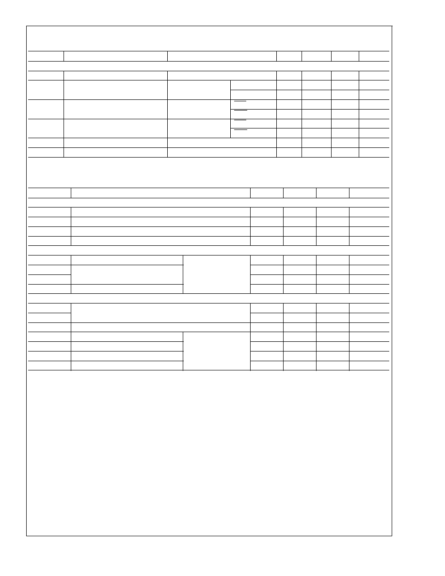
Electrical Characteristics
(Note 2)
Over Supply Voltage and Operating Temperature ranges, unless otherwise specified
Symbol
Parameter
Conditions
Min
Typ
Max
Units
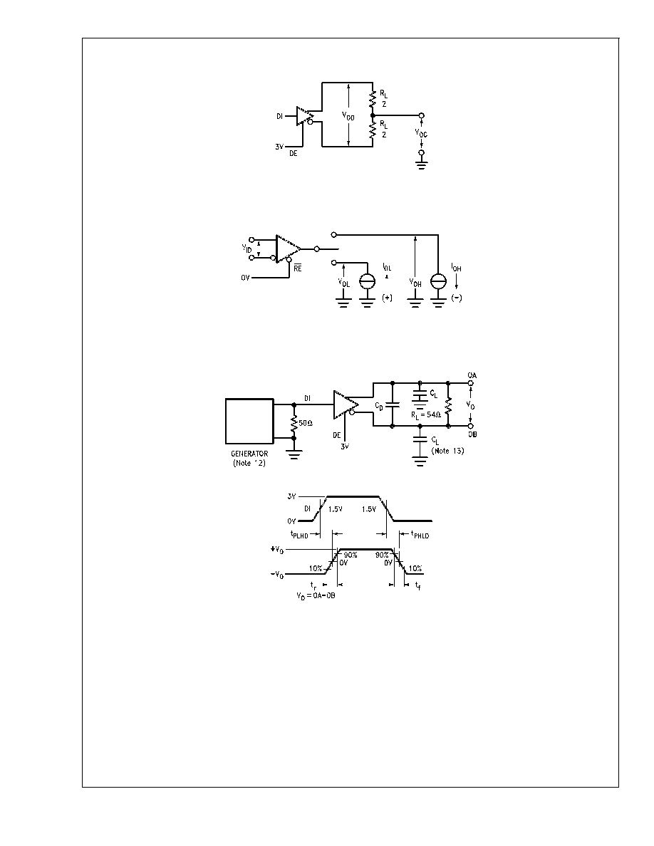
DRIVER CHARACTERISTICS
V
ODL
Differential Driver Output
I
L
= 60 mA
1.5
1.9
V
Voltage (Full Load)
V
CM
= 0V
V
OD
Differential Driver Output
R
L
= 100
(EIA-422)
2.0
3.5
V
Voltage (Termination Load)
R
L
= 54
(EIA-485)
1.5
3.2
V
IV
OD
I
Change in Magnitude of Driver
R
L
= 54
or 100
Differential Output Voltage for
(Note 4) (Figure 1)
0.2
V
Complementary Output States
(EIA-485)
V
OC
Driver Common Mode Output
R
L
= 54
3.0
V
Voltage (Note 5)
(Figure 1) (EIA-485)
IV
OC
I
Change in Magnitude of Common
(Note 4) (Figure 1)
0.2
V
Mode Output Voltage
(EIA-485)
V
OH
Output Voltage HIGH
I
OH
= -55 mA
2.7
3.2
V
V
OL
Output Voltage LOW
I
OL
= 55 mA
1.4
1.7
V
V
IH
Input Voltage HIGH
2.0
V
V
IL
Input Voltage LOW
0.8
V
V
CL
Input Clamp Voltage
I = -18 mA
-1.5
V
I
IH
Input High Current
V
I
= 2.4V (Note 3)
20
µA
I
IL
Input Low Current
V
I
= 0.4V (Note 3)
-20
µA
I
OSC
Driver Short-Circuit
V
O
= -7V
(EIA-485)
-130
-250
mA
Output Current
V
O
= 0V
(EIA-422)
-90
-150
mA
(Note 9)
V
O
= +12V
(EIA-485)
130
250
mA
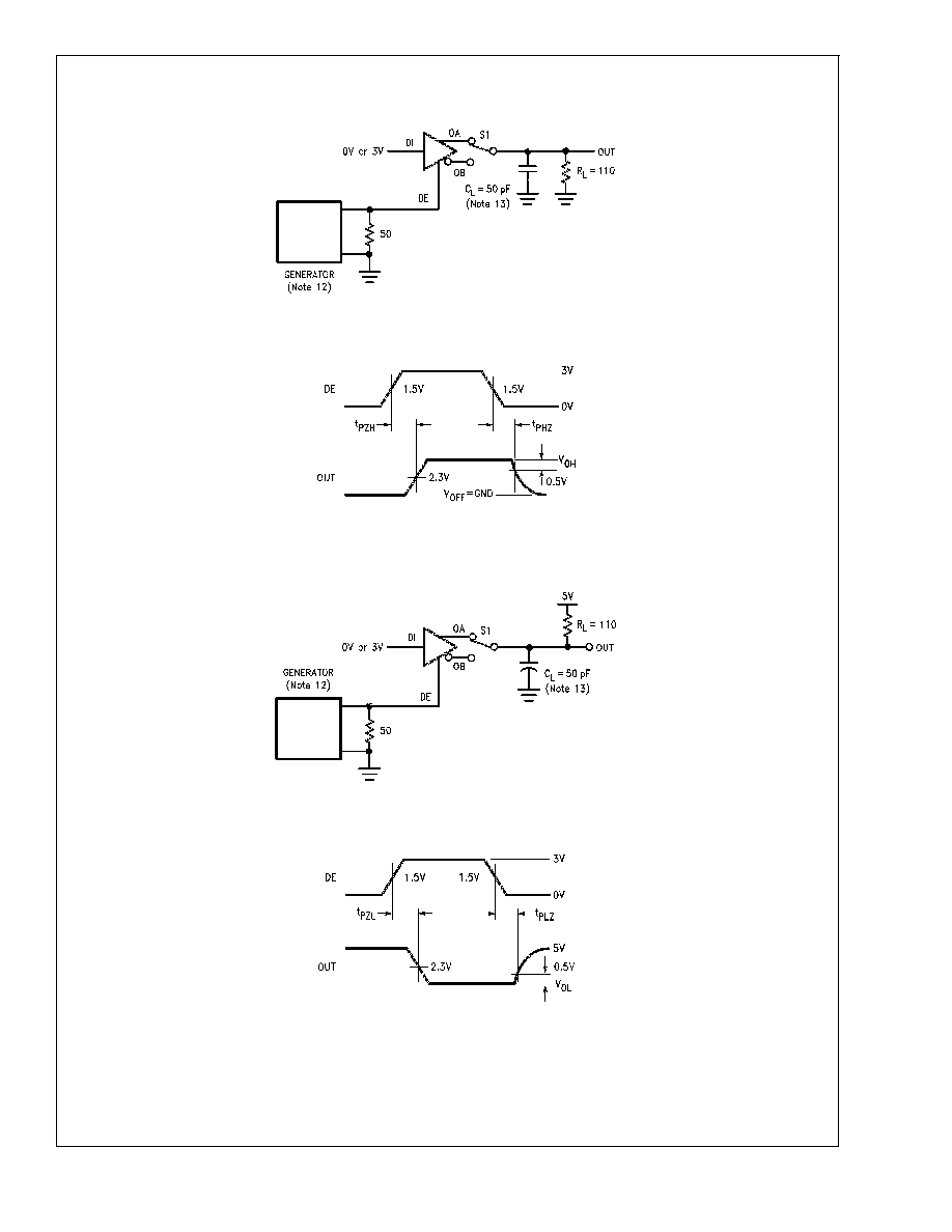
RECEIVER CHARACTERISTICS
I
OSR
Short Circuit Output Current
V
O
= 0V (Note 9)
-15
-28
-75
mA
I
OZ
TRI-STATE
®
Output Current
V
O
= 0.4V to 2.4V
20
µA
V
OH
Output Voltage High
V
ID
= 0.20V, I
OH
= -0.4 mA
2.4
3.0
V
V
OL
Output Voltage Low
V
ID
= -0.20V, I
OL
= 4 mA
0.35
0.5
V
V
TH
Differential Input High
V
O
= V
OH
, I
O
= -0.4 mA
0.03
0.20
V
Threshold Voltage
(EIA-422/485)
V
TL
Differential Input Low
V
O
= V
OL
, I
O
= 4.0 mA
-0.20
-0.03
V
Threshold Voltage (Note 6)
(EIA-422/485)
V
HST
Hysteresis (Note 7)
V
CM
= 0V
35
60
mV
DRIVER AND RECEIVER CHARACTERISTICS
V
IH
Enable Input Voltage High
2.0
V
V
IL
Enable Input Voltage Low
0.8
V
DS36950
www.national.com
2
Electrical Characteristics
(Note 2) (Continued)
Over Supply Voltage and Operating Temperature ranges, unless otherwise specified
Symbol
Parameter
Conditions
Min
Typ
Max
Units
DRIVER AND RECEIVER CHARACTERISTICS
V
CL
Enable Input Clamp Voltage
I = -18 mA
-1.5
V
I
IN
Line Input Current
Other Input = 0V
V
I
= +12V
0.5
1
mA
(Note 8)
V
I
= -7V
-0.45
-0.8
mA
I
IH
Enable Input Current High
V
OH
= 2.4V
RE4 or DE
20
µA
REC
60
µA
I
IL
Enable Input Current Low
V
OL
= 0.4V
RE4 or DE
-20
µA
REC
-60
µA
I
CC
Supply Current (Note 10)
No Load, Outputs Enabled
75
90
mA
I
CCZ
Supply Current (Note 10)
No Load, Outputs Disabled
50
70
mA
Switching Characteristics
Over Supply Voltage and Operating Temperature ranges, unless otherwise specified
Symbol
Conditions
Min
Typ
Max
Units
DRIVER SINGLE-ENDED CHARACTERISTICS
t
PZH
R
L
= 110
(Figure 4)
35
40
ns
t
PZL
R
L
= 110
(Figure 5)
25
40
ns
t
PHZ
R
L
= 110
(Figure 4)
15
25
ns
t
PLZ
R
L
= 110
(Figure 5)
35
40
ns
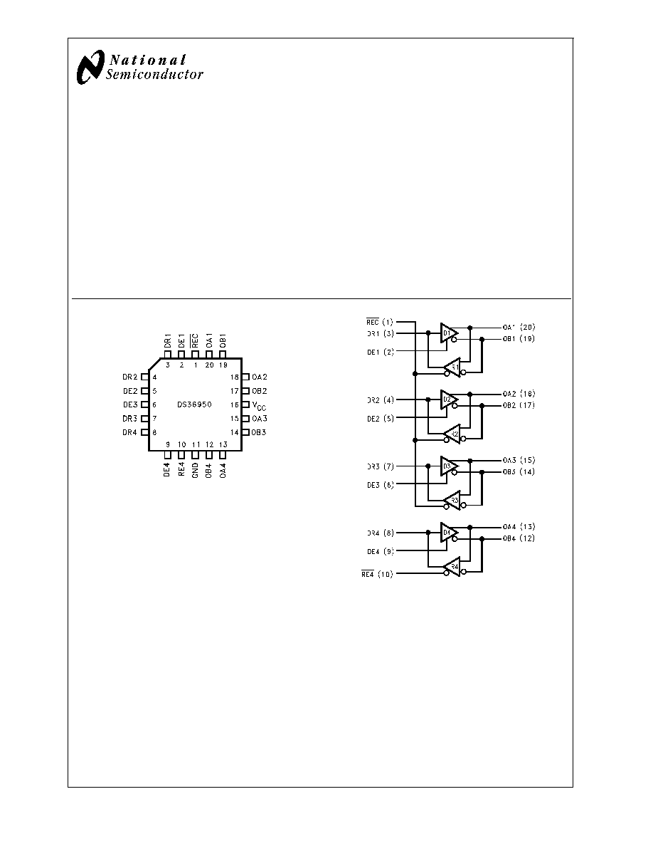
DRIVER DIFFERENTIAL CHARACTERISTICS
t
R
, t
F
Rise & Fall Time
R
L
= 54
13
16
ns
t
PLHD
Differential Propagation
C
L
= 50 pF
9
15
19
ns
t
PHLD
Delays (Note 15)
C
D
= 15 pF
9
15
19
ns
t
SKD
|t
PLHD
- t
PHLD
| Differential Skew
(Figures 3, 8)
3
6
ns
RECEIVER CHARACTERISTICS
t
PLHD
Differential Propagation Delays
9
14
19
ns
t
PHLD
C
L
= 15 pF, V
CM
= 1.5V (Figure 6)
9
14
19
ns
t
SKD
|t
PLHD
- t
PHLD
| Differential Receiver Skew
1
3
ns
t
ZH
Output Enable Time to High Level
15
22
ns
t
ZL
Output Enable Time to Low Level
C
L
= 15 pF
20
30
ns
t
HZ
Output Disable Time from High Level
(Figure 7)
10
17
ns
t
LZ
Output Disable Time from Low Level
17
25
ns
Note 1: "Absolute Maximum Ratings" are those values beyond which the safety of the device cannot be guaranteed. They are not meant to imply that the devices
should be operated at these limits. The tables of "Electrical Characteristics" specify conditions for device operation.
Note 2: Current into device pins is define as positive. Current out of device pins is defined as negative. All voltages are referenced to ground unless otherwise
specified.
Note 3: I
IH
and I
IL
includes driver input current and receiver TRI-STATE leakage current.
Note 4:
IV
OD
I and
IV
OC
I are changes in magnitude of V
OD
and V
OC
, respectively, that occur when the input changes state.
Note 5: In EIA Standards EIA-422 and EIA-485, V
OC
, which is the average of the two output voltages with respect to ground, is called output offset voltage, V
OS
.
Note 6: Threshold parameter limits specified as an algebraic value rather than by magnitude.
Note 7: Hysteresis defined as V
HST
= V
TH
- V
TL
.
Note 8: I
IN
includes the receiver input current and driver TRI-STATE leakage current.
Note 9: Short one output at a time.
Note 10: Total package supply current.
Note 11: All typicals are given for V
CC
= 5.0V and T
A
= 25°C.
DS36950
www.national.com
3