
© 2000 National Semiconductor Corporation
http://www.national.com
Printed in the U.S.A.
N
Section I. Introduction
The CLC3790093 Data Capture Board enables simple evaluation
of National Semiconductor's High Speed Analog to Digital Con-
verters (ADCs) and the Diversity Receiver Chip Set (DRCS). The
Data Capture Board interfaces the outputs of these devices to the
standard serial port available on the back of most Personal
Computers (PCs). We have provided PC software to control the
data capture function and Matlab
Æ
scripts for data analysis.
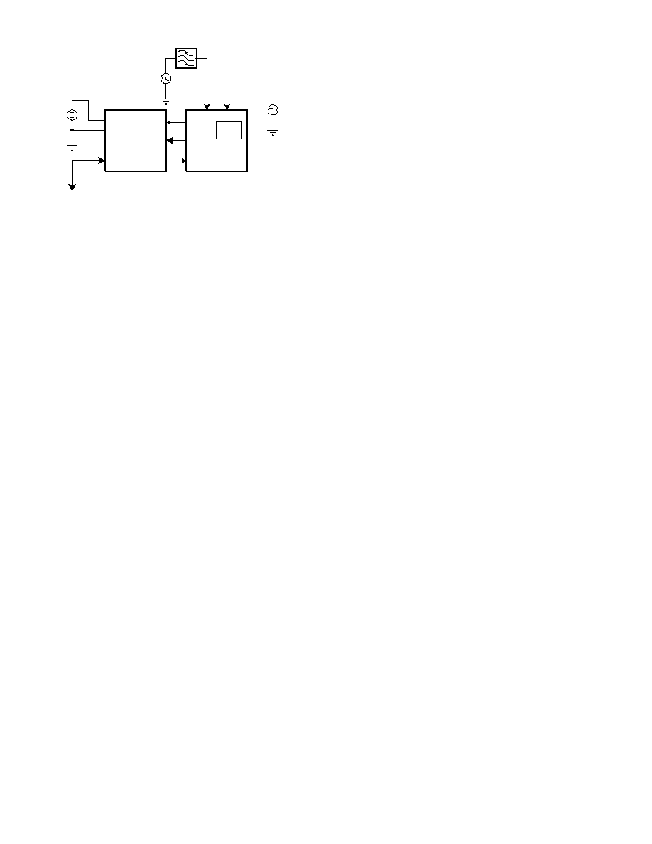
A block diagram of the evaluation test bed is shown below.
The Data Capture Board contains a field-programmable gate
array (FPGA) that controls its operation. An EPROM configures
the FPGA after power is applied. The serial interface is provided
by a UART (Universal Asynchronous Receiver/Transmitter), an
oscillator, and a level translator IC. The captured data is stored in
either three 32K x 8 static RAMs (organized into 24-bit words) or
in a FIFO containing 32K 18-bit words. LEDs provide a visual
indication of activity. DIP switches and a jumper configure several
capture functions.
Section II. Capturing Data from ADC
Evaluation Boards
Getting Started
To use the Data Capture board to capture data from a National
Semiconductor Analog to Digital converter, you will need the
following hardware, software, and documentation.
CLC-CAPT-PCASM
Data Capture Board User's Guide
Table of Contents
I. Introduction
II. Capturing Data from ADC
Evaluation
Boards
III. Capturing Data from the DRCS
Evaluation Boards
IV. Data Analysis using Matlab
Script
Files
October 2000
CLC-CAPT
-PCASM
Data Capture Boar
d User'
s Guide
CLCXXXX
A/D Converter
Evaluation Board
Digital Receiver
Evaluation Board
Data
Capture
Board
National Semiconductor
High-Speed Converter
Evaluation Test Bed
http://www.national.com
2
Hardware
1. CLC3790093 Data Capture Board
(CLC-CAPT-PCASM)
2. CLCXXXX Evaluation Board. Several ADC products
can be evaluated with this system. Each product
has a unique evaluation board which plugs into the
data capture board. In order to determine the
compatibility of specific ADC evaluation boards to the
data capture board, please refer to the "Basestation
A/D Converter Evaluation Board Interoperability Guide"
available on our website at http://www.national.com/
appinfo/wbp.
3. Personal Computer. An IBM-Compatible PC running
Windows
Æ
95, Windows
Æ
98, or Windows
Æ
NT. The
PC should have an available serial port capable of
operating at 115,200 baud. These ports are usually
labeled and referred to as COM1 and COM2. The
captured data is stored in a file on the PC to allow
custom analysis.
4. Serial Cable. A standard serial interface cable is
provided. This cable connects the data capture
board to the PC.
5. Power Supply. The data capture board requires a
single +5V supply. This power is applied at
connector J3. A 2-amp supply will provide enough
current for the evaluation board and the data
capture
board. Note that the power for the
evaluation board is provided from the data capture
board through the 64-pin connector J1.
6. Input signal. You can provide any type of input
signal that you feel is appropriate to your system
testing. The data analysis software provided with the
data capture board is oriented toward analysis of
single tone sinewave inputs. Our recommendation
for high purity, low phase noise reference signal
sources is the Hewlett Packard HP8644B
synthesizer. It provides an excellent input stimulus
for evaluating ADC performance.
7. Bandpass or lowpass filter. Even with a good
sinewave source, you will need to filter out the
harmonics of the signal source. A bandpass filter
also enables filtering of the wideband noise of the
reference source. As an example, Allen Avionics
(Mineola, NY) passive filters are used for most of
our converter testing.
8. Clock Source. If you wish to test the ADC with a fixed
clock frequency, you may install a standard TTL
oscillator in the socket provided on the evaluation
board. Otherwise, you will need to provide a low
phase noise sinewave or square wave clock source
at the appropriate SMA connector on the evaluation
board. An amplitude of 10 to 16dBm is recommended.
Here, again, the HP 8644B is a good choice.
Software
1.
National Semiconductor Software. All of the
required software is provided on a CD-ROM. To
install the software now, insert the CD-ROM into
your computer and follow the directions. The default
installation copies all of the files to a directory called
"c:\nsc". The data capture software is called
"capture.exe".
2. Matlab. A copy of Matlab version 5.1 or later is
required to operate the analysis routines. If you
simply
wish to capture data to a file on your
PC and process the data with your own analysis
software, then you will not need Matlab. For more
information about Matlab, please see their website
at
http://www.mathworks.com
.
3. Matlab script files. The Matlab script files for data
analysis are located in the "c:\nsc\mfiles" directory.
These script files are run from the Matlab command
prompt.
Documentation
Applicable product data sheets and user guides can be found
on the provided CD-ROM, with the most current versions
available on our website at:
http://www.national.com/appinfo/wbp
If you are evaluating the Diversity Receiver Chip Set,
please refer to Section III of this manual.
Operation of Data Capture Board
When evaluating the performance of an ADC, the data
capture board has two main modes of operation. In the
first mode, data is captured from the evaluation board
under test at the full sample rate of the ADC. A
contiguous set of 32k data samples is captured into a
FIFO memory on the board, and then this data is moved
over to the PC at a slower rate. The data set is stored in a
file on the hard drive for later analysis. The data is stored
in an ASCII file in exactly the format that it is output from
the converter. For the CLC5957, the two's complement
12-Bit data is stored as numbers ranging from 0 to 4095.
In the case of the 14-bit CLC5958, the two's complement
data ranges from 0 to 16383. Each value is terminated
with a carriage return, hexadecimal 0D. Note that the
two's complement number can be converted to offset
binary by inverting the MSB. This is the first step in the
Matlab routine for FFT analysis.
BPF
Ain
CLK
VCC
GND
OPTIONAL
CLOCK SOURCE
FILTERED
SIGNAL
SOURCE
+5V
VCC
(2A)
Data
10-16dBm
To PC Serial
COMM PORT #1 or #2
64P I/O
CONNECTOR
Clock
Power
Optional
TTL
Oscillator
ADC
Evaluation
Board
Data
Capture
Board
Serial I/O

3
http://www.national.com
Histogram Mode
In the second mode of operation, the "Histogram" mode,
the data capture board operates as a hardware histo-
grammer. The board does not collect a contiguous record
from the ADC; instead, it compiles statistical information
by counting the number of times that the ADC
outputs each code. The most significant 15 bits of the
converter define 32K histogram bins. The MSB of the
data is inverted before being stored (all data is treated as
offset binary format). ADC data is aligned to the least
significant bit, and unused higher bits are set to 0s. Each
bin is cleared initially. The ADC output code is used as
the address for the SRAM on the board, and as each
code is read by the Data Capture board, the data at that
location in the SRAM is read, incremented and written
back to the SRAM. This counting requires multiple clock
cycles, so the data is not counted in real time. In fact, 11
samples of data are missed for each sample that is
counted. The histogram capture terminates when a bin
reaches the count specified by DIP switches 4 and 5. The
32K histogram bin counts are then returned via the serial
port. If the input signal to the ADC is a pure
sinusoid,
then the histogram information can be
compared to the theoretical probability density of a
sinusoid and the linearity of the ADC can be calculated.
The supplied Matlab script DNL_INL uses this method.
Please refer to the IEEE Standard for Digitizing Waveform
Recorders (IEEE Std 1057-1994) for more information
about this technique.
Hardware Configuration
Jumpers
The data capture board has 2 jumpers that must be
configured before use. The first jumper, WCLK, selects
the clock source for the FIFO. When capturing data from
an ADC evaluation board,
WCLK should be set to
RDY2
. This selects the DR (Data Ready) clock line from
the ADC evaluation board pin 20B. The second jumper,
VCCD, sets the supply voltage for the ADC output buff-
ers. Unless the ADC evaluation board instructions specify
otherwise, this jumper should be set to +5.
Data Capture Board Block Diagram
DIP Switches
Five of the eight DIP switches are used to configure
several capture functions as follows.
DIP switch 1:
This DIP switch specifies whether a
Diversity Receiver Evaluation Board or an
ADC Evaluation Board is attached to the Data
Capture Board.
ON
ADC Evaluation Board is attached.
Captured data is aligned to the least significant
bit with unused higher bits set to 0s.
DIP switches 2 and 3:
When DIP switch 1 is ON to
indicate that an ADC Evaluation Board is attached,
DIP switches 2 and 3 specify the width of the ADC
data so it can be aligned to the least significant bit
and unused higher bits can be set to 0s.
DIP switches 4 and 5:
These DIP switches specify the
maximum histogram bin count. The histogram
capture terminates when any bin reaches the count
specified by these switches.
A maximum count of 16384 corresponds to approxi-
mately 2.5 million total samples for a 12-Bit ADC. The
capture is very fast (on the order of 1 second for a 52
MSPS clock rate) so there is not much advantage in set-
ting the switches for a lower maximum count. The other
settings are more useful for the DRCS evaluations
because the effective clock rate can become very low
with certain output formats and decimation ratios.
CLC5956 Data
Analog Input
Condition
Offset Binary Number
Two's Complement
ASCII Value Stored
Ain- >> Ain
- Full Scale
0000 0000 0000
1000 0000 0000
2048
Ain- > Ain
- Mid Scale
0111 1111 1111
1111 1111 1111
4095
Ain > Ain-
+ Mid Scale
1000 0000 0000
0000 0000 0000
0
Ain >> Ain-
+ Full Scale
1111 1111 1111
1111 1111 1111
2047
CLC5958 Data
Analog Input
Condition
Offset Binary Number
Two's Complement
ASCII Value Stored
Ain- >> Ain
- Full Scale
00 0000 0000 0000
10 0000 0000 0000
8192
Ain- > Ain
- Mid Scale
01 0111 1111 1111
11 1111 1111 1111
16383
Ain > Ain-
+ Mid Scale
10 0000 0000 0000
00 0000 0000 0000
0
Ain >> Ain-
+ Full Scale
11 1111 1111 1111
01 1111 1111 1111
8191
FPGA Performs:
State Machine
Signal Format Conversion
Data Routing
Data
12-18
Bits
J1
Eurocard
Connector
FPGA
SRAM
24-bits
32k depth
FIFO
18-bits
32k depth
UART
J9
9-pin
Serial Cable
Connector
24
Serialized
Data Stream
Note: Primary data path shown.
Control lines not shown
RDY2
WCLK
Clock
Switch:
2
3
Number of Bits in ADC
OFF
OFF
18
OFF
ON
16
ON
OFF
14
ON
ON
12
Switch:
4
5
Maximum Count
OFF
OFF
16384
OFF
ON
8192
ON
OFF
4096
ON
ON
2048

http://www.national.com
4
SMA Connectors
The output clock SMA connector provides a signal that
can be used to phase lock a signal source. The
frequency is that of the input clock signal divided by 2.
For example, with an attached CLC5958 ADC evaluation
board at 52MSPS the clock output signal will be a
26MHz square wave. The second SMA connector is
currently unused.
Serial Port
The serial port is configured at 115,200 baud with one
stop bit, no parity, and 8-bits per character. Although the
DSR, CTS, and RTS control signals are connected, they
are not used. XON/XOFF flow control is supported. The
flow of returned data pauses after an XOFF character
(DC3, ctrl-S, hexadecimal 13) has been received. The
flow of returned data resumes after an XON character
(DC1, ctrl-Q, hexadecimal 11) has been received. The
Data Capture Board initializes as if an XON character
had been received.
Power Up the System
Once the WCLK jumper, VCCD jumper, and the DIP
switches have been set, (for example, for the CLC5957
we have set WCLK at RDY2, VCCD at +5, and DIP
switches 1,2,3,4,5 as ON,ON,ON,OFF,OFF) connect the
evaluation board to the data capture board, apply power,
clock, and signal to the boards, and connect the serial
cable to the PC. Some PCs will need to be rebooted at
this point, but it may not be necessary with your PC.
In the software configuration section, next, we will
check
the
communication between the PC and the data
capture board.
Light Emitting Diode (LED) Status Monitors
3 of the 6 LEDs are used to provide status indications.
LED 1:
This LED is connected to an address line of the
static RAM ICs. While the static RAM is being
written or read, it blinks. After the Data Capture
Board is powered up and the FPGA is initialized, it is
on to indicate that the board is ready. After all the
SRAM data has been output, it is off.
LED 2:
This LED is on when captured data is available
to be output to the serial port. After all the data has
been output, it is off.
LED 6:
This LED is connected to the clock signal
selected by DIP switch 1. When the clock is
toggling, it will be on at less than full intensity.
So, at this point in your setup, you should have LED 1 on
at full intensity and LED 6 on at reduced intensity. You are
now ready to configure the software for data capture.
Software Configuration
Run the program
"capture.exe"
. It is located in the direc-
tory that you chose during the CD-ROM installation. The
default directory is
"c:\nsc\"
. You can also use the start
menu: start
programs
nsc
capture.
When you run
capture.exe
, you will see the following
window pop up onto your PC:
This is the data capture control panel. It is small to
conserve monitor area for other programs. The main
function of the panel is to initiate data capture. Before we
capture data we must configure the computer and the
board. By clicking on the
control panel
with the RIGHT
mouse button (right click), we bring up the following
configuration menu:
The first thing to configure is the COM port on the
computer, so move the mouse to
"Configure I/O"
and
click with the LEFT mouse button. This will bring up the
following menu:
Select the COM port that you have attached to the data
capture board, and press
"OK"
. The computer will then
send a command to the data capture board. If the data
capture board responds and the COM port interface is
operating correctly, the
"Configure I/O"
menu will disap-
pear, and the Data Capture control panel will return. If
there is a problem with the COM port interface, you will
get the following message:
5
http://www.national.com
Verify the connections and, if necessary, try the other
COM port. (Note that you must have a clock applied to
the ADC Evaluation board during this communication
verification stage. Check to make sure that either an
external clock or the TTL oscillator is installed, and that
LED6 is on at reduced intensity.) Once you get a proper
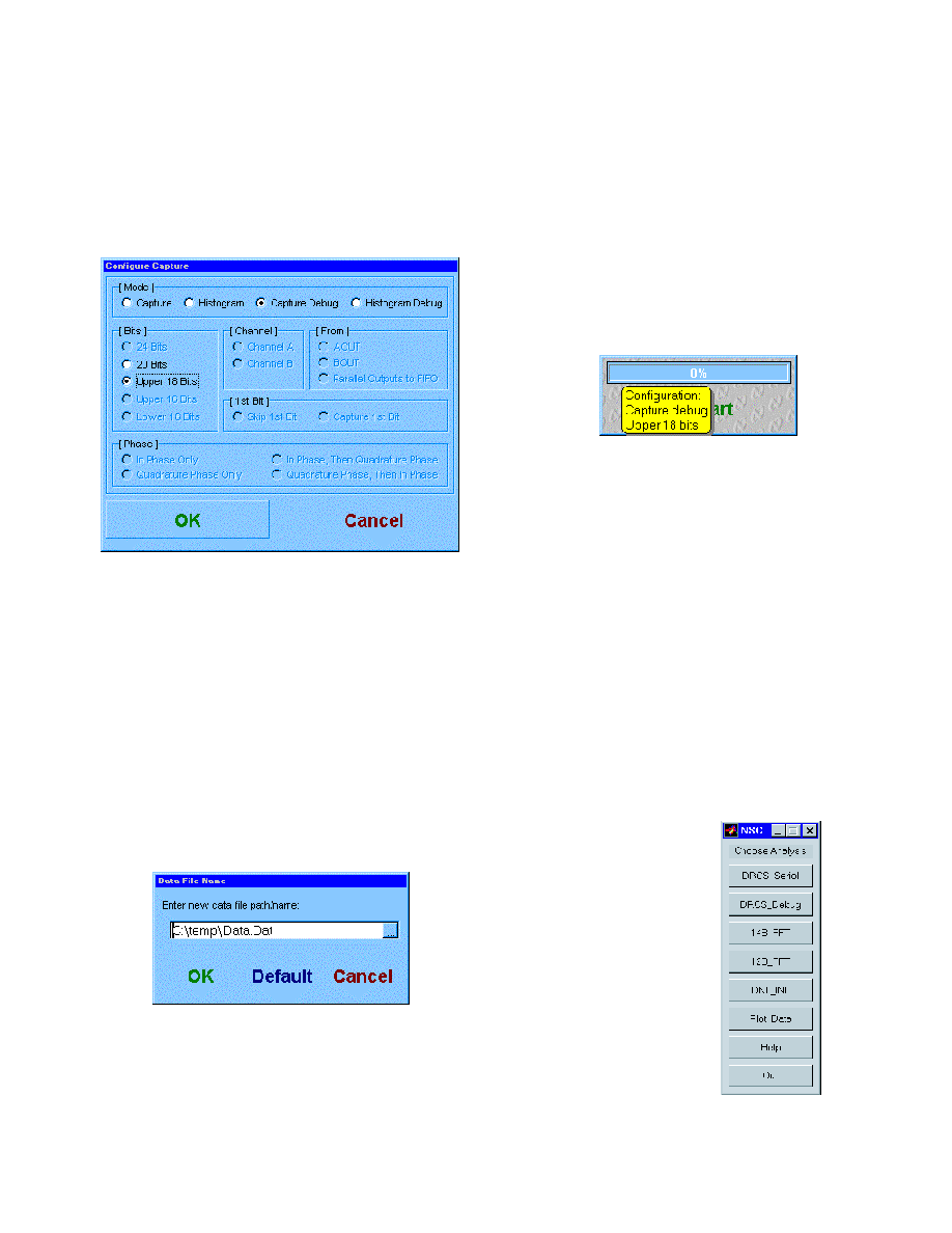
exit from this step, you are ready to configure the capture
board. Right click on the capture control panel, then left
click on
"Configure Capture."
You will see the following
screen:
To configure the capture board for direct capture of a
contiguous 32k point record of ADC output codes, click
on the selections shown above. Left click on
"Capture
Debug"
and select
"Upper 18 Bits."
The names of these
selections may seem rather cryptic when you are simply
capturing ADC data. The label names are derived from
functions in the DRCS and CLC5902, so they might
seem out of context for ADC capture uses. Don't worry
about the label names, just make sure you have selected
the modes as shown above. Then click on
"OK."
One final configuration remains. You need to tell the
program where to store your data. Right click on the
capture control panel, then left click on
"Change Data
File."
You will see the following menu:
By left clicking on the little box to the right of the text entry
window, you can select any disk, directory, and file name
that suits you. However, we recommend that you start
with the default file name and location shown. Click on
"Default"
and then on
"OK"
. If you do not have a
C:\temp directory, please make one. The reason for this
is that the Matlab script files for data analysis look
automatically for the file
C:\temp\data.dat
. If you wish to
store the data elsewhere, you will need to modify the
Matlab m-files to look for your data file in a different
location. Obviously, if you are using your own software
for data analysis this is not a concern.
Capture Data!
We are finally ready to capture data from the ADC. As a
final check, you can move the mouse until it is on top of
the progress bar (the big bar on the data capture control
panel that now reads (0%). You should see a little yellow
box appear that confirms your capture settings.
Now, simply left-click on the
"Start"
button on the capture
control panel to start the process. You will see LED 2 light
up on the board, and the bar at the top of the capture
control panel will show the progress of the data transfer.
At 52MSPS, the 32768 samples are collected in only 630
microseconds; the rest of the time is the serial port trans-
fer. Typical times for this transfer are on the order of 10 to
15 seconds. To analyze the data using the Matlab Mfiles
that we have provided, please start Matlab at this time. To
include the provided script files in your Matlab path, type
the following command at the Matlab command prompt:
>> path(path,'c:\nsc\mfiles')
Alternatively, you can change directories at the Matlab
prompt until this is the current directory. From the Matlab
command prompt, type
"analysis_menu"
. This will bring
up the following menu: