Document Outline
- COVER
- FEATURES
- ORDERING INFORMATION
- BLOCK DIAGRAM
- COMPARISON WITH THE uPD720100A
- PIN CONFIGURATION
- 1. PIN INFORMATION
- 2. HOW TO CONNECT TO EXTERNAL ELEMENTS
- 2.1 Handling Unused Pins
- 2.2 USB Port Connection
- 2.3 PLL Capacitor Connection
- 2.4 X'tal Connection
- 2.5 External Serial ROM Connection
- 3. ELECTRICAL SPECIFICATIONS
- 3.1 Buffer List
- 3.2 Terminology
- 3.3 Electrical Specifications
- 3.4 Timing Diagram
- 4. PACKAGE DRAWINGS
- 5. RECOMMENDED SOLDERING CONDITIONS

The information in this document is subject to change without notice. Before using this document, please
confirm that this is the latest version.
Not all products and/or types are available in every country. Please check with an NEC Electronics
sales representative for availability and additional information.
MOS INTEGRATED CIRCUIT
µ
PD720101
USB2.0 HOST CONTROLLER
Document No. S16265EJ4V0DS00 (4th edition)
Date Published June 2004 NS CP (N)
Printed in Japan
DATA SHEET
The mark shows major revised points.
2002
The
µ
PD720101 complies with the Universal Serial Bus Specification Revision 2.0 and Open Host Controller
Interface Specification for full-/low-speed signaling and Intel's Enhanced Host Controller Interface Specification for
high-speed signaling and works up to 480 Mbps. The
µ
PD720101 is integrated 3 host controller cores with PCI
interface and USB2.0 transceivers into a single chip.
Detailed function descriptions are provided in the following user's manual. Be sure to read the manual before designing.
µ
PD720101 User's Manual: S16336E
FEATURES
∑ Compliant with Universal Serial Bus Specification Revision 2.0 (Data rate 1.5/12/480 Mbps)
∑ Compliant with Open Host Controller Interface Specification for USB Rev 1.0a
∑ Compliant with Enhanced Host Controller Interface Specification for USB Rev 1.0
∑ PCI multi-function device consists of two OHCI host controller cores for full-/low-speed signaling and one EHCI host
controller core for high-speed signaling.
∑ Root hub with 5 (max.) downstream facing ports which are shared by OHCI and EHCI host controller cores.
∑ All downstream facing ports can handle high-speed (480 Mbps), full-speed (12 Mbps), and low-speed (1.5 Mbps)
transaction.
∑ Configurable number of downstream facing ports (2 to 5)
∑ 32-bit 33 MHz host interface compliant to PCI Specification release 2.2
∑ Supports PCI Mobile Design Guide Revision 1.1
∑ Supports PCI-Bus Power Management Interface Specification release 1.1
∑ PCI bus bus-master access
∑ System clock is generated by 30 MHz X'tal or 48 MHz clock input.
- System clock frequency should be set from system software (BIOS) or EEPROM. More detail, see
µ
PD720101
User's Manual.
∑ Operational registers direct-mapped to PCI memory space
∑ Legacy support for all downstream facing ports. Legacy support features allow easy migration for motherboard
implementation.
∑ 3.3 V power supply, PCI signal pins have 5 V tolerant circuit.
ORDERING INFORMATION
Part Number
Package
µ
PD720101GJ-UEN 144-pin
plastic
LQFP (Fine pitch) (20
◊ 20)
µ
PD720101F1-EA8
144-pin plastic FBGA (12
◊ 12)

Data Sheet S16265EJ4V0DS
2
µ
PD720101
BLOCK DIAGRAM
INTB0
PCI Bus
PCI Bus Interface
Arbiter
OHCI
Host
Controller
#1
OHCI
Host
Controller
#2
EHCI
Host
Controller
Root Hub
PHY
USB Bus
Port 1
Port 2
Port 3
Port 4
Port 5
PME0
WakeUp_Event
WakeUp_Event
WakeUp_Event
INTA0
INTC0
SMI0
Remark INTB0/INTC0 can be shared with INTA0 through BIOS setting. (Planning)

Data Sheet S16265EJ4V0DS
3
µ
PD720101
PCI Bus Interface
: handles 32-bit 33 MHz PCI bus master and target function which comply with PCI
specification release 2.2. The number of enabled ports is set by bit in configuration
space.
Arbiter
: arbitrates among two OHCI host controller cores and one EHCI host controller core.
OHCI Host Controller #1
: handles full- (12 Mbps)/low-speed (1.5 Mbps) signaling at port 1, 3, and 5.
OHCI Host Controller #2
: handles full- (12 Mbps)/low-speed (1.5 Mbps) signaling at port 2 and 4.
EHCI Host Controller
: handles high- (480 Mbps) signaling at port 1, 2, 3, 4, and 5.
Root Hub
: handles USB hub function in host controller and controls connection (routing) between
host controller core and port.
PHY
: consists of high-speed transceiver, full-/low-speed transceiver, serializer, deserializer,
etc.
INTA0
: is the PCI interrupt signal for OHCI Host Controller #1.
INTB0
: is the PCI interrupt signal for OHCI Host Controller #2.
INTC0
: is the PCI interrupt signal for EHCI Host Controller.
SMI0
: is the interrupt signal which is specified by Open Host Controller Interface Specification
for USB Rev 1.0a and Enhanced Host Controller Interface Specification Rev 1.0. The
SMI signal of each OHCI Host Controller and EHCI Host Controller appears at this
signal.
PME0
: is the interrupt signal which is specified by PCI-Bus Power Management Interface
Specification release 1.1. Wakeup signal of each host controller core appears at this
signal.
COMPARISON WITH THE
µPD720100A
µ
PD720100A
µ
PD720101 (2nd generation)
EHCI revision
0.95
1.0
EHCI 1
1
OHCI 2
2
Legacy support
Parallel IRQ out support
No parallel IRQ support
Clock
48 MHz OSC or 30 MHz OSC/X'tal
48 MHz OSC or 30 MHz X'tal
Package
176-pin BGA (FP) or 160-pin LQFP
144-pin BGA (FP) or 144-pin LQFP

Data Sheet S16265EJ4V0DS
4
µ
PD720101
PIN CONFIGURATION
∑ 144-pin plastic LQFP (Fine pitch) (20 ◊ 20)
µ
PD720101GJ-UEN
Top View
V
DD
V
DD
NTEST1
NANDTEST
TEST
XT1/SCLK
XT2
LEGC
VCCRST0
SMI0
PME0
PCLK
VBBRST0
V
DD
V
SS
V
DD_PCI
INTA0
INTB0
INTC0
GNT0
REQ0
AD31
AD30
V
SS
AD29
AD28
AD27
AD26
AD25
AD24
CBE30
IDSEL
V
DD
V
SS
V
SS
V
SS
RSDM1
DM1
V
DD
DP1
RSDP1
V
SS
RSDM2
DM2
V
DD
DP2
RSDP2
V
SS
V
DD
V
SS
RSDM3
DM3
V
DD
DP3
RSDP3
V
SS
RSDM4
DM4
V
DD
DP4
RSDP4
V
SS
V
SS
V
SS
V
SS
V
SS
AD7
CBE00
AD8
AD9
AD10
AD11
AD12
V
DD
AD13
AD14
AD15
V
SS
CBE10
PAR
SERR0
PERR0
STOP0
V
DD_PCI
DEVSEL0
TRDY0
IRDY0
FRAME0
CBE20
AD16
AD17
AD18
V
DD
AD19
AD20
AD21
AD22
SMC
AD23
V
SS
V
SS
V
DD
AV
DD
AV
DD
RREF
N.C.
N.C.
AV
SS
AV
SS
AV
SS
(R)
RSDP5
DP5
V
DD
DM5
RSDM5
V
SS
PPON5
TEB
PPON4
PPON3
PPON2
V
SS
V
DD
OCI3
AMC
OCI4
OCI2
OCI5
PPON1
OCI1
SRMOD
SRCLK
SRDTA
V
DD_PCI
CRUN0
AD0
AD1
AD2
AD3
AD4
AD5
AD6
V
DD
V
DD
1
5
10
15
20
25
35
30
40
50
55
45
60
65
70
85
90
75
80
95
100
105
110
115
130
135
144
120
125
140

Data Sheet S16265EJ4V0DS
5
µ
PD720101
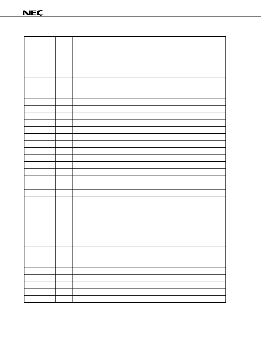
Pin No.
Pin Name
Pin No.
Pin Name
Pin No.
Pin Name
Pin No.
Pin Name
1 V
DD
37
V
SS
73
V
DD
109
V
SS
2 V
DD
38
V
SS
74
V
DD
110
V
SS
3 OCI1
39 AD23
75 AD6
111
RSDM1
4 PPON1 40 AD22
76 AD5
112
DM1
5 OCI2
41 AD21
77 AD4
113
V
DD
6 PPON2 42 AD20
78 AD3
114
DP1
7 OCI3
43 V
DD
79
AD2 115
RSDP1
8 PPON3 44 AD19
80 V
DD_PCI
116
V
SS
9 OCI4
45 AD18
81 AD1
117
RSDM2
10 PPON4
46 AD17
82 AD0
118 DM2
11 OCI5
47 AD16
83 CRUN0
119 V
DD
12 PPON5
48 CBE20
84 N.C.
120 DP2
13 VCCRST0 49 FRAME0 85 N.C.
121 RSDP2
14 PME0
50 IRDY0
86 SMI0
122 V
SS
15 PCLK
51 TRDY0
87 AMC
123 V
SS
16 VBBRST0 52 DEVSEL0 88 TEB
124 V
DD
17 V
DD_PCI
53
STOP0 89
SMC 125
V
SS
18 V
SS
54
V
SS
90
LEGC
126
RSDM3
19 V
DD
55
V
DD
91
TEST
127
DM3
20 INTA0
56 V
DD_PCI
92
NTEST1
128
V
DD
21 INTB0
57 PERR0
93 V
DD
129
DP3
22 INTC0
58 SERR0
94 XT2
130 RSDP3
23 GNT0
59 PAR
95 XT1/SCLK 131 V
SS
24 REQ0
60 CBE10
96 SRCLK
132 RSDM4
25 AD31
61 AD15
97 SRMOD
133 DM4
26 AD30
62 AD14
98 SRDTA
134 V
DD
27 AD29
63 AD13
99 NANDTEST 135 DP4
28 AD28
64 AD12
100 V
SS
136
RSDP4
29 AD27
65 AD11
101 V
SS
137
V
SS
30 AD26
66 AD10
102 AV
DD
138
RSDM5
31 AD25
67 AD9
103 RREF
139 DM5
32 AD24
68 AD8
104 AV
SS
(R) 140
V
DD
33 CBE30
69 CBE00
105 AV
SS
141
DP5
34 IDSEL
70 AD7
106 AV
DD
142
RSDP5
35 V
SS
71
V
SS
107
AV
SS
143
V
SS
36 V
DD
72
V
SS
108
V
DD
144
V
SS
Remark AV
SS
(R) should be used to connect RREF through 1 % precision reference resistor of 9.1 k
.
Pins 84 and 85 must be clamped high on the board.

Data Sheet S16265EJ4V0DS
6
µ
PD720101
∑ 144-pin plastic FBGA (12 ◊ 12)
µ
PD720101F1-EA8
Bottom View
25 26 27 28 29 30 31 32 33 34 35 36 14
24 71 72 73 74 75 76 77 78 79 80 81 82 37 13
23 70 111 112 113 114 115 116 117 118 119 120
83 38 12
22 69
110 137 138 139 140
121
84 39 11
21
68
109
122
85
40
10
20
67
108
136
141 123
86
41
9
19
66
107
135
142 124
87
42
8
18
65
106
134
143 125
88
43
7
17
64
105
133
144 126
89
44
6
16
63
104
127
90
45
5
15 62
103 132 131 130 129
128
91 46 4
14 61 102 101 100 99 98 97 96 95 94 93 92 47 3
13 60 59 58 57 56 55 54 53 52 51 50 49 48 2
12 11 10 9 8 7 6 5 4 3 2 1 1
P N M L K J H G F E D C B A

Data Sheet S16265EJ4V0DS
7
µ
PD720101
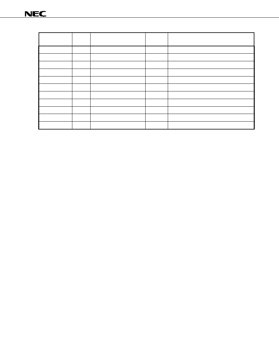
Pin No.
Pin Name
Pin No.
Pin Name
Pin No.
Pin Name
Pin No.
Pin Name
1 V
SS
37
V
DD
73
V
DD
109
NANDTEST
2 AD23
38 V
DD
74
RSDP1
110
V
SS
3 AD20
39 PPON2 75 V
DD
111
AV
SS
4 AD18
40 OCI4
76 V
DD
112
V
SS
5 CBE20
41 PPON5 77 DP3
113
DM2
6 TRDY0 42 PCLK
78 V
DD
114
RSDP2
7 SERR0 43 INTC0
79 RSDM5 115
V
SS
8 AD15
44 AD31
80 V
DD
116
V
DD
9 AD12
45 AD28
81 DP5
117
RSDM4
10 AD9
46 AD25
82 V
SS
118
DP4
11 AD7
47 V
DD
83
OCI1
119
V
SS
12 V
SS
48
V
SS
84
OCI2
120
PPON1
13 V
DD
49
V
SS
85
OCI3
121
PPON3
14 V
DD
50
AD22
86
OCI5
122
PPON4
15 AD3
51 AD21
87 VBBRST0 123 VCCRST0
16 AD1
52 V
DD
88
INTB0
124
V
DD_PCI
17 N.C.
53 AD16
89 AD30
125 INTA0
18 AMC
54 DEVSEL0 90 AD26
126 REQ0
19 XT2
55 PERR0
91 AD24
127 AD29
20 SRMOD
56 AD14
92 IDSEL
128 AD27
21 V
SS
57
AD10
93
CBE30
129
IRDY0
22 RREF
58 AD8
94 AD19
130 V
SS
23 V
DD
59
CBE00
95
AD17
131
V
DD
24 AV
SS
60
V
SS
96
FRAME0
132
PAR
25 V
SS
61
AD6 97
STOP0
133
SMI0
26 RSDM1
62 AD4
98 V
DD_PCI
134
LEGC
27 DP1
63 AD2
99 CBE10
135 TEST
28 RSDM2
64 CRUN0
100 AD13
136 XT1/SCLK
29 DP2
65 TEB
101 AD11
137 V
SS
30 V
SS
66
V
DD
102
AD5 138
RSDM3
31 RSDP3
67 SRDTA
103 V
DD_PCI
139
DM3
32 DM4
68 AV
DD
104
AD0 140
V
SS
33 RSDP4
69 AV
SS
(R) 105
N.C.
141
PME0
34 DM5
70 AV
DD
106
SMC 142
V
SS
35 RSDP5
71 V
SS
107
NTEST1
143
V
DD
36 V
SS
72
DM1
108
SRCLK
144
GNT0
Remark AV
SS
(R) should be used to connect RREF through 1 % precision reference resistor of 9.1 k
.
Pins 17 and 105 must be clamped high on the board.
Data Sheet S16265EJ4V0DS
8
µ
PD720101
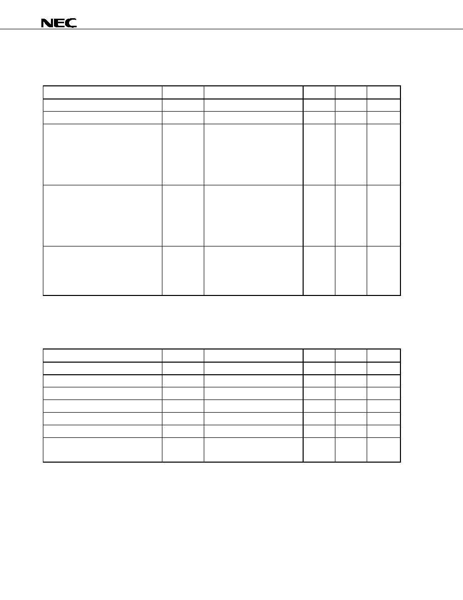
1. PIN INFORMATION
(1/2)
Pin Name
I/O
Buffer Type
Active
Level
Function
AD (31 : 0)
I/O
5 V PCI I/O
PCI "AD [31 : 0]" signal
CBE (3 : 0)0
I/O
5 V PCI I/O
PCI "C/BE [3 : 0]" signal
PAR
I/O
5 V PCI I/O
PCI "PAR" signal
FRAME0
I/O
5 V PCI I/O
PCI "FRAME#" signal
IRDY0
I/O
5 V PCI I/O
PCI "IRDY#" signal
TRDY0
I/O
5 V PCI I/O
PCI "TRDY#" signal
STOP0
I/O
5 V PCI I/O
PCI "STOP#" signal
IDSEL
I
5 V PCI input
PCI "IDSEL" signal
DEVSEL0
I/O
5 V PCI I/O
PCI "DEVSEL#" signal
REQ0
O
5 V PCI output
PCI "REQ#" signal
GNT0
I
5 V PCI input
PCI "GNT#" signal
PERR0
I/O
5 V PCI I/O
PCI "PERR#" signal
SERR0
O
5 V PCI N-ch open drain
PCI "SERR#" signal
INTA0
O
5 V PCI N-ch open drain
Low
PCI "INTA#" signal
INTB0
O
5 V PCI N-ch open drain
Low
PCI "INTB#" signal
INTC0
O
5 V PCI N-ch open drain
Low
PCI "INTC#" signal
PCLK
I
5 V PCI input
PCI "CLK" signal
VBBRST0
I
5 V tolerant input
Low
Hardware reset for chip
CRUN0
I/O
5 V PCI I/O
PCI "CLKRUN#" signal
PME0
O
5 V PCI N-ch open drain
Low
PCI "PME#" signal
VCCRST0
I
5 V tolerant input
Low
Reset for power management
SMI0
O
5 V tolerant N-ch open drain
Low
System management interrupt output
XT1/SCLK
I
Input
System clock input or oscillator in
XT2 O
Output
oscillator
out
DP (5 : 1)
I/O
USB high speed D
+ I/O
USB high speed D
+ signal
DM (5 : 1)
I/O
USB high speed D
- I/O
USB high speed D
- signal
RSDP (5 : 1)
O
USB full speed D
+ Output
USB full speed D
+ signal
RSDM (5 : 1)
O
USB full speed D
- Output
USB full speed D
- signal
OCI (5 : 1)
I (I/O)
Input
Low
USB root hub port's overcurrent status input
PPON (5 : 1)
O (I/O)
Output
High
USB root hub port's power supply control output
LEGC
I (I/O)
Input
High
Legacy support switch
SRCLK
O
Output
Serial ROM clock out
SRDTA
I/O
I/O
Serial ROM data
SRMOD
I
Input with 50 k
pull down R
High
Serial ROM input enable
RREF A
Analog
Reference
resistor
NTEST1
I
Input with 12 k
pull down R
High
Test pin
Data Sheet S16265EJ4V0DS
9
µ
PD720101
(2/2)
Pin Name
I/O
Buffer Type
Active
Level
Function
SMC
I
Input with 50 k
pull down R
High
Scan mode control
TEB
I
Input with 50 k
pull down R
High
BIST enable
AMC
I
Input with 50 k
pull down R
High
ATG mode control
TEST
I
Input with 50 k
pull down R
High
Test control
NANDTEST
I
Input with 50 k
pull down R
High
NAND tree test enable
AV
DD
V
DD
for analog circuit
V
DD
V
DD
V
DD_PCI
5 V (5 V PCI) or 3.3 V (3.3 V PCI)
AV
SS
V
SS
for analog circuit
V
SS
V
SS
N.C.
No
connection
Remarks 1. "5 V tolerant" means that the buffer is 3 V buffer with 5 V tolerant circuit.
2. "5 V PCI" indicates a PCI buffer, which complies with the 3 V PCI standard, has a 5 V tolerant circuit. It
does not indicate that this buffer fully complies with 5 V PCI standard. However, this function can be
used for evaluating the operation of a device on a 5 V add-in card.
3. The signal marked as "(I/O)" in the above table operates as I/O signals during testing. However, they
do not need to be considered in normal use.

Data Sheet S16265EJ4V0DS
10
µ
PD720101
2. HOW TO CONNECT TO EXTERNAL ELEMENTS
2.1
Handling Unused Pins
To realize less than 5 ports host controller implementation, appropriate value shall be set to Port No field in EXT1
register. And unused pins shall be connected as shown below.
Pin Direction
Connection
Method
DPx
I/O
Tied to "low".
DMx
I/O
Tied to "low".
RSDPx
O
No connection (Open)
RSDMx
O
No connection (Open)
OCIx I
"H"
clamp
PPONx
O
No connection (Open)
2.2
USB Port Connection
Figure 2-1. USB Downstream Port Connection
Inside-package
DP
DM
RSDP
RSDM
R
S
= 36
±
1%
15 k
±
5%
Port: D+
Outside-package
Port: D-
R
S
+ R
on
(resistance for driver which is active) = 45
±
10%
ground
R
S
= 36
±
1%

Data Sheet S16265EJ4V0DS
11
µ
PD720101
2.3
PLL Capacitor Connection
Figure 2-2. RREF Connection
Inside-package
AV
SS
(R)
RREF
9.1 k
±
1%
Outside-package
2.4 X'tal
Connection
Figure 2-3. X'tal Connection
Inside-package
XT1/SCLK
V
SS
XT2
Outside-package
V
SS
C1
X'tal
C2
R
The following crystals are evaluated on our reference design board. Table 2-1 shows the external parameters.

Data Sheet S16265EJ4V0DS
12
µ
PD720101
Table 2-1. External Parameters
Vender X'tal R
C1
C2
KDS
Note 1
AT-49 30.000 MHz
100
12 pF
10 pF
NDK
Note 2
AT-41 30.000 MHz
100
10 pF
10 pF
AT-41CD2 30.000 MHz
100
10 pF
10 pF
NX3225DA 30.000 MHz
100
10 pF
10 pF
NX5032GA
30.000
MHz
100
10 pF
10 pF
NX8045GB
30.000
MHz
100
10 pF
10 pF
Notes 1. DAISHINKU CORP.
2. NIHON DEMPA KOGYO CO., LTD.
In using these crystals, contact KDS or NDK to get the specification on external components to be used in
conjunction with the crystal.
KDS's home page: http://www.kdsj.co.jp
NDK's home page: http://www.ndk-j.co.jp
2.5
External Serial ROM Connection
Figure 2-4. External Serial ROM Connection
SRCLK
SRDTA
1.5 k
External serial ROM
3.3 V
SCL
SDA
A
1
SRMOD
A
0
A
2
GND
V
DD
WP
Inside-package
Outside-package
C
These pins for external serial ROM can be opened, when serial ROM is not necessary on board.

Data Sheet S16265EJ4V0DS
13
µ
PD720101
3. ELECTRICAL SPECIFICATIONS
3.1 Buffer
List
∑ 3 V input buffer with pull down resistor
NTEST1, TEST, SRMOD, NANDTEST, SMC, AMC, TEB
∑ 3 V PCI I
OL
= 9 mA 3-state output buffer
PPON(5:1), SRCLK
∑ 3 V I
OL
= 9 mA bi-directional buffer
LEGC, SRDTA
∑ 3 V I
OL
= 9 mA bi-directional buffer with enable (OR type)
OCI(5:1)
∑ 3 V oscillator interface
XT1/SCLK, XT2
∑ 5 V input buffer
VBBRST0, VCCRST0
∑ 5 V I
OL
= 12 mA N-ch open drain buffer
SMI0, PME0, INTA0, INTB0, INTC0, SERR0
∑ 5 V PCI input buffer with enable (OR type)
PCLK, GNT0, IDSEL
∑ 5 V PCI I
OL
= 12 mA 3-state output buffer
REQ0
∑ 5 V PCI I
OL
= 9 mA bi-directional buffer with input enable (OR-type)
AD(31:0), CBE(3:0)0, PAR, FRAME0, IRDY0, TRDY0, STOP0, DEVSEL0, PERR0, CRUN0
∑ USB interface, analog signal
DP(5:1), DM(5:1), RSDP(5:1), RSDM(5:1), RREF
Above, "5 V" refers to a 3 V buffer with 5 V tolerant circuit. Therefore, it is possible to have a 5 V connection for an
external bus, but the output level will be only up to 3 V, which is the V
DD
voltage. Similarly, "5 V PCI" above refers to a
PCI buffer that has a 5 V tolerant circuit, which meets the 3 V PCI standard; it does not refer to a PCI buffer that
meets the 5 V PCI standard.

Data Sheet S16265EJ4V0DS
14
µ
PD720101
3.2 Terminology
Terms Used in Absolute Maximum Ratings
Parameter Symbol
Meaning
Power supply voltage
V
DD
, AV
DD
,
V
DD_PCI
Indicates voltage range within which damage or reduced reliability will not
result when power is applied to a V
DD
pin.
Input voltage
V
I
Indicates voltage range within which damage or reduced reliability will not
result when power is applied to an input pin.
Output voltage
V
O
Indicates voltage range within which damage or reduced reliability will not
result when power is applied to an output pin.
Operating ambient temperature
T
A
Indicates the ambient temperature range for normal logic operations.
Storage temperature
T
stg
Indicates the element temperature range within which damage or reduced
reliability will not result while no voltage or current are applied to the device.
Terms Used in Recommended Operating Range
Parameter Symbol
Meaning
Power supply voltage
V
DD
, AV
DD
,
V
DD_PCI
Indicates the voltage range for normal logic operations occur when V
SS
= 0
V.
High-level input voltage
V
IH
Indicates the voltage, which is applied to the input pins of the device, is the
voltage indicates that the high level states for normal operation of the input
buffer.
* If a voltage that is equal to or greater than the "Min." value is applied, the
input voltage is guaranteed as high level voltage.
Low-level input voltage
V
IL
Indicates the voltage, which is applied to the input pins of the device, is the
voltage indicates that the low level states for normal operation of the input
buffer.
* If a voltage that is equal to or lesser than the "Max." value is applied, the
input voltage is guaranteed as low level voltage.
Terms Used in DC Characteristics
Parameter Symbol
Meaning
Off-state output leakage current
I
OZ
Indicates the current that flows from the power supply pins when the rated
power supply voltage is applied when a 3-state output has high impedance.
Output short circuit current
I
OS
Indicates the current that flows when the output pin is shorted (to GND pins)
when output is at high-level.
Input leakage current
I
I
Indicates the current that flows when the input voltage is supplied to the
input pin.
Low-level output current
I
OL
Indicates the current that flows to the output pins when the rated low-level
output voltage is being applied.
High-level output current
I
OH
Indicates the current that flows from the output pins when the rated high-
level output voltage is being applied.

Data Sheet S16265EJ4V0DS
15
µ
PD720101
3.3 Electrical
Specifications
Absolute Maximum Ratings
Parameter Symbol
Condition
Rating Unit
Power supply voltage
V
DD
-0.5 to +4.6 V
AV
DD
-0.5 to +4.6 V
V
DD_PCI
-0.5 to +6.0 V
Input voltage, 5 V buffer
V
I
3.0
V
V
DD
3.6 V
V
I
< V
DD
+ 3.0 V
-0.5 to +6.6 V
Input voltage, 3.3 V buffer
V
I
3.0
V
V
DD
3.6 V
V
I
< V
DD
+ 0.5 V
-0.5 to +4.6 V
Output voltage, 5 V buffer
V
O
3.0
V
V
DD
3.6 V
V
O
< V
DD
+ 3.0 V
-0.5 to +6.6 V
Output voltage, 3.3 V buffer
V
O
3.0
V
V
DD
3.6 V
V
O
< V
DD
+ 0.5 V
-0.5 to +4.6 V
Operating ambient temperature
T
A
0
to
+70
∞C
Storage temperature
T
stg
-65 to +150
∞C
Caution Product quality may suffer if the absolute maximum rating is exceeded even momentarily for any
parameters. That is, the absolute maximum ratings are rated values at which the product is on the
verge of suffering physical damage, and therefore the product must be used under conditions that
ensure that the absolute maximum ratings are not exceeded.
The ratings and conditions indicated for DC characteristics and AC characteristics represent the
quality assurance range during normal operation.
Recommended Operating Ranges
Parameter Symbol
Condition
Min.
Typ.
Max.
Unit
Operating voltage
V
DD
3.0
3.3
3.6
V
AV
DD
3.0
3.3
3.6 V
V
DD_PCI
In 3.3 V PCI
3.0
3.3
3.6
V
In 5 V PCI
4.75
5.0
5.25
V
High-level input voltage
V
IH
3.3 V high-level input voltage
2.0
V
DD
V
5.0 V high-level input voltage
2.0
5.5
V
Low-level input voltage
V
IL
3.3 V low-level input voltage
0
0.8
V
5.0 V low-level input voltage
0
0.8
V
Data Sheet S16265EJ4V0DS
16
µ
PD720101
DC Characteristics (V
DD
= 3.0 to 3.6 V, T
A
= 0 to
+70∞C)
Control pin block
Parameter Symbol
Condition
Min.
Max.
Unit
Off-state output current
I
OZ
V
O
= V
DD
or V
SS
±10
µ
A
Output short circuit current
I
OS
Note
-250 mA
Low-level output current
I
OL
3.3 V low-level output current
V
OL
= 0.4 V
9.0
mA
3.3 V low-level output current
V
OL
= 0.4 V
3.0
mA
5.0 V low-level output current
V
OL
= 0.4 V
12.0
mA
5.0 V low-level output current
V
OL
= 0.4 V
6.0
mA
High-level output current
I
OH
3.3 V high-level output current
V
OH
= 2.4 V
-9.0 mA
3.3 V high-level output current
V
OH
= 2.4 V
-3.0 mA
5.0 V high-level output current
V
OH
= 2.4 V
-2.0 mA
5.0 V high-level output current
V
OH
= 2.4 V
-2.0 mA
Input leakage current
I
I
3.3 V buffer
V
I
= V
DD
or V
SS
±10
µ
A
3.3 V buffer with 50 k
PD
V
I
= V
DD
191
µ
A
5.0 V buffer
V
I
= V
DD
or V
SS
±10
µ
A
Note
The output short circuit time is one second or less and is only for one pin on the LSI.
PCI interface block
Parameter Symbol
Condition
Min.
Max.
Unit
High-level input voltage
V
IH
2.0
5.25
V
Low-level input voltage
V
IL
0
0.8
V
Low-level output current
I
OL
V
OL
= 0.4 V
12.0
mA
High-level output current
I
OH
V
OH
= 2.4 V
-2.0 mA
Input high leakage current
I
IH
V
IN
= 2.7 V
70
µ
A
Input low leakage current
I
IL
V
IN
= 0.5 V
-70
µ
A
PME0 leakage current
I
OFF
V
O
< 3.6 V
V
CC
off or floating
1
µ
A

Data Sheet S16265EJ4V0DS
17
µ
PD720101
USB interface block
Parameter Symbol
Conditions
Min.
Max.
Unit
Serial resistor between DP (DM) and
RSDP (RSDM)
R
S
35.64
36.36
Output pin impedance
Z
HSDRV
Includes
R
S
resistor
40.5
49.5
Input Levels for Low-/full-speed:
High-level input voltage (drive)
V
IH
2.0
V
High-level input voltage (floating)
V
IHZ
2.7 3.6 V
Low-level input voltage
V
IL
0.8 V
Differential input sensitivity
V
DI
(D+) - (D-) 0.2
V
Differential common mode range
V
CM
Includes
V
DI
range
0.8
2.5
V
Output Levels for Low-/full-speed:
High-level output voltage
V
OH
R
L
of 14.25 k
to GND
2.8
3.6
V
Low-level output voltage
V
OL
R
L
of 1.425 k
to 3.6 V
0.0
0.3
V
SE1 V
OSE1
0.8
V
Output signal crossover point voltage
V
CRS
1.3
2.0 V
Input Levels for High-speed:
High-speed squelch detection threshold
(differential signal)
V
HSSQ
100
150 mV
High-speed disconnect detection
threshold (differential signal)
V
HSDSC
525
625 mV
High-speed data signaling common
mode voltage range
V
HSCM
-50
+500 mV
High-speed differential input signaling
level
See Figure 3-4.
Output Levels for High-speed:
High-speed idle state
V
HSOI
-10
+10 mV
High-speed data signaling high
V
HSOH
360
440 mV
High-speed data signaling low
V
HSOL
-10
+10 mV
Chirp J level (differential signal)
V
CHIRPJ
700
1100 mV
Chirp K level (differential signal)
V
CHIRPK
-900
-500 mV

Data Sheet S16265EJ4V0DS
18
µ
PD720101
Figure 3-1. Differential Input Sensitivity Range for Low-/full-speed
4.6
-
1.0
Input Voltage Range (V)
Differential Input Voltage Range
Differential Output
Crossover
Voltage Range
0.0
0.2
0.4
0.6
0.8
1.0
1.2
1.4
1.6
1.8
2.0
2.2
2.4
2.6
2.8
3.0
3.2
Figure 3-2. Full-speed Buffer V
OH
/I
OH
Characteristics for High-speed Capable Transceiver
Max.
Min.
-
80
-
60
-
40
-
20
0
V
DD
-
0.3
V
OUT
(V)
I
OUT
(mA)
V
DD
-
2.3
V
DD
-
3.3
V
DD
-
0.8
V
DD
V
DD
-
1.3
V
DD
-
1.8
V
DD
-
2.8
Figure 3-3. Full-speed Buffer V
OL
/I
OL
Characteristics for High-speed Capable Transceiver
Max.
Min.
80
60
40
20
0
0
0.5
1
1.5
2
2.5
3
V
OUT
(V)
I
OUT
(mA)

Data Sheet S16265EJ4V0DS
19
µ
PD720101
Figure 3-4. Receiver Sensitivity for Transceiver at DP/DM
0 V
Differential
+
400 mV
Differential
-
400 mV
Differential
Unit Interval
Level 1
Level 2
0%
100%
Point 5
Point 2
Point 1
Point 3
Point 4
Point 6
Figure 3-5. Receiver Measurement Fixtures
Vbus
D+
D-
Gnd
15.8
+
To 50
Inputs of a
High Speed Differential
Oscilloscope, or 50
Outputs of a High Speed
Differential Data Generator
-
50
Coax
50
Coax
USB
Connector
Nearest
Device
Test Supply Voltage
15.8
143
143
Pin capacitance
Parameter Symbol
Condition
Min.
Max.
Unit
Input capacitance
C
I
V
DD
= 0 V, T
A
= 25∞C
6
8
pF
Output capacitance
C
O
f
C
= 1 MHz
10
12
pF
I/O capacitance
C
IO
Unmeasured pins returned to 0
V
10 12 pF
PCI input pin capacitance
C
in
8 pF
PCI clock input pin capacitance
C
clk
6
8 pF
PCI IDSEL input pin capacitance
C
IDSEL
8
pF

Data Sheet S16265EJ4V0DS
20
µ
PD720101
Power consumption
Parameter Symbol
Condition
Typ.
(30 MHz X'tal)
Typ.
(48 MHz OSC)
Unit
Power Consumption
P
WD0-0
Device state = D0, All the ports does not connect to
any function, and each OHCI controller is under
UsbSuspend and EHCI controller is stopped.
Note1
31.4 10.4 mA
P
WD0-2
The power consumption under the state without
suspend. Device state = D0, The number of active
ports is 2.
Note2
Full- or low-speed device(s) is (are) on the port.
High-speed device(s) is (are) on the port.
53.1
204.6
31.9
204.2
mA
mA
P
WD0-3
The power consumption under the state without
suspend. Device state = D0, The number of active
ports is 3.
Note2
Full- or low-speed device(s) is (are) on the port.
High-speed device(s) is (are) on the port.
55.3
253.8
34.2
255.5
mA
mA
P
WD0-4
The power consumption under the state without
suspend. Device state = D0, The number of active
ports is 4.
Note2
Full- or low-speed device(s) is (are) on the port.
High-speed device(s) is (are) on the port.
57.4
301.6
36.7
300.1
mA
mA
P
WD0-5
The power consumption under the state without
suspend. Device state = D0, The number of active
ports is 5.
Note2
Full- or low-speed device(s) is (are) on the port.
High-speed device(s) is (are) on the port.
59.8
349.1
38.8
345.2
mA
mA
P
WD0_C
The power consumption under suspend state during
PCI clock is stopped by CRUN0. Device state = D0.
30.5 10.4 mA
P
WD1
Device state = D1, Analog PLL output is stopped.
Note 3
7.7 10.4 mA
P
WD2
Device state = D2, Analog PLL output is stopped.
Note 3
7.7 10.4 mA
P
WD3H
Device state = D3
hot
, VCCRST0 = High, Analog PLL
output is stopped.
Note 3
7.7 10.4 mA
P
WD3C
Device state = D3
cold
, VCCRST0 = Low.
Note 4
0.03
3.81
mA
Notes 1.
When any device is not connected to all the ports of HC, the power consumption for HC does not depend
on the number of active ports.
2.
The number of active ports is set by the value of Port No Field in PCI configuration space EXT register.
3.
This is the case when PCI bus state is B0.
4.
This is the case when PCI bus state is B3.
Remark
These are estimated value on WindowsTM XP environment.

Data Sheet S16265EJ4V0DS
21
µ
PD720101
System clock ratings
Parameter Symbol
Condition
Min.
Typ.
Max.
Unit
Clock frequency
f
CLK
X'tal
-500
ppm
30
+500
ppm
MHz
Oscillator
block
-500
ppm
48
+500
ppm
MHz
Clock duty cycle
t
DUTY
40 50 60 %
Remarks 1.
Recommended accuracy of clock frequency is
± 100 ppm.
2.
Required accuracy of X'tal or oscillator block is including initial frequency accuracy, the spread of X'tal
capacitor loading, supply voltage, temperature, and aging, etc.

Data Sheet S16265EJ4V0DS
22
µ
PD720101
AC Characteristics (V
DD
= 3.0 to 3.6 V, T
A
= 0 to
+70∞C)
PCI interface block
Parameter Symbol
Condition
Min.
Max.
Unit
PCI clock cycle time
t
cyc
30
ns
PCI clock pulse, high-level width
t
high
11
ns
PCI clock pulse, low-level width
t
low
11
ns
PCI clock, rise slew rate
S
cr
0.2V
DD
to 0.6V
DD
1
4
V/ns
PCI clock, fall slew rate
S
cf
0.2V
DD
to 0.6V
DD
1
4
V/ns
PCI reset active time (vs. power supply
stability)
t
rst
1
ms
PCI reset active time (vs. CLK start)
t
rst-clk
100
µ
s
Output float delay time (vs. RST0
) t
rst-off
40
ns
PCI reset rise slew rate
S
rr
50
mV/ns
PCI bus signal output time (vs. PCLK
) t
val
2
11
ns
PCI point-to-point signal output time (vs.
PCLK
)
t
val
(ptp)
REQ0
2
12
ns
Output delay time (vs. PCLK
) t
on
2
ns
Output float delay time (vs. PCLK
) t
off
28
ns
Input setup time (vs. PCLK
) t
su
7
ns
Point-to-point input setup time (vs.
PCLK
)
t
su
(ptp)
GNT0
10
ns
Input hold time
t
h
0
ns

Data Sheet S16265EJ4V0DS
23
µ
PD720101
USB interface block
(1/2)
Parameter Symbol
Conditions
Min.
Max.
Unit
Low-speed Source Electrical Characteristics
Rise time (10 to 90%)
t
LR
C
L
= 200 to 600 pF,
R
S
= 36
75 300
ns
Fall time (90 to 10%)
t
LF
C
L
= 200 to 600 pF,
R
S
= 36
75 300
ns
Differential rise and fall time matching
t
LRFM
(t
LR
/t
LF
) 80
125
%
Low-speed data rate
t
LDRATHS
Average bit rate
1.49925
1.50075
Mbps
Source jitter total (including frequency
tolerance):
To next transition
For paired transitions
t
DDJ1
t
DDJ2
-25
-14
+25
+14
ns
ns
Source jitter for differential transition to
SE0 transition
t
LDEOP
-40
+100 ns
Receiver jitter:
To next transition
For paired transitions
t
UJR1
t
UJR2
-152
-200
+152
+200
ns
ns
Source SE0 interval of EOP
t
LEOPT
1.25
1.50
µ
s
Receiver SE0 interval of EOP
t
LEOPR
670
ns
Width of SE0 interval during differential
transition
t
FST
210 ns
Full-speed Source Electrical Characteristics
Rise time (10 to 90%)
t
FR
C
L
= 50 pF,
R
S
= 36
4 20
ns
Fall time (90 to 10%)
t
FF
C
L
= 50 pF,
R
S
= 36
4 20
ns
Differential rise and fall time matching
t
FRFM
(t
FR
/t
FF
) 90
111.11
%
Full-speed data rate
t
FDRATHS
Average bit rate
11.9940
12.0060
Mbps
Frame interval
t
FRAME
0.9995 1.0005 ms
Consecutive frame interval jitter
t
RFI
No clock adjustment
42
ns
Source jitter total (including frequency
tolerance):
To next transition
For paired transitions
t
DJ1
t
DJ2
-3.5
-4.0
+3.5
+4.0
ns
ns
Source jitter for differential transition to
SE0 transition
t
FDEOP
-2
+5 ns
Receiver jitter:
To next transition
For paired transitions
t
JR1
t
JR2
-18.5
-9
+18.5
+9
ns
ns
Source SE0 interval of EOP
t
FEOPT
160
175 ns
Receiver SE0 interval of EOP
t
FEOPR
82
ns
Width of SE0 interval during differential
transition
t
FST
14 ns

Data Sheet S16265EJ4V0DS
24
µ
PD720101
(2/2)
Parameter Symbol
Conditions
Min.
Max.
Unit
High-speed Source Electrical Characteristics
Rise time (10 to 90%)
t
HSR
500
ps
Fall time (90 to 10%)
t
HSF
500
ps
Driver waveform
See Figure 3-6.
High-speed data rate
t
HSDRAT
479.760 480.240 Mbps
Microframe interval
t
HSFRAM
124.9375 125.0625
µ
s
Consecutive microframe interval difference
t
HSRFI
4
high-
speed
Bit
times
Data source jitter
See Figure 3-6.
Receiver jitter tolerance
See Figure 3-4.
Hub Event Timings
Time to detect a downstream facing port
connect event
t
DCNN
2.5
2000
µ
s
Time to detect a disconnect event at a
hub's downstream facing port
t
DDIS
2.0
2.5
µ
s
Duration of driving resume to a
downstream port
t
DRSMDN
Nominal
20
ms
Time from detecting downstream resume
to rebroadcast
t
URSM
1.0 ms
Inter-packet delay for packets traveling in
same direction for high-speed
t
HSIPDSD
88
Bit
times
Inter-packet delay for packets traveling in
opposite direction for high-speed
t
HSIPDOD
8
Bit
times
Inter-packet delay for root hub response for
high-speed
t
HSRSPIPD1
192
Bit
times
Time for which a Chirp J or Chirp K must
be continuously detected during reset
handshake
t
FILT
2.5
µ
s
Time after end of device Chirp K by which
hub must start driving first Chirp K
t
WTDCH
100
µ
s
Time for which each individual Chirp J or
Chirp K in the chirp sequence is driven
downstream during reset
t
DCHBIT
40
60
µ
s
Time before end of reset by which a hub
must end its downstream chirp sequence
t
DCHSE0
100
500
µ
s

Data Sheet S16265EJ4V0DS
25
µ
PD720101
Figure 3-6. Transmit Waveform for Transceiver at DP/DM
0 V
Differential
+
400 mV
Differential
-
400 mV
Differential
Unit Interval
Level 1
Level 2
0%
100%
Point 4
Point 3
Point 1
Point 2
Point 5
Point 6
Figure 3-7. Transmitter Measurement Fixtures
Vbus
D+
D-
Gnd
15.8
+
To 50
Inputs of a
High Speed Differential
Oscilloscope, or 50
Outputs of a High Speed
Differential Data Generator
-
50
Coax
50
Coax
USB
Connector
Nearest
Device
Test Supply Voltage
15.8
143
143

Data Sheet S16265EJ4V0DS
26
µ
PD720101
3.4 Timing
Diagram
PCI clock
0.4V
DD
0.6V
DD
0.2V
DD
0.5V
DD
0.3V
DD
0.4V
DD
(ptp:min)
t
cyc
t
high
t
low
PCI reset
PCLK
PWR_GOOD
VBBRST0
100 ms (typ.)
t
rst
t
rst-off
PCI Signals
Valid
t
rst-clk

Data Sheet S16265EJ4V0DS
27
µ
PD720101
PCI output timing measurement condition
PCLK
0.4V
DD
0.6V
DD
0.2V
DD
Output delay
Output
0.615V
DD
(for falling edge)
0.285V
DD
(for falling edge)
t
val
, t
val
(ptp)
t
on
t
off
PCI input timing measurement condition
PCLK
0.4V
DD
0.6V
DD
0.2V
DD
Input
t
su
, t
su
(ptp)
0.6V
DD
0.2V
DD
0.4V
DD
t
h

Data Sheet S16265EJ4V0DS
28
µ
PD720101
USB differential data jitter for full-speed
t
PERIOD
Differential
Data Lines
Crossover
Points
Consecutive
Transitions
N
◊
t
PERIOD
+
t
xDJ1
Paired
Transitions
N
◊
t
PERIOD
+
t
xDJ2
USB differential-to-EOP transition skew and EOP width for low-/full-speed
t
PERIOD
Differential
Data Lines
Crossover
Point
Crossover
Point Extended
Source EOP Width: t
FEOPT
t
LEOPT
Receiver EOP Width: t
FEOPR
t
LEOPR
Diff. Data-to-
SE0 Skew
N
◊
t
PERIOD
+
t
xDEOP
USB receiver jitter tolerance for low-/full-speed
Differential
Data Lines
t
PERIOD
t
xJR
t
xJR1
t
xJR2
Consecutive
Transitions
N
◊
t
PERIOD
+
t
xJR1
Paired
Transitions
N
◊
t
PERIOD
+
t
xJR2

Data Sheet S16265EJ4V0DS
29
µ
PD720101
Low-/full-speed disconnect detection
D
-
/D
+
D
+
/D
-
V
IZH
(min)
V
IL
V
SS
Device
Disconnected
Disconnect
Detected
t
DDIS
Full-/high-speed device connect detection
V
IH
V
SS
Device
Connected
Connect
Detected
D
-
D
+
t
DCNN
Low-speed device connect detection
V
IH
V
SS
Device
Connected
Connect
Detected
D
+
D
-
t
DCNN

Data Sheet S16265EJ4V0DS
30
µ
PD720101
4. PACKAGE DRAWINGS
108
73
1
36
109
144
72
37
144-PIN PLASTIC LQFP (FINE PITCH) (20x20)
ITEM
MILLIMETERS
NOTE
A
22.0
±
0.2
B
20.0
±
0.2
C
20.0
±
0.2
D
F
1.25
22.0
±
0.2
S144GJ-50-UEN
S
1.5
±
0.1
K
1.0
±
0.2
L
0.5
±
0.2
R
3
∞+
4
∞
-
3
∞
G
1.25
H
0.22
±
0.05
I
0.08
J
0.5 (T.P.)
M
0.17
N
0.08
P
1.4
Q
0.10
±
0.05
+
0.03
-
0.07
Each lead centerline is located within 0.08 mm of
its true position (T.P.) at maximum material condition.
S
S
M
detail of lead end
I
J
F
G
H
Q
R
P
K
M
L
N
C
D
S
A
B

Data Sheet S16265EJ4V0DS
31
µ
PD720101
14
13
12
11
10
9
8
7
6
5
4
3
2
1
N
P
M L K J H G F E D C B A
E
A
B
ZD
ZE
S
A2
A
A1
ITEM
MILLIMETERS
D
E
w
A
A1
A2
e
b
x
y
y1
ZD
ZE
12.00
±
0.10
12.00
±
0.10
0.80
0.08
0.10
0.20
0.80
0.80
0.20
0.35
±
0.06
1.48
±
0.10
1.13
P144F1-80-EA8
0.50+0.05
≠0.10
144-PIN PLASTIC FBGA (12x12)
S
w
A
S
w
B
y1
S
S
y
e
S
x
b
A B
M
INDEX MARK
D

Data Sheet S16265EJ4V0DS
32
µ
PD720101
5. RECOMMENDED SOLDERING CONDITIONS
The
µ
PD720101 should be soldered and mounted under the following recommended conditions.
For soldering methods and conditions other than those recommended below, contact an NEC Electronics sales
representative.
For technical information, see the following website.
Semiconductor Device Mount Manual (http://www.necel.com/pkg/en/mount/index.html)
µ
PD720101GJ-UEN: 144-pin plastic LQFP (Fine pitch) (20
◊ 20)
Soldering Method
Soldering Conditions
Symbol
Infrared reflow
Package peak temperature: 235∞C, Time: 30 seconds max. (at 210∞C or higher),
Count: Three times or less
Exposure limit: 3 days
Note
(after that, prebake at 125∞C for 10 hours)
IR35-103-3
Partial heating
Pin temperature: 300∞C max., Time: 3 seconds max. (per pin row)
≠
Note
After opening the dry pack, store it at 25∞C or less and 65% RH or less for the allowable storage period.
µ
PD720101F1-EA8: 144-pin plastic FBGA (12
◊ 12)
Soldering Method
Soldering Conditions
Symbol
Infrared reflow
Package peak temperature: 235∞C, Time: 30 seconds max. (at 210∞C or higher),
Count: Three times or less
Exposure limit: 7 days
Note
(after that, prebake at 125∞C for 10 hours)
IR35-107-3
Note
After opening the dry pack, store it at 25∞C or less and 65% RH or less for the allowable storage period.

Data Sheet S16265EJ4V0DS
33
µ
PD720101
[MEMO]

Data Sheet S16265EJ4V0DS
34
µ
PD720101
[MEMO]

Data Sheet S16265EJ4V0DS
35
µ
PD720101
1
2
3
4
VOLTAGE APPLICATION WAVEFORM AT INPUT PIN
Waveform distortion due to input noise or a reflected wave may cause malfunction. If the input of the
CMOS device stays in the area between V
IL
(MAX) and V
IH
(MIN) due to noise, etc., the device may
malfunction. Take care to prevent chattering noise from entering the device when the input level is fixed,
and also in the transition period when the input level passes through the area between V
IL
(MAX) and
V
IH
(MIN).
HANDLING OF UNUSED INPUT PINS
Unconnected CMOS device inputs can be cause of malfunction. If an input pin is unconnected, it is
possible that an internal input level may be generated due to noise, etc., causing malfunction. CMOS
devices behave differently than Bipolar or NMOS devices. Input levels of CMOS devices must be fixed
high or low by using pull-up or pull-down circuitry. Each unused pin should be connected to V
DD
or GND
via a resistor if there is a possibility that it will be an output pin. All handling related to unused pins must
be judged separately for each device and according to related specifications governing the device.
PRECAUTION AGAINST ESD
A strong electric field, when exposed to a MOS device, can cause destruction of the gate oxide and
ultimately degrade the device operation. Steps must be taken to stop generation of static electricity as
much as possible, and quickly dissipate it when it has occurred. Environmental control must be
adequate. When it is dry, a humidifier should be used. It is recommended to avoid using insulators that
easily build up static electricity. Semiconductor devices must be stored and transported in an anti-static
container, static shielding bag or conductive material. All test and measurement tools including work
benches and floors should be grounded. The operator should be grounded using a wrist strap.
Semiconductor devices must not be touched with bare hands. Similar precautions need to be taken for
PW boards with mounted semiconductor devices.
STATUS BEFORE INITIALIZATION
Power-on does not necessarily define the initial status of a MOS device. Immediately after the power
source is turned ON, devices with reset functions have not yet been initialized. Hence, power-on does
not guarantee output pin levels, I/O settings or contents of registers. A device is not initialized until the
reset signal is received. A reset operation must be executed immediately after power-on for devices
with reset functions.
NOTES FOR CMOS DEVICES
Purchase of NEC Electronics l
2
C components conveys a license under the Philips l
2
C Patent Rights to
use these components in an l
2
C system, provided that the system conforms to the l
2
C Standard
Specification as defined by Philips.

µ
PD720101
USB logo is a trademark of USB Implementers Forum, Inc.
Windows is either a registered trademark or a trademark of Microsoft Corporation in the United States
and/or other countries.
The information in this document is current as of June, 2004. The information is subject to change
without notice. For actual design-in, refer to the latest publications of NEC Electronics data sheets or
data books, etc., for the most up-to-date specifications of NEC Electronics products. Not all
products and/or types are available in every country. Please check with an NEC Electronics sales
representative for availability and additional information.
No part of this document may be copied or reproduced in any form or by any means without the prior
written consent of NEC Electronics. NEC Electronics assumes no responsibility for any errors that may
appear in this document.
NEC Electronics does not assume any liability for infringement of patents, copyrights or other intellectual
property rights of third parties by or arising from the use of NEC Electronics products listed in this document
or any other liability arising from the use of such products. No license, express, implied or otherwise, is
granted under any patents, copyrights or other intellectual property rights of NEC Electronics or others.
Descriptions of circuits, software and other related information in this document are provided for illustrative
purposes in semiconductor product operation and application examples. The incorporation of these
circuits, software and information in the design of a customer's equipment shall be done under the full
responsibility of the customer. NEC Electronics assumes no responsibility for any losses incurred by
customers or third parties arising from the use of these circuits, software and information.
While NEC Electronics endeavors to enhance the quality, reliability and safety of NEC Electronics products,
customers agree and acknowledge that the possibility of defects thereof cannot be eliminated entirely. To
minimize risks of damage to property or injury (including death) to persons arising from defects in NEC
Electronics products, customers must incorporate sufficient safety measures in their design, such as
redundancy, fire-containment and anti-failure features.
NEC Electronics products are classified into the following three quality grades: "Standard", "Special" and
"Specific".
The "Specific" quality grade applies only to NEC Electronics products developed based on a customer-
designated "quality assurance program" for a specific application. The recommended applications of an NEC
Electronics product depend on its quality grade, as indicated below. Customers must check the quality grade of
each NEC Electronics product before using it in a particular application.
The quality grade of NEC Electronics products is "Standard" unless otherwise expressly specified in NEC
Electronics data sheets or data books, etc. If customers wish to use NEC Electronics products in applications
not intended by NEC Electronics, they must contact an NEC Electronics sales representative in advance to
determine NEC Electronics' willingness to support a given application.
(Note)
∑
∑
∑
∑
∑
∑
M8E 02. 11-1
(1)
(2)
"NEC Electronics" as used in this statement means NEC Electronics Corporation and also includes its
majority-owned subsidiaries.
"NEC Electronics products" means any product developed or manufactured by or for NEC Electronics (as
defined above).
Computers, office equipment, communications equipment, test and measurement equipment, audio
and visual equipment, home electronic appliances, machine tools, personal electronic equipment
and industrial robots.
Transportation equipment (automobiles, trains, ships, etc.), traffic control systems, anti-disaster
systems, anti-crime systems, safety equipment and medical equipment (not specifically designed
for life support).
Aircraft, aerospace equipment, submersible repeaters, nuclear reactor control systems, life
support systems and medical equipment for life support, etc.
"Standard":
"Special":
"Specific":