 | –≠–ª–µ–∫—Ç—Ä–æ–Ω–Ω—ã–π –∫–æ–º–ø–æ–Ω–µ–Ω—Ç: SN74LS395 | –°–∫–∞—á–∞—Ç—å:  PDF PDF  ZIP ZIP |
5-551
FAST AND LS TTL DATA
4-BIT SHIFT REGISTER
WITH 3-STATE OUTPUTS
The SN74LS395 is a 4-Bit Register with 3-state outputs and can operate
in either a synchronous parallel load or a serial shift-right mode, as
determined by the Select input. An asynchronous active LOW Master Reset
(MR) input overrides the synchronous operations and clears the register. An
active HIGH Output Enable (OE) input controls the 3-state output buffers, but
does not interfere with the other operations. The fourth stage also has a
conventional output for linking purposes in multi-stage serial operations.
∑
Shift Left or Parallel 4-Bit Register
∑
3-State Outputs
∑
Input Clamp Diodes Limit High-Speed Termination Effects
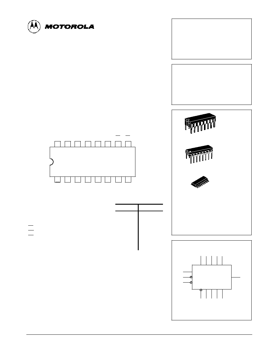
CONNECTION DIAGRAM DIP (TOP VIEW)
14
13
12
11
10
9
1
2
3
4
5
6
7
16
15
8
VCC
MR
O0 O1
O2
O3
CP
Q3
OE
DS
P0
P1
P2
P3
S
GND
PIN NAMES
LOADING (Note a)
HIGH
LOW
P0 ≠ P3
DS
S
CP
MR
OE
O0 ≠ O3
Q3
Parallel Inputs
Serial Data Input
Mode Select Input
Clock (Active LOW) Input
Master Reset (Active LOW) Input
Output Enable (Active HIGH) Input
3-State Register Outputs
Register Output
0.5 U.L.
0.5 U.L.
0.5 U.L.
0.5 U.L.
0.5 U.L.
0.5 U.L.
65 U.L.
10 U.L.
0.25 U.L.
0.25 U.L.
0.25 U.L.
0.25 U.L.
0.25 U.L.
0.25 U.L.
15 U.L.
5 U.L.
NOTES:
a) 1 TTL Unit Load (U.L.) = 40
µ
A HIGH/1.6 mA LOW.
SN74LS395
4-BIT SHIFT REGISTER
WITH 3-STATE OUTPUTS
LOW POWER SCHOTTKY
ORDERING INFORMATION
SN74LSXXXJ
Ceramic
SN74LSXXXN
Plastic
SN74LSXXXD
SOIC
J SUFFIX
CERAMIC
CASE 620-09
N SUFFIX
PLASTIC
CASE 648-08
16
1
16
1
16
1
D SUFFIX
SOIC
CASE 751B-03
LOGIC SYMBOL
VCC = PIN 16
GND = PIN 8
1
2
3 4 5 6
10
9
15 14 13 12
11
7
S P0 P1 P2 P3
DS
CP
OE
MR O0 O1 O2 O3
Q3
5-552
FAST AND LS TTL DATA
SN74LS395
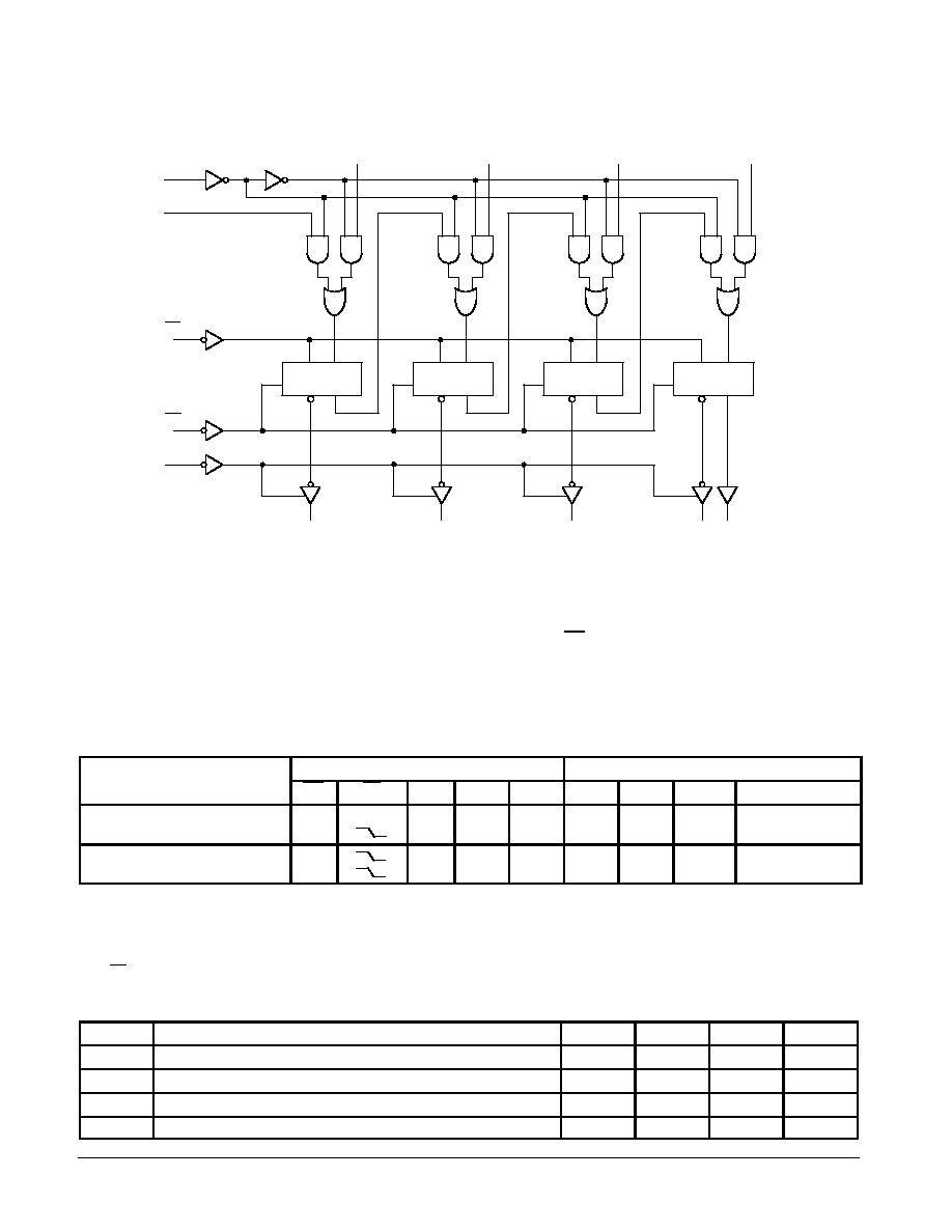
LOGIC DIAGRAM
S
Ds
CP
MR
OE
P0
P1
P2
P3
O0
O1
O2
O3 Q3
CP D
CD
Q
CP D
CD
Q
CP D
CD
Q
CP D
CD
Q
FUNCTION DESCRIPTION
The SN74LS395 contains four D-type edge-triggered
flip-flops and auxiliary gating to select a D input either from a
Parallel (Pn) input or from the preceding stage. When the
Select input is HIGH, the Pn inputs are enabled. A LOW signal
on the S input enables the serial inputs for shift-right opera-
tions, as indicated in the Truth Table.
State changes are initiated by HIGH-to-LOW transitions on
the Clock Pulse (CP) input. Signals on the Pn, Ds and S inputs
can change when the Clock is in either state, provided that the
recommended set-up and hold times are observed. When the
S input is LOW, a CP HIGH-LOW transition transfers data in
Q0 to Q1, Q1 to Q2, and Q2 to Q3. A left-shift is accomplished
by connecting the outputs back to the Pn inputs, but offset one
place to the left, i.e., O3 to P2, O2 to P1 and O1 to P0, with P3
acting as the linking input from another package.
When the OE input is HIGH, the output buffers are disabled
and the Q0≠Q3 outputs are in a high impedance condition.
The shifting, parallel loading or resetting operations can still be
accomplished, however.
MODE SELECT -- TRUTH TABLE
Inputs @ tn
Outputs @ tn+1
Operating Mode
MR
CP
S
Ds
Pn
O0
O1
O2
O3
Asynchronous Reset
L
X
X
X
X
L
L
L
L
Shift, SET First Stage
H
L
H
X
H
O0n
O1n
O2n
Shift, RESET First Stage
H
L
L
X
L
O0n
O1n
O2n
Parallel Load
H
H
X
Pn
P0
P1
P2
P3
H = HIGH Voltage Level
L = LOW Voltage Level
X = Immaterial
tn, n + 1 = time before and after CP HIGH-to-LOW transition
NOTE:
When OE is HIGH, outputs O0 ≠ O3 are in the high impedance state; however, this does not affect other operations or the Q3 output.
GUARANTEED OPERATING RANGES
Symbol
Parameter
Min
Typ
Max
Unit
VCC
Supply Voltage
4.75
5.0
5.25
V
TA
Operating Ambient Temperature Range
0
25
70
∞
C
IOH
Output Current -- High
≠ 0.4
mA
IOL
Output Current -- Low
8.0
mA

5-553
FAST AND LS TTL DATA
SN74LS395
DC CHARACTERISTICS OVER OPERATING TEMPERATURE RANGE
(unless otherwise specified)
Symbol
Parameter
Limits
Unit
Test Conditions
Symbol
Parameter
Min
Typ
Max
Unit
Test Conditions
VIH
Input HIGH Voltage
2.0
V
Guaranteed Input HIGH Voltage for
All Inputs
VIL
Input LOW Voltage
0.8
V
Guaranteed Input LOW Voltage for
All Inputs
VIK
Input Clamp Diode Voltage
≠ 0.65
≠ 1.5
V
VCC = MIN, IIN = ≠ 18 mA
VOH
Output HIGH Voltage
2.7
3.5
V
VCC = MIN, IOH = MAX, VIN = VIH
or VIL per Truth Table
VOL
Output LOW Voltage
0.25
0.4
V
IOL = 4.0 mA
VCC = VCC MIN,
VIN = VIL or VIH
per Truth Table
VOL
Output LOW Voltage
0.35
0.5
V
IOL = 8.0 mA
VIN = VIL or VIH
per Truth Table
IOZH
Output Off Current HIGH
20
µ
A
VCC = MAX, VO = 2.4 V
IOZL
Output Off Current LOW
≠ 20
µ
A
VCC = MAX, VO = 0.4 V
IIH
Input HIGH Current
20
µ
A
VCC = MAX, VIN = 2.7 V
IIH
Input HIGH Current
≠ 0.1
mA
VCC = MAX, VIN = 7.0 V
IIL
Input LOW Current
≠ 0.4
mA
VCC = MAX, VIN = 0.4 V
IOS
Short Circuit Current (Note 1)
≠ 20
≠ 100
mA
VCC = MAX
ICC
Power Supply Current
Total, Output HIGH
31
mA
VCC = MAX, OE = GND, CP = GND
ICC
Total, Output LOW
34
mA
VCC = MAX, OE = 4.5 V, CP
momentary 3.0 V then GND
Note 1: Not more than one output should be shorted at a time, nor for more than 1 second.
AC CHARACTERISTICS
(TA = 25
∞
C)
Symbol
Parameter
Limits
Unit
Test Conditions
Symbol
Parameter
Min
Typ
Max
Unit
Test Conditions
fMAX
Maximum Input Clock Frequency
30
45
MHz
VCC = 5.0 V
CL = 15 pF
tPHL
Propagation Delay, Clear to Output
22
35
ns
VCC = 5.0 V
CL = 15 pF
tPLH
tPHL
Propagation Delay, Low to High
Propagation Delay, High to Low
15
25
30
30
ns
VCC = 5.0 V
CL = 15 pF
tPZH
tPZL
Output Enable Time
15
17
25
25
ns
tPLZ
tPHZ
Output Disable Time
12
11
20
17
ns
CL = 5.0 pF
AC SETUP REQUIREMENTS
(TA = 25
∞
C)
Symbol
Parameter
Limits
Unit
Test Conditions
Symbol
Parameter
Min
Typ
Max
Unit
Test Conditions
tW
Clock Pulse Width
16
ns
VCC = 5.0 V
ts
Setup Time, Mode Select
40
ns
VCC = 5.0 V
ts
Setup Time, All Others
20
ns
VCC = 5.0 V
th
Data Hold Time
10
ns

AC WAVEFORMS
The shaded areas indicate when the input is permitted to change for predictable output performance.
*The Data Input is DS for S = LOW and Pn for S = HIGH.
Figure 1
Figure 2
Figure 3
Figure 4
D
CP OR
MR
Q
VE
VOUT
VOUT
VE
1.3 V
1.3 V
1.3 V
1.3 V
1.3 V
tPLH
tPHL
th(L)
th(H)
1.3 V
1.3 V
1.3 V
1.3 V
1.3 V
1.3 V
1.3V
1.3 V
0.5 V
0.5 V
tPZL
tPLZ
VOL
tPZH tPHZ
VOH
*
1/fmax
tW
ts(L)
ts(H)
S
CP
1.3 V
1.3 V
1.3 V
th(L)
th(H)
ts(L)
ts(H)
LOAD SERIAL DATA
SHIFT RIGHT
LOAD PARALLEL DATA
Figure 5
AC LOAD CIRCUIT
SW2
CL*
5 k
SW1
VCC
RL
TO OUTPUT
UNDER TEST
SWITCH POSITIONS
* Includes Jig and Probe Capacitance.
5-554
FAST AND LS TTL DATA
SN74LS395
SYMBOL
SW1
SW2
tPZH
Open
Closed
tPZL
Closed
Open
tPLZ
Closed
Closed
tPHZ
Closed
Closed
5-555
FAST AND LS TTL DATA
MIN
MIN
MAX
MAX
MILLIMETERS
INCHES
DIM
A
B
C
D
F
G
J
K
M
P
R
9.80
3.80
1.35
0.35
0.40
0.19
0.10
0
∞
5.80
0.25
10.00
4.00
1.75
0.49
1.25
0.25
0.25
7
∞
6.20
0.50
0.386
0.150
0.054
0.014
0.016
0.008
0.004
0
∞
0.229
0.010
0.393
0.157
0.068
0.019
0.049
0.009
0.009
7
∞
0.244
0.019
1.27 BSC
0.050 BSC
NOTES:
1. DIMENSIONING AND TOLERANCING PER ANSI
Y14.5M, 1982.
2. CONTROLLING DIMENSION: MILLIMETER.
3. DIMENSION A AND B DO NOT INCLUDE MOLD
PROTRUSION.
4. MAXIMUM MOLD PROTRUSION 0.15 (0.006)
PER SIDE.
5. 751B 01 IS OBSOLETE, NEW STANDARD
751B 03.
1
8
9
16
-A-
-B-
P
16 PL
D
-T-
K
C
G
M
R X 45
∞
F
J
8 PL
SEATING
PLANE
Case 751B-03 D Suffix
16-Pin Plastic
SO-16
B
0.25 (0.010)
M
M
T
0.25 (0.010)
B
A
M
S
S
Case 648-08 N Suffix
16-Pin Plastic
MIN
MIN
MAX
MAX
MILLIMETERS
INCHES
DIM
A
B
C
D
F
G
H
J
K
L
M
S
18.80
6.35
3.69
0.39
1.02
0.21
2.80
7.50
0
∞
0.51
19.55
6.85
4.44
0.53
1.77
0.38
3.30
7.74
10
∞
1.01
0.740
0.250
0.145
0.015
0.040
0.008
0.110
0.295
0
∞
0.020
0.770
0.270
0.175
0.021
0.070
0.015
0.130
0.305
10
∞
0.040
NOTES:
1. DIMENSIONING AND TOLERANCING PER ANSI
Y14.5M, 1982.
2. CONTROLLING DIMENSION: INCH.
3. DIMENSION L" TO CENTER OF LEADS WHEN
FORMED PARALLEL.
4. DIMENSION B" DOES NOT INCLUDE MOLD
FLASH.
5. ROUNDED CORNERS OPTIONAL.
6. 648 01 THRU 07 OBSOLETE, NEW STANDARD
648 08.
2.54 BSC
1.27 BSC
0.100 BSC
0.050 BSC
-A-
B
1
8
9
16
F
H
G
D
16 PL
S
C
-T-
SEATING
PLANE
K
J
M
L
T A
0.25 (0.010)
M
M
Case 620-09 J Suffix
16-Pin Ceramic Dual In-Line
MIN
MIN
MAX
MAX
MILLIMETERS
INCHES
DIM
19.05
6.10
0.39
1.40
0.23
0
∞
0.39
19.55
7.36
4.19
0.53
1.77
0.27
5.08
15
∞
0.88
0.750
0.240
0.015
0.055
0.009
0
∞
0.015
0.770
0.290
0.165
0.021
0.070
0.011
0.200
15
∞
0.035
1.27 BSC
2.54 BSC
7.62 BSC
0.050 BSC
0.100 BSC
0.300 BSC
A
B
C
D
E
F
G
J
K
L
M
N
NOTES:
1. DIMENSIONING AND TOLERANCING PER ANSI
Y14.5M, 1982.
2. CONTROLLING DIMENSION: INCH.
3. DIMENSION L TO CENTER OF LEAD WHEN
FORMED PARALLEL.
4. DIM F MAY NARROW TO 0.76 (0.030) WHERE
THE LEAD ENTERS THE CERAMIC BODY.
5. 620 01 THRU 08 OBSOLETE, NEW STANDARD
620 09.
-B-
-A-
16 PL
-T-
C
D
E
F
G
J
K
M
N
SEATING
PLANE
16 PL
L
16
9
1
8
0.25 (0.010)
T A
M
S
0.25 (0.010)
T B
M
S
5-556
FAST AND LS TTL DATA
Motorola reserves the right to make changes without further notice to any products herein. Motorola makes no warranty, representation or guarantee regarding
the suitability of its products for any particular purpose, nor does Motorola assume any liability arising out of the application or use of any product or circuit,
and specifically disclaims any and all liability, including without limitation consequential or incidental damages. "Typical" parameters can and do vary in different
applications. All operating parameters, including "Typicals" must be validated for each customer application by customer's technical experts. Motorola does
not convey any license under its patent rights nor the rights of others. Motorola products are not designed, intended, or authorized for use as components in
systems intended for surgical implant into the body, or other applications intended to support or sustain life, or for any other application in which the failure of
the Motorola product could create a situation where personal injury or death may occur. Should Buyer purchase or use Motorola products for any such
unintended or unauthorized application, Buyer shall indemnify and hold Motorola and its officers, employees, subsidiaries, affiliates, and distributors harmless
against all claims, costs, damages, and expenses, and reasonable attorney fees arising out of, directly or indirectly, any claim of personal injury or death
associated with such unintended or unauthorized use, even if such claim alleges that Motorola was negligent regarding the design or manufacture of the part.
Motorola and
are registered trademarks of Motorola, Inc. Motorola, Inc. is an Equal Opportunity/Affirmative Action Employer.
Literature Distribution Centers:
USA: Motorola Literature Distribution; P.O. Box 20912; Phoenix, Arizona 85036.
EUROPE: Motorola Ltd.; European Literature Centre; 88 Tanners Drive, Blakelands, Milton Keynes, MK14 5BP, England.
JAPAN: Nippon Motorola Ltd.; 4-32-1, Nishi-Gotanda, Shinagawa-ku, Tokyo 141, Japan.
ASIA PACIFIC: Motorola Semiconductors H.K. Ltd.; Silicon Harbour Center, No. 2 Dai King Street, Tai Po Industrial Estate, Tai Po, N.T., Hong Kong.