Äîêóìåíòàöèÿ è îïèñàíèÿ www.docs.chipfind.ru
Will be replaced by MHVIC910HNR2 end of Q205. N suffix indicates 260°C reflow
capable. The PFP-16 package has had lead-free terminations from its initial release.
MHVIC910HR2
1
RF Device Data
Freescale Semiconductor
921 MHz - 960 MHz SiFET
RF Integrated Power Amplifier
The MHVIC910HR2 integrated circuit is designed for GSM base stations,
uses Freescale's newest High Voltage (26 Volts) LDMOS IC technology, and
contains a three-stage amplifier. Target applications include macrocell (driver
function) and microcell base stations (final stage). The device is in a PFP-16
Power Flat Pack package which gives excellent thermal performances through
a solderable backside contact.
· Typical GSM Performance @ Full Frequency Band
(921-960 MHz), 26 Volts
Output Power -- 40 dBm (CW) @ P1dB
Power Gain -- 39 dB @ P1dB
Efficiency -- 48% @ P1dB
· On-Chip Matching (50 Ohm Input, DC Blocked, >5 Ohm Output)
· Integrated ESD Protection
· Usable Frequency Range -- 921 to 960 MHz
· In Tape and Reel. R2 Suffix = 1,500 Units per 16 mm, 13 inch Reel.
Table 1. Maximum Ratings
Rating
Symbol
Value
Unit
Drain Supply Voltage
V
DD
28
Vdc
Gate Supply Voltage
V
GS
6
Vdc
RF Input Power
P
in
5
dBm
Case Operating Temperature
T
C
- 30 to + 85
°C
Storage Temperature Range
T
stg
- 65 to + 150
°C
Operating Channel Temperature
T
ch
150
°C
Table 2. Thermal Characteristics
Characteristic
Symbol
Value
Unit
Thermal Resistance, Junction to Case
R
JC
2.9
°C/W
MHVIC910HR2
Rev. 5, 1/2005
Freescale Semiconductor
Technical Data
960 MHz, 10 W, 26 V
GSM CELLULAR
RF LDMOS INTEGRATED CIRCUIT
CASE 978-03
PFP-16
MHVIC910HR2
16
1
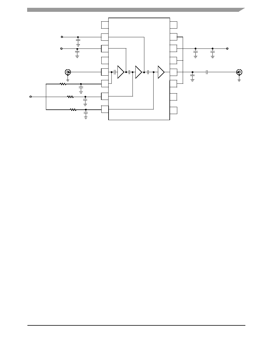
Figure 1. Functional Block Diagram
V
D1
V
D2
Figure 2. Pin Connections
16
15
14
13
12
11
10
1
2
3
4
5
6
7
8
(Top View)
9
N.C.
V
D2
V
D1
GND
RF
in
V
GATE1
V
GATE2
V
GATE3
N.C.
V
D3
/RF
out
V
D3
/RF
out
V
D3
/RF
out
V
D3
/RF
out
V
D3
/RF
out
N.C.
N.C.
V
GATE3
V
D3
RF
out
RF
in
V
GATE1
V
GATE2
Note: Exposed backside flag is source
terminal for transistors.
© Freescale Semiconductor, Inc., 2005. All rights reserved.
2
RF Device Data
Freescale Semiconductor
MHVIC910HR2
Table 3. ESD Protection Characteristics
Test Conditions
Class
Human Body Model
0 (Minimum)
Machine Model
M2 (Minimum)
Table 4. Moisture Sensitivity Level
Test Methodology
Rating
Package Peak Temperature
Unit
Per JESD 22-A113, IPC/JEDEC J-STD-020
3
240
°C
Table 5. Recommended Operating Ranges
Parameter
Symbol
Value
Unit
Drain Supply Voltage
V
DD
26
Vdc
3rd Stage Quiescent Current
I
DQ3
150
mA
2nd Stage Quiescent Current
I
DQ2
50
mA
1st Stage Quiescent Current
I
DQ1
25
mA
Table 6. Electrical Characteristics
(T
A
= 25°C matched to a 50 system, unless otherwise noted)
V
DD
= 26 V, V
GS
set for I
DQ3
= 150 mA, frequency range 921-960 MHz
Characteristic
Symbol
Min
Typ
Max
Unit
Frequency Range
f
RF
921
--
960
MHz
Output Power @ 1 dB Compression Point
P @ 1dB
39
40
--
dBm
Power Gain @ P1dB
G @ 1dB
38
39
--
dB
Power Added Efficiency @ 1 dB Compression Point
PAE @ 1dB
43
48
--
%
Input Return Loss @ P1dB
IRL @ 1dB
--
-15
-10
dB
Gain Flatness @ 40 dBm
Variation (T
C
= -30 to +85°C @ 40 dBm)
G
F
G
V
--
--
.5
5
--
--
dB
dB
Load Stability
(V
DS
= 24 V to 28 V, P
out
= P1dB Down to 0 dBm,
All Phase Angles)
VSWR
10:1
--
--
--
Ruggedness
(V
DS
= 26 V, P
out
= 42 dBm, Load VSWR = 10:1,
All Phase Angles)
No Damage After Test
NOTE - CAUTION - MOS devices are susceptible to damage from electrostatic charge. Reasonable precautions in handling and
packaging MOS devices should be observed.
MHVIC910HR2
3
RF Device Data
Freescale Semiconductor
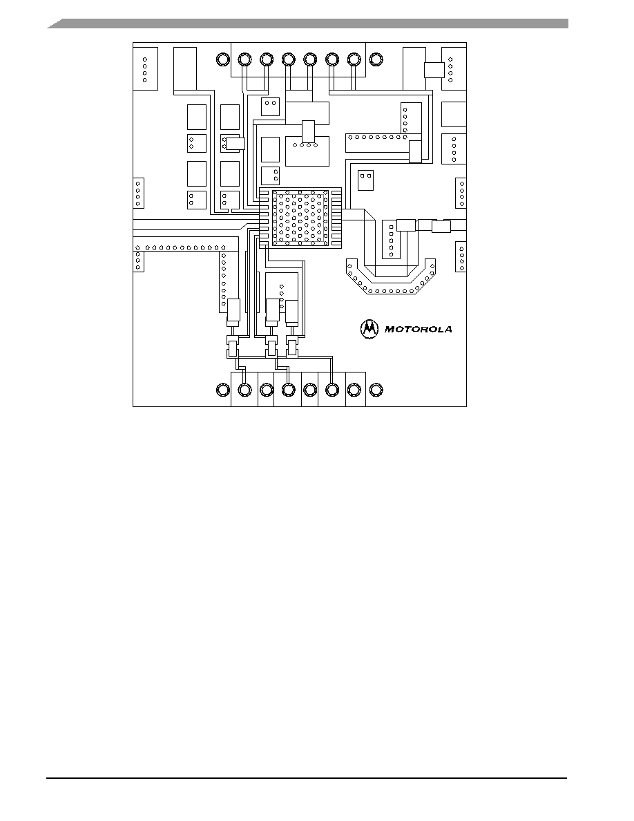
RF
OUTPUT
RF
INPUT
C1, C2, C3, C4, C5, C8
1
µF Surface Mount Chip Capacitors
C6
4.7 pF AVX Chip Capacitor, ACCU-P (08051J4R7BBT)
C7
47 pF AVX Chip Capacitor, ACCU-P (08055K470JBTTR)
C9
33 pF AVX Chip Capacitor, ACCU-P (08053J330JBT)
J1, J2
Header (Break-away), HDR2X10STIMCSAFU
J3, J4
SMA Connector 2052-1618-02 (Threaded)
R1, R2, R3
100
Chip Resistors (0402)
PCB
Rogers 04350, 20 mils
Figure 3. 921-960 MHz Demo Board Schematic
C9
V
D3
V
D1
V
D2
V
GS
C2
C3
C8
C6
C7
C4
C5
C1
R3
R1
R2
16
15
14
13
12
11
10
9
1
2
3
4
5
6
7
8
4
RF Device Data
Freescale Semiconductor
MHVIC910HR2
Figure 4. 921-960 MHz Demo Board Component Layout
V
G1
V
G2
V
G3
V
D1
V
D2
V
D3
C3
C2
C8
C7
C6
C9
C4
C5
C1
R3
R1
R2
RF Input
RF Output
900 MHz
MHVIC910HR2
Freescale has begun the transition of marking Printed Circuit Boards (PCBs) with the Freescale Semiconductor
signature/logo. PCBs may have either Motorola or Freescale markings during the transition period. These changes will have
no impact on form, fit or function of the current product.
MHVIC910HR2
5
RF Device Data
Freescale Semiconductor
TYPICAL CHARACTERISTICS
970
36
43
910
42
41
40
39
38
37
960
950
940
930
920
T
C
= -30
°C, I
DQ3
= 150 mA
T
C
= +25
°C, I
DQ3
= 150 mA
T
C
= +25
°C, I
DQ3
= 120 mA
T
C
= +25
°C, I
DQ3
= 110 mA
T
C
= +85
°C, I
DQ3
= 150 mA
100
5
1
10
3
-1
-3
-5
-7
-9
-11
-13
-15
1
I
DQ3
= 150 mA
f = 960 MHz
T
C
= -30
°C
+85
°C
+25
°C
970
36
43
910
42
41
40
39
38
37
960
950
940
930
920
T
C
= -30
°C, I
DQ3
= 150 mA
T
C
= +25
°C, I
DQ3
= 150 mA
T
C
= +25
°C, I
DQ3
= 120 mA
T
C
= +85
°C, I
DQ3
= 150 mA
43
12
35
0
T
C
= -30
°C, I
DQ3
= 150 mA
42
41
40
39
38
37
36
10
8
6
4
2
T
C
= +25
°C, I
DQ3
= 150 mA
T
C
= +25
°C, I
DQ3
= 120 mA
T
C
= +25
°C, I
DQ3
= 110 mA
T
C
= +85
°C, I
DQ3
= 150 mA
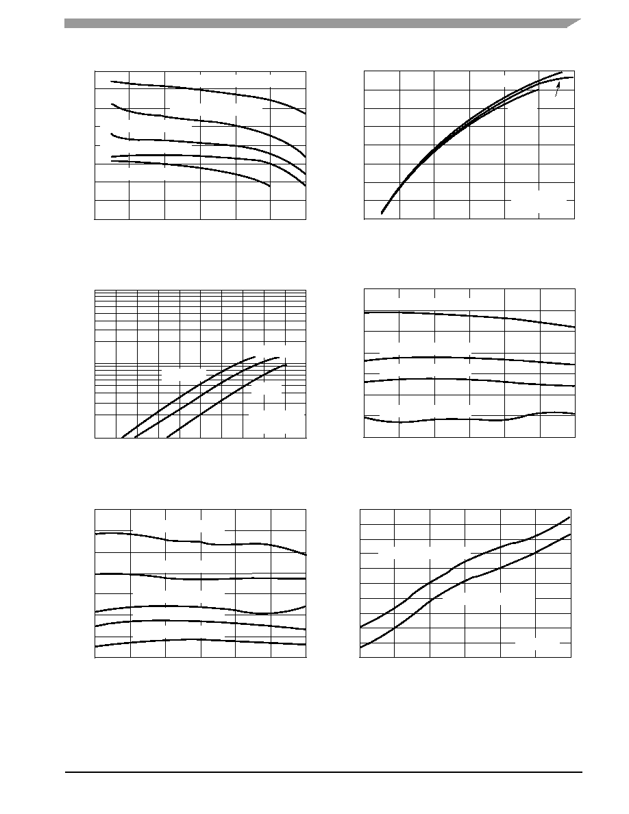
Figure 5. Power Gain versus
Output Power
P
out
, OUTPUT POWER (WATTS)
Figure 6. Power Added Efficiency
versus Output Power
P
out
, OUTPUT POWER (WATTS)
G
ps
, POWER GAIN (dB)
Figure 7. Output Power versus Input Power
Figure 8. Power Gain versus Frequency
P
out
= 10 W
f, FREQUENCY (MHz)
Figure 9. Power Gain versus Frequency
P
out
= P1dB
f, FREQUENCY (MHz)
P
AE, POWER
ADDED EFFICIENCY
(%)
G
,
POWER GAIN (dB)
ps
P
AE, POWER
ADDED EFFICIENCY
(%)
Figure 10. Power Added Efficiency versus Frequency
P
out
= 10 W
50
12
10
0
I
DQ3
= 150 mA
f = 960 MHz
T
C
= -30
°C
+85
°C
+25
°C
45
40
35
30
25
20
15
10
8
6
4
2
970
43
48
910
47.5
47
46.5
46
45.5
45
44.5
44
43.5
960
950
940
930
920
f = 960 MHz
T
C
= +25
°C, I
DQ3
= 150 mA
T
C
= +25
°C, I
DQ3
= 120 mA
P out
, OUTPUT
POWER (W
A
TTS)
P
in
, INPUT POWER (dBm)
G
,
POWER GAIN (dB)
ps
f, FREQUENCY (MHz)