MHV5IC2215NR2
1
RF Device Data
Freescale Semiconductor
RF LDMOS Wideband Integrated
Power Amplifier
The MHV5IC2215NR2 wideband integrated circuit is designed for base
station applications. It uses Freescale's High Voltage (28 Volts) LDMOS IC
technology and integrates a two - stage structure. Its wideband on - chip
matching design makes it usable from 1500 to 2200 MHz. The linearity
performances cover all modulation formats for cellular applications.
Driver Application
∑ Typical Single-Carrier N-CDMA Performance: V
DD
= 28 Volts, I
DQ1
=
164 mA, I
DQ2
= 115 mA, P
out
= 23 dBm, Full Frequency Band (1930-
1990 MHz), IS-95 CDMA (Pilot, Sync, Paging, Traffic Codes 8 Through
13) Channel Bandwidth = 1.2288 MHz. PAR = 9.8 dB @ 0.01%
Probability on CCDF.
Power Gain -- 27.5
dB
ACPR @ 885 kHz Offset -- -60 dBc in 30 kHz Bandwidth
∑ Typical Single-Carrier W-CDMA Performance: V
DD
= 28 Volts, I
DQ1
=
164 mA, I
DQ2
= 115 mA, P
out
= 23 dBm, Full Frequency Band (2130-
2170 MHz), Channel Bandwidth = 3.84 MHz, PAR = 8.5 dB @ 0.01%
Probability on CCDF.
Power Gain -- 24 dB
ACPR @ 5 MHz Offset -- -55 dBc in 3.84 MHz Channel Bandwidth
∑ Capable of Handling 3:1 VSWR, @ 28 Vdc, 2170 MHz, 15 Watts CW
Output Power
∑ Characterized with Series Equivalent Large-Signal Impedance Parameters
and Common Source Scattering Parameters
Features
∑ On-Chip Matching (50
Ohm Input, >5 Ohm Output)
∑ Integrated Quiescent Current Temperature Compensation
with Enable/Disable Function
∑ On-Chip Current Mirror g
m
Reference FET for Self Biasing Application
(1)
∑ Integrated ESD Protection
∑ RoHS Compliant
∑ In Tape and Reel. R2 Suffix = 1,500 Units per 16 mm, 13 inch Reel
1. Refer to AN1987, Quiescent Current Control for the RF Integrated Circuit Device Family. Go to http://www.freescale.com/rf.
Select Documentation/Application Notes - AN1987.
Document Number: MHV5IC2215N
Rev. 1, 5/2006
Freescale Semiconductor
Technical Data
MHV5IC2215NR2
CASE 978-03
PFP-16
2170 MHz, 23 dBm, 28 V
SINGLE N-CDMA, SINGLE W-CDMA
RF LDMOS WIDEBAND
INTEGRATED POWER AMPLIFIER
16
1
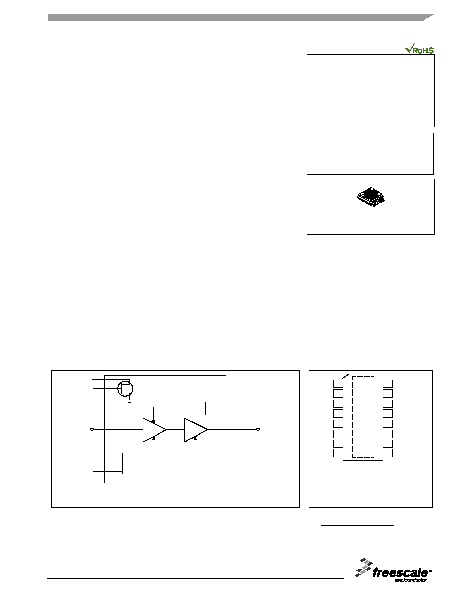
Note: Exposed backside flag is source
terminal for transistors.
16
15
14
13
12
11
10
1
2
3
4
5
6
7
8
(Top View)
9
N.C.
V
RD1
V
RG1
V
DS1
GND
V
GS1
V
GS2
N.C.
V
DS2
/RF
out
V
DS2
/RF
out
V
DS2
/RF
out
V
DS2
/RF
out
V
DS2
/RF
out
V
DS2
/RF
out
N.C.
RF
in
V
GS1
RF
in
V
DS1
V
GS2
V
DS2
/RF
out
2 Stage IC
Quiescent Current
Temperature Compensation
V
RD1
V
RG1
Figure 1. Block Diagram
Figure 2. Pin Connections
© Freescale Semiconductor, Inc., 2006. All rights reserved.

2
RF Device Data
Freescale Semiconductor
MHV5IC2215NR2
Table 1. Maximum Ratings
Rating
Symbol
Value
Unit
Drain-Source Voltage
V
DSS
-0.5, +65
Vdc
Gate-Source Voltage
V
GS
-0.5, +12
Vdc
Storage Temperature Range
T
stg
- 65 to +150
∞C
Operating Junction Temperature
T
J
150
∞C
Input Power
P
in
12
dBm
Table 2. Thermal Characteristics
Characteristic
Symbol
Value
(1)
Unit
Thermal Resistance, Junction to Case
Driver Application
Stage 1, 28 Vdc, I
DQ1
= 164 mA
(P
out
= 23 dBm CW)
Stage 2, 28 Vdc, I
DQ2
= 115 mA
R
JC
9.3
3.5
∞C/W
Table 3. ESD Protection Characteristics
Test Methodology
Class
Human Body Model (per JESD22-A114)
0 (Minimum)
Machine Model (per EIA/JESD22-A115)
A (Minimum)
Charge Device Model (per JESD22-C101)
III (Minimum)
Table 4. Moisture Sensitivity Level
Test Methodology
Rating
Package Peak Temperature
Unit
Per JESD 22-A113, IPC/JEDEC J-STD-020
3
260
∞C
Table 5. Electrical Characteristics
(T
C
= 25∞C unless otherwise noted)
Characteristic
Symbol
Min
Typ
Max
Unit
W-CDMA Functional Tests (In Freescale Test Fixture, 50 ohm system) V
DD
= 28 Vdc, I
DQ1
= 164 mA, I
DQ2
= 115 mA, P
out
= 23 dBm,
f = 2140 MHz, Single-carrier W-CDMA, 3.84 MHz Channel Bandwidth Carrier. ACPR measured in 3.84 MHz Channel Bandwidth @ ±5 MHz
Offset. PAR = 8.5 dB @ 0.01% Probability on CCDF.
Power Gain
G
ps
23
24
27
dB
Gain Flatness in 60 MHz Bandwidth @ P
out
= 23 dBm
f = 2110-2170 MHz
G
F
--
0.3
0.5
dB
Adjacent Channel Power Ratio
ACPR
--
-56
-54
dBc
Input Return Loss
IRL
--
-12
-10
dB
Typical N-CDMA Tests (In Freescale Test Fixture, 50 ohm system) V
DD
=
28 Vdc, I
DQ1
= 164 mA, I
DQ2
= 115 mA, P
out
= 23 dBm,
f = 1960
MHz, Single-Carrier N-CDMA, 1.2288 MHz Channel Bandwidth Carrier. ACPR measured in 30 kHz Channel Bandwidth
@ ±885 kHz Offset. PAR = 9.8 dB @ 0.01% Probability on CCDF
Power Gain
G
ps
25.5
27.5
29
dB
Gain Flatness @ P
out
= 23 dBm
f = 1930-1990 MHz
G
F
--
0.3
--
dB
Adjacent Channel Power Ratio
ACPR
--
-60
--
dBc
Input Return Loss
IRL
--
-12
--
dB
Deviation from Linear Phase in 60 MHz Bandwidth
@ P
out
= 23 dBm
--
0.2
--
∞
Delay @ P
out
= 23 dBm Including Output Matching
Delay
--
1.5
--
ns
1. Refer to AN1955, Thermal Measurement Methodology of RF Power Amplifiers. Go to http://www.freescale.com/rf.
Select Documentation/Application Notes - AN1955.

MHV5IC2215NR2
3
RF Device Data
Freescale Semiconductor
W-CDMA DRIVER APPLICATION
Figure 3. MHV5IC2215NR2
Test Circuit Schematic
RF
OUTPUT
RF
INPUT
Z12
Z1
Z2
Z3
Z4
C1
V
GS2
R2
C3
V
GS1
R1
+
C5
C4
+
C2
C8
Z11
C7
+
+
C6
Z5
Z6
Z7
Z8
Z9
C11
C10
Z10
C9
NC
NC
V
DS2
V
DS1
V
RG1
V
RD1
NC
Quiescent Current
Temperature Compensation
1
2
3
4
5
6
7
8
16
15
14
13
12
11
10
9
Z8
0.0105 x 0.1200 Microstrip
Z9
0.0559 x 0.1145 Microstrip
Z10
0.045 x 0.2671 Microstrip
Z11
0.0349 x 0.3319 Microstrip
Z12
0.0027 x 2.0413 Microstrip
Z13
0.0349 x 0.9151 Microstrip
PCB
Rogers 4350, 0.020,
r
= 3.5
Z1
0.045 x 0.1289 Microstrip
Z2
0.0443 x 0.0161 Microstrip
Z3
0.0308 x 0.0416 x 0.03 Taper
Z4
0.0161 x 0.0685 Microstrip
Z5
0.0838 x 0.1759 Microstrip
Z6
0.0503 x 0.1759 Microstrip
Z7
0.0922 x 0.1759 Microstrip
Z13
Table 6. MHV5IC2215NR2
Test Circuit Component Designations and Values
Part
Description
Part Number
Manufacturer
C1
22 pF, 50 V Chip Capacitor (0603)
06033J220GBT
AVX
C2, C3
6.8 pF, 50 V Chip Capacitors (0603)
06035J6R8BBT
AVX
C4, C7
1 F, 35 V Tantalum Chip Capacitors
TAJA105K035R
Kemet
C5, C6
330 F, 50 V Electrolytic Chip Capacitors
MCR35V337M10X16
Multicomp
C8
0.01 F, 50 V Chip Capacitor (0805)
0805C103K5RACTR
Vishay
C9, C10
2.7 pF, 50 V Chip Capacitors (0603)
06035J2R7BBT
AVX
C11
15 pF, 25 V Chip Capacitor (0603)
06033J150GBT
AVX
R1, R2
1 kW Chip Resistors
P1.00KCCT-ND
Panasonic

4
RF Device Data
Freescale Semiconductor
MHV5IC2215NR2
W-CDMA DRIVER APPLICATION
Figure 4. MHV5IC2215NR2 Test Circuit Component Layout
C9
C10
C11
C8
C7
C5
C6
C4
V
D1
V
D2
C1
C3
C2
R1
R2
V
G1
V
G2
MHV5IC2215, Rev. 1
MHV5IC2215NR2
5
RF Device Data
Freescale Semiconductor
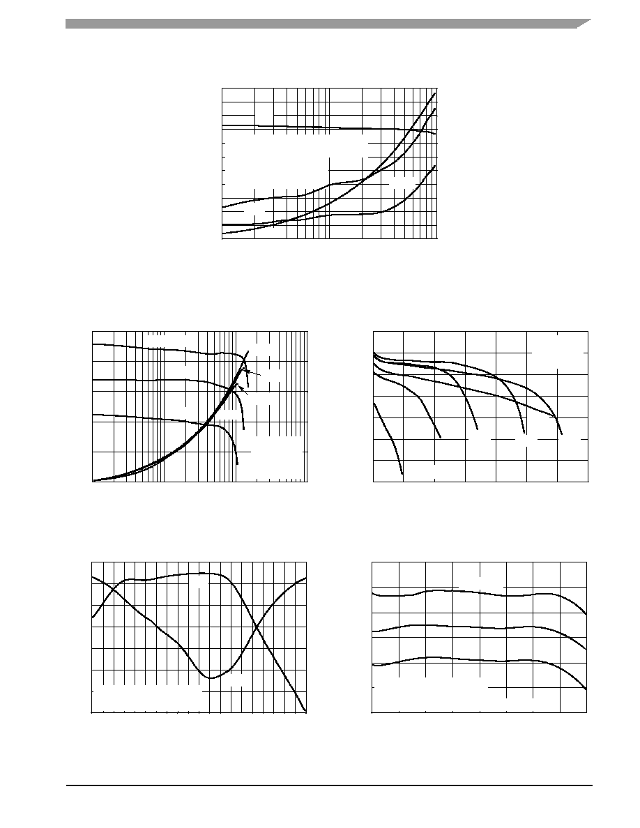
TYPICAL W-CDMA DRIVER APPLICATION CHARACTERISTICS
IM3
(dBc), ACPR (dBc)
0
-66
P
out
, OUTPUT POWER (WATTS) AVG.
33
0
27
-12
21
-24
15
-36
3
-60
0.1
1
10
PAE
G
ps
ACPR
IM3
-48
9
Figure 5. 2-Carrier W-CDMA ACPR, IM3, Power
Gain and Power Added Efficiency
versus Output Power
PA
E
, POWER ADDED EFFICIENCY (%), G
ps
, POWER GAIN (dB)
30
24
18
12
6
-6
-18
-30
-42
-54
V
DD
= 28 Vdc, I
DQ1
= 164 mA, I
DQ2
= 115 mA
f1 = 2135 MHz, f2 = 2145 MHz, 2 x W-CDMA
10 MHz in 3.84 MHz Bandwidth
PAR = 8.5 dB @ 0.01%
Probability (CCDF)
100
18
28
0.1
0
50
V
DD
= 28 Vdc
I
DQ1
= 164 mA
I
DQ2
= 115 mA
f = 2140 MHz
T
C
= -30
_C
-30
_C
25
_C
85
_C
10
1
26
24
22
20
40
30
20
10
P
out
, OUTPUT POWER (WATTS) CW
Figure 6. Power Gain and Power Added
Efficiency versus Output Power
G
ps
, POWER GAIN (dB)
P
AE, POWER ADDED EFFICIENCY (%)
PAE
G
ps
25
_C
85
_C
P
out
, OUTPUT POWER (WATTS) CW
Figure 7. Power Gain versus Output Power
I
DQ1
= 164 mA
I
DQ2
= 115 mA
f = 2140 MHz
V
DD
= 12 V
32 V
10
19
26
0
8
25
24
23
20
22
21
2
4
6
G
ps
, POWER GAIN (dB)
12
14
28 V
24 V
20 V
16 V
3000
-21
28
1000
-16
-2
S21
f, FREQUENCY (MHz)
Figure 8. Broadband Frequency Response
S11
21
-4
14
-6
7
-8
0
-10
-7
-12
-14
-14
2500
2000
1500
V
DD
= 28 Vdc, P
out
= 23 dBm CW
I
DQ1
= 164 mA, I
DQ2
= 115 mA
S1
1 (dB)
S21 (dB)
2300
18
30
1900
T
C
= -30
_C
25
_C
85
_C
26
24
22
20
1950
2050
2150
f, FREQUENCY (MHz)
Figure 9. Power Gain versus Frequency
G
ps
, POWER GAIN (dB)
28
2000
2100
2200
2250
V
DD
= 28 Vdc, P
out
= 23 dBm CW
I
DQ1
= 164 mA, I
DQ2
= 115 mA
Two-Tone Measurements, Center Frequency = 2140 MHz