 | –≠–ª–µ–∫—Ç—Ä–æ–Ω–Ω—ã–π –∫–æ–º–ø–æ–Ω–µ–Ω—Ç: MC33199 | –°–∫–∞—á–∞—Ç—å:  PDF PDF  ZIP ZIP |

10
MC33199
SEMICONDUCTOR
TECHNICAL DATA
ISO 9141
SERIAL LINK DRIVER
Order this document by MC33199/D
D SUFFIX
PLASTIC PACKAGE
CASE 751A
(SO≠14)
14
1
Device
Operating
Temperature Range
Package
ORDERING INFORMATION
MC33199D
TA = ≠ 40
∞
to +125
∞
C
SO≠14
PIN CONNECTIONS
1
14
13
12
11
9
8
2
3
4
5
6
7
(Top View)
VCC
REF≠IN≠L
REF≠IN≠K
TXD
NC
REF≠OUT
LO
RXD
VS
L
I1
Gnd
DIA
NC
1
MOTOROLA ANALOG IC DEVICE DATA
Automotive ISO 9141
Serial Link Driver
The MC33199D is a serial interface circuit used in diagnostic
applications. It is the interface between the microcontroller and the special
K and L Lines of the ISO diagnostic port. The MC33199D has been
designed to meet the "Diagnosis System ISO 9141" specification.
The device has a bi≠directional bus K Line driver, fully protected against
short circuits and over temperature. It also includes the L Line receiver,
used during the wake up sequence in the ISO transmission.
The MC33199 has a unique feature which allows transmission baud rate
up to 200 k baud.
∑
Electrically Compatible with Specification "Diagnosis System ISO 9141"
∑
Transmission Speed Up to 200 k Baud
∑
Internal Voltage Reference Generator for Line Comparator Thresholds
∑
TXD, RXD and LO Pins are 5.0 V CMOS Compatible
∑
High Current Capability of DIA Pin (K Line)
∑
Short Circuit Protection for the K Line Input
∑
Over Temperature Shutdown with Hysteresis
∑
Large Operating Range of Driver Supply Voltage
∑
Full Operating Temperature Range
∑
ESD Protected Pins
+
≠
+
≠
C2
Thermal
Shutdown
Simplified Application
REF≠OUT
LO
REF≠IN≠L
REF≠IN≠K
RXD
TXD
VCC
L
I1
DIA
Gnd
VS
I1
Source
Reference
Generator
Protection
Current
Limit
VCC
Driver
C1
This device contains 94 active transistors.
©
Motorola, Inc. 1996
Rev 0

MC33199
2
MOTOROLA ANALOG IC DEVICE DATA
MAXIMUM RATINGS
(Note 1)
Rating
Symbol
Value
Unit
VS Supply Pin
DC Voltage Range
Transient Pulse (Note 2)
VS
Vpulse
≠0.5 to +40
≠2.0 to +40
V
VCC Supply DC Voltage Range
VCC
≠0.3 to +6.0
V
DIA and L Pins (Note 2)
DC Voltage Range
Transient Pulse (Clamped by Internal Diode)
DC Source Current
DIA Low Level Sink Current
≠
≠0.5 to +40
≠2.0
≠50
Int. Limit
V
V
mA
mA
TXD DC Voltage Range
≠
≠0.3 to
VCC + 0.3
V
REF≠IN DC Voltage Range
VS < VCC
VS > VCC
≠
≠0.3 to VCC
≠0.3 to VS
V
ESD Voltage Capability (Note 3)
V(ESD)
±
2000
V
NOTES: 1. The device is compatible with Specification: "Diagnosis System ISO 9141".
2. See the test circuit (Figure 23). Transient test pulse according to ISO 76371 and DIN 40839;
highest test levels.
3. Human Body Model; C = 100 pF, R = 1500
.
THERMAL RATINGS
Rating
Symbol
Value
Unit
Storage Temperature
Tstg
≠55 to +150
∞
C
Operating Junction Temperature
TJ
≠40 to +150
∞
C
Thermal Resistance, Junction≠to≠Ambient
R
JA
180
∞
C/W
Maximum Power Dissipation (@ TA = 105
∞
C)
PD
250
mW
ELECTRICAL CHARACTERISTICS
(≠ 40
∞
C
TA
125
∞
C, 4.5 V
VCC
5.5 V, 4.5 V
VS
20 V, unless otherwise
noted. Typical values reflect approximate mean at 25
∞
C, nominal VCC and VS, at time of device characterization.)
Characteristic
Symbol
Min
Typ
Max
Unit
VCC PIN 1
VCC Supply Voltage Range
VCC
4.5
≠
5.5
V
VCC Supply Current (Note 1)
ICC
0.5
1.0
1.5
mA
REF≠IN≠L PIN 2 AND REF≠IN≠K PIN 3
REF≠IN≠L and REF≠IN≠K Input Voltage Range
For 0 < VS < VCC
For VCC < VS < 40 V
Vinref
2.0
2.0
≠
≠
VCC ≠ 2.0 V
VS ≠ 1.0 V
V
REF≠IN≠L and REF≠IN≠K Inputs Currents
IVIN
≠5.0
≠
5.0
µ
A
LO PIN 4
LO Open Collector Output
Low Level Voltage @ Iout = 1.0 mA
Low Level Voltage @ Iout = 4.0 mA
VOL
≠
≠
0.34
≠
0.7
0.8
V
RXD PIN 5
Pull≠Up Resistor to VCC
RRXD
1.5
2.0
2.5
k
Low Level Voltage @ Iout = 1.0 mA
VOL
≠
0.3
0.7
V
NOTES: 1. Measured with TXD = VCC, I1 = VS, DIA and L high, no load. REF≠IN≠L and REF≠IN≠K connected to REF≠OUT.
2. 0 < VCC < 5.5 V, 0 < VS < 40 V, 0 < VDIA < 20 V, TXD high or floating.
3. When an over temperature is detected, the DIA output is forced "off".
4. 0 < VCC < 5.5 V, 0 < VS < 40 V, 0 < VL < 20 V.
5. At static "High" or "Low" level TXD, the current source I1 delivers a current of 3.0 mA (typ). Only during "Low" to "High" transition, does this current
increase to a higher value in order to charge the K Line capacitor (CL < 4.0 nF) in a short time (see Figure 3).
6. Measured with TXD = VCC, I1 = VS, DIA and L high, no load, REF≠IN≠L and REF≠IN≠K connected to REF≠OUT.

MC33199
3
MOTOROLA ANALOG IC DEVICE DATA
ELECTRICAL CHARACTERISTICS (continued)
(≠ 40
∞
C
TA
125
∞
C, 4.5 V
VCC
5.5 V, 4.5 V
VS
20 V, unless otherwise
noted. Typical values reflect approximate mean at 25
∞
C, nominal VCC and VS, at time of device characterization.)
Characteristic
Unit
Max
Typ
Min
Symbol
TXD PIN 6
High Level Input Voltage
VIH
0.7 VCC
2.8
≠
V
Low Level Input Voltage
VIL
≠
2.0
0.3 VCC
V
Input Current @ 0 < VS < 40 V
TXD at High Level
TXD at Low Level
IH
IL
≠200
≠600
≠
≠
30
≠100
µ
A
DIA INPUT/OUTPUT PIN 9
Low Level Output Voltage @ I = 30 mA
VOL
0
0.35
0.8
V
Drive Current Limit
ILim
40
≠
120
mA
High Level Input Threshold Voltage
(REF≠IN≠K Connected to REF≠OUT)
VIH
Vref min
+ 0.25 V
Vref
+ 0.325 V
Vref max
+ 0.4 V
V
Low Level Input Threshold Voltage
(REF≠IN≠K Connected to REF≠OUT)
VIL
Vref min
≠ 0.2 V
Vref
≠ 0.125 V
Vref max
≠ 0.05 V
V
Input Hysteresis
VHyst
300
450
600
mV
Positive Clamp @ 5.0 mA
VCl+
37
40
44
V
Negative Clamp @ ≠ 5.0 mA
VCl≠
≠1.5
≠0.6
≠0.3
V
Leakage Current (Note 2)
ILeak
4.0
10
16
µ
A
Over Temperature Shutdown (Note 3)
TLim
155
≠
≠
∞
C
L INPUT PIN 12
High Level Input Threshold Voltage
(REF≠IN≠L Connected to REF≠OUT)
VIH
Vref min
+ 0.25 V
Vref
+ 0.325 V
Vref max
+ 0.4 V
V
Low Level Input Threshold Voltage
(REF≠IN≠L Connected to REF≠OUT)
VIL
Vref min
≠ 0.2 V
Vref
≠ 0.125 V
Vref max
≠ 0.05 V
V
Input Hysteresis
VHyst
300
450
600
mV
Leakage Current (Note 4)
ILeak
4.0
10
16
µ
A
Positive Clamp @ 5.0 mA
VCl+
37
40
44
V
Negative Clamp @ ≠ 5.0 mA
VCl≠
≠1.5
≠0.6
≠0.3
V
I1 PIN 11
Static Source Current
I1s
≠4.0
≠3.0
≠2.0
mA
Static Saturation Voltage (I1s = ≠ 2.0 mA)
VI1(sat)
VS ≠ 1.2
VS ≠ 0.8
VS
V
Dynamic Source Current (Note 5)
I1d
≠120
≠80
≠40
mA
Dynamic Saturation Voltage (II1(sat) = ≠ 40 mA)
VI1(dsat)
VS ≠ 2.7
VS ≠ 0.85
VS
V
VS PIN 13
VS Supply Voltage Range
VS
4.5
≠
20
V
VS Supply Current (Note 6)
IS
0.5
1.3
2.0
mA
NOTES: 1. Measured with TXD = VCC, I1 = VS, DIA and L high, no load. REF≠IN≠L and REF≠IN≠K connected to REF≠OUT.
2. 0 < VCC < 5.5 V, 0 < VS < 40 V, 0 < VDIA < 20 V, TXD high or floating.
3. When an over temperature is detected, the DIA output is forced "off".
4. 0 < VCC < 5.5 V, 0 < VS < 40 V, 0 < VL < 20 V.
5. At static "High" or "Low" level TXD, the current source I1 delivers a current of 3.0 mA (typ). Only during "Low" to "High" transition, does this current
increase to a higher value in order to charge the K Line capacitor (CL < 4.0 nF) in a short time (see Figure 3).
6. Measured with TXD = VCC, I1 = VS, DIA and L high, no load, REF≠IN≠L and REF≠IN≠K connected to REF≠OUT.

MC33199
4
MOTOROLA ANALOG IC DEVICE DATA
ELECTRICAL CHARACTERISTICS (continued)
(≠ 40
∞
C
TA
125
∞
C, 4.5 V
VCC
5.5 V, 4.5 V
VS
20 V, unless otherwise
noted. Typical values reflect approximate mean at 25
∞
C, nominal VCC and VS, at time of device characterization.)
Characteristic
Unit
Max
Typ
Min
Symbol
REF≠OUT PIN 14
Output Voltage
3.0 < VS < 5.6 V and IRO =
±
10
µ
A
5.6 < VS < 18 V and IRO =
±
10
µ
A
18 < VS < 40 V and IRO =
±
10
µ
A
Vref
2.7
0.5 x VS
8.5
≠
≠
≠
3.3
0.56 x VS
10.8
V
Maximum Output Current
Iout
≠50
≠
50
µ
A
Pull≠Up Resistor to VCC
RPU
3.0
8.0
12
k
NOTES: 1. Measured with TXD = VCC, I1 = VS, DIA and L high, no load. REF≠IN≠L and REF≠IN≠K connected to REF≠OUT.
2. 0 < VCC < 5.5 V, 0 < VS < 40 V, 0 < VDIA < 20 V, TXD high or floating.
3. When an over temperature is detected, the DIA output is forced "off".
4. 0 < VCC < 5.5 V, 0 < VS < 40 V, 0 < VL < 20 V.
5. At static "High" or "Low" level TXD, the current source I1 delivers a current of 3.0 mA (typ). Only during "Low" to "High" transition, does this current
increase to a higher value in order to charge the K Line capacitor (CL < 4.0 nF) in a short time (see Figure 3).
6. Measured with TXD = VCC, I1 = VS, DIA and L high, no load, REF≠IN≠L and REF≠IN≠K connected to REF≠OUT.
DYNAMIC CHARACTERISTICS
(≠ 40
∞
C
TA
125
∞
C, 4.5 V
VCC
5.5 V, 4.5 V
VS
20 V, unless otherwise noted.)
Characteristic
Symbol
Min
Typ
Max
Unit
Transmission Speed
1/t Bit
0
≠
200 k
Baud
High or Low Bit Time
t Bit
5.0
≠
≠
µ
s
RXD Output
Low to High Transition Delay Time
High to Low Transition Delay Time
tRDR
tRDF
≠
≠
≠
≠
450
450
ns
LO Output
Low to High Transition Delay Time
High to Low Transition Delay Time
tLDR
tLDF
≠
≠
≠
≠
2.0
2.0
µ
s
DIA Output
Low to High Transition Delay Time
High to Low Transition Delay Time
tDDR
tDDF
≠
≠
≠
≠
650
650
ns
I1 Output (VS ≠ I1 > 2.7 V)
Rise Time
Hold Time
tI1R
tI1F
≠
1.5
≠
≠
0.3
4.5
µ
s
MC33199
5
MOTOROLA ANALOG IC DEVICE DATA
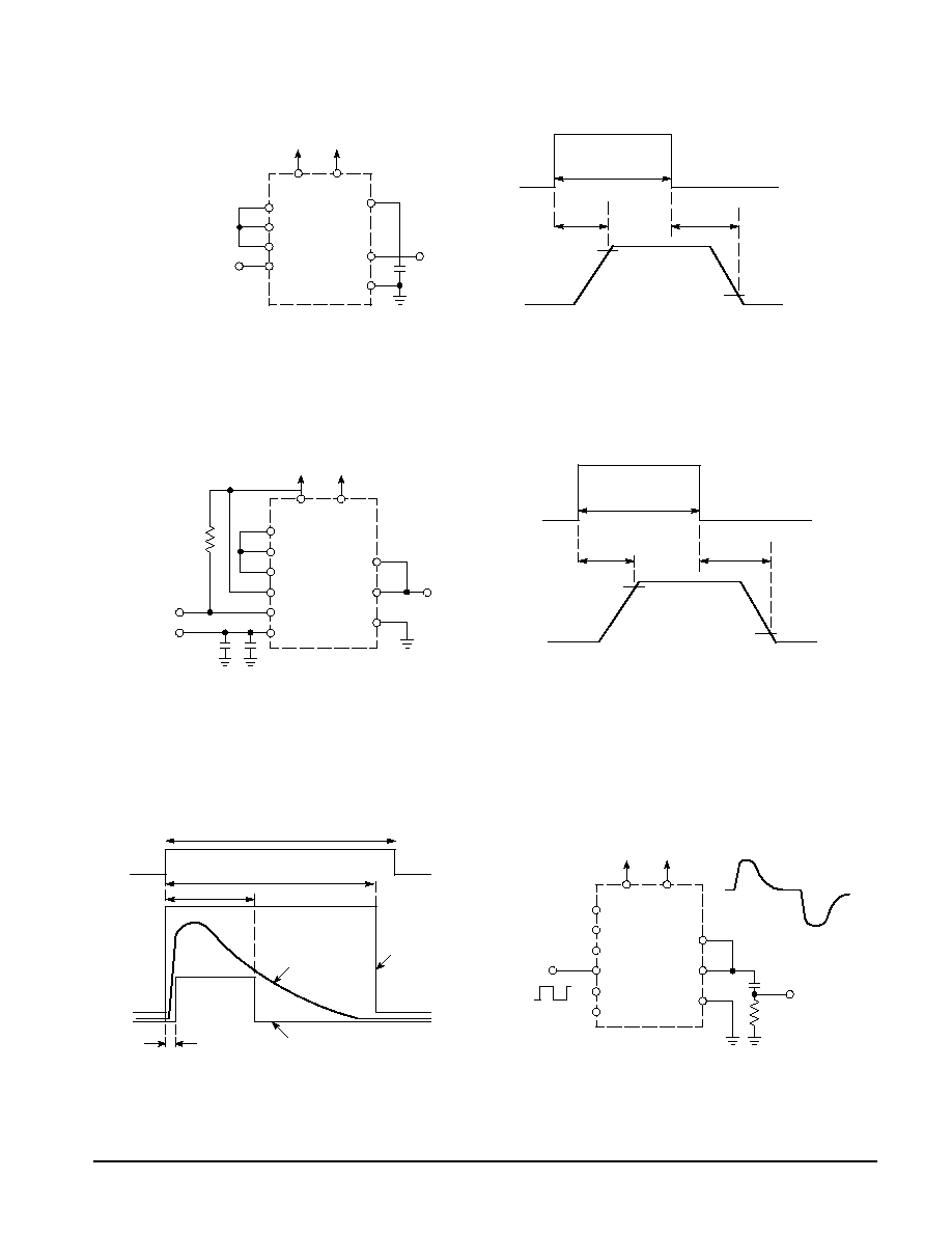
Figure 1. TXD to DIA AC Characteristic
+ 5.0 V
REF≠OUT
Input
Signal
REF≠IN≠L
REF≠IN≠K
TXD
1.0 nF
+12 V
VCC
Vbat
Test
Point
5.0 V
0 V
tBit
TXD Input
Signal
tDDF
tDDR
10 V
DIA Output
Signal
2.0 V
I1
DIA
Gnd
REF≠OUT
REF≠IN≠L
REF≠IN≠K
TXD
LO
RXD
+ 5.0 V +12 V
2.0 K
Test
Points
2 x 30 pF
VCC
Vbat
L
DIA
Gnd
Input
Signal
tBit
4.5 V
RXD to LO
Output Signal
0.4 V
12 V
0 V
DIA and L
Input Signal
tRDF/tLDF
tRDR/tLDR
Figure 2. DIA to TXD and L to LO AC Characteristics
tBit
tI1F
tI1H
TXD
Signal
5.0 V
0 V
Current Source
I1 Maximum Limit
Typical I1
Waveform
Current Source
I1 Minimum Limit
tI1R
120 mA
40 mA
4.0 mA
2.0 mA
Figure 3. Current Source I1 AC Characteristics
At static "High" or "Low" level TXD, the current source I1 delivers a
current of 3.0 mA (typ). Only during "Low" to "High" transition, does this
current increase to a higher value in order to charge the K Line
capacitor (Cl < 4.0 nF) in a short time.
REF≠OUT
REF≠IN≠L
REF≠IN≠K
TXD
LO
RXD
+ 5.0 V
+12 V
VCC
Vbat
I1
DIA
Gnd
Input
Signal
To
Oscilloscope
10
33 nF
I1 Pulse
Current
DIA Discharge
Current
Figure 4. Current Source I1 and DIA Discharge
Current Test Schematic