 | –≠–ª–µ–∫—Ç—Ä–æ–Ω–Ω—ã–π –∫–æ–º–ø–æ–Ω–µ–Ω—Ç: M51971 | –°–∫–∞—á–∞—Ç—å:  PDF PDF  ZIP ZIP |

MOTOR SPEED CONTROL
M51971L/FP
MITSUBISHI <CONTROL / DRIVER IC>
9
10
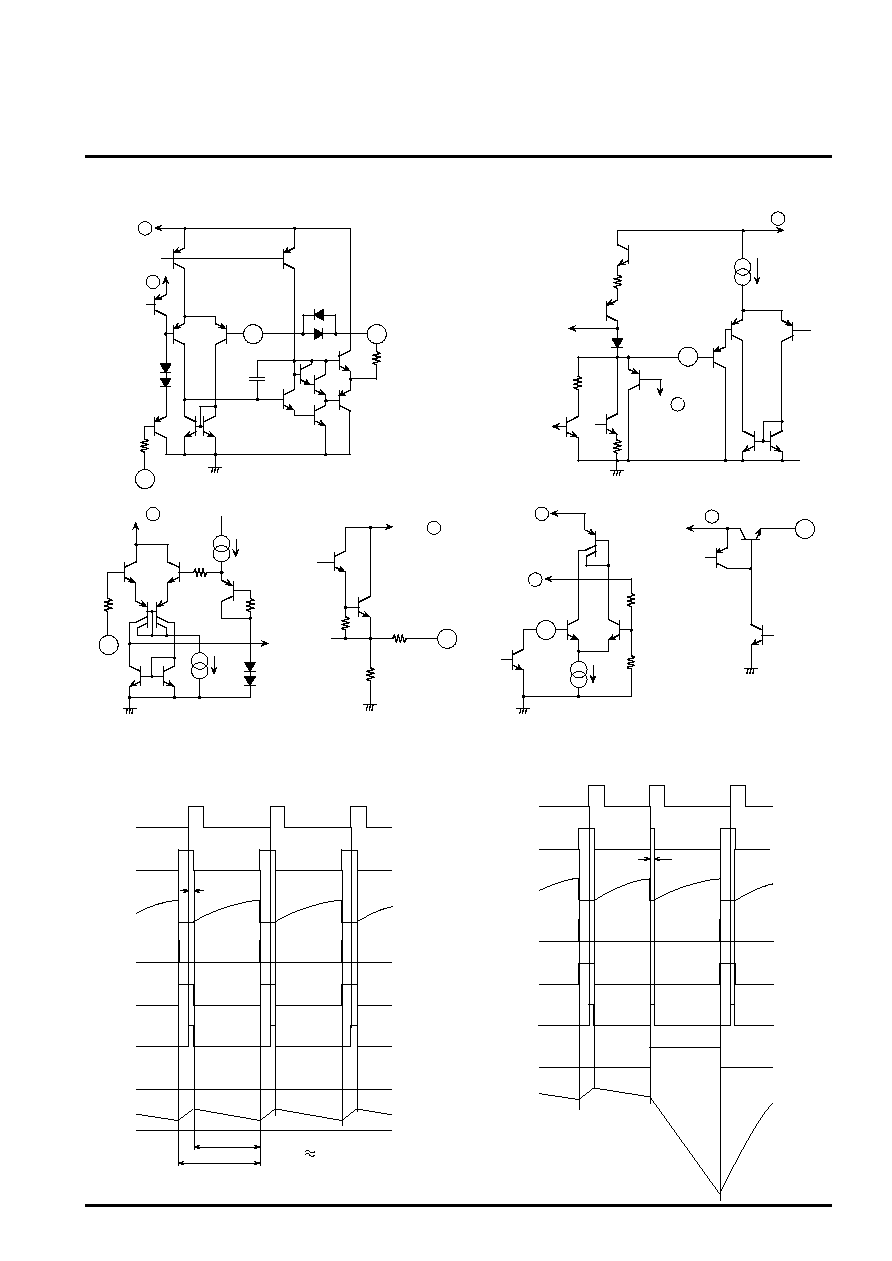
PIN CONFIGURATION (TOP VIEW)
DESCRIPTION
The M51971 is a semiconductor integrated circuit designed to
control the motor rotating speed.
The built-in FG amplifier with high gain enables to use a wide
range of rotating speed detector (FG detector).
Use of less external parts enables DC motors to be controlled with
high precision.
FEATURES
q
Wide range of supply voltage
∑ ∑ ∑ ∑ ∑ ∑ ∑ ∑ ∑ ∑ ∑ ∑ ∑ ∑ ∑ ∑ ∑ ∑ ∑ ∑ ∑ ∑ ∑ ∑ ∑ ∑ ∑ ∑ ∑
4 ≠ 17.5V
q
Variation coefficient of supply voltage
∑ ∑ ∑ ∑ ∑
±
0.005%/V (standard)
q
Load variation coefficient
∑ ∑ ∑ ∑ ∑
±
0.01% (standard, full load range)
q
Temperature coefficient of rotating speed
∑ ∑ ∑ ∑
7ppm/∞C (standard)
q
Built-in high performance FG amplifier
APPLICATION
Motor rotating speed control in floppy disk driver, player, tape
recorder, car stereo, etc.
RECOMMENDED OPERATING CONDITIONS
Supply voltage range
∑ ∑ ∑ ∑ ∑ ∑ ∑ ∑ ∑ ∑ ∑ ∑ ∑ ∑ ∑ ∑ ∑ ∑ ∑ ∑ ∑ ∑ ∑ ∑ ∑ ∑ ∑ ∑ ∑ ∑ ∑ ∑ ∑ ∑ ∑ ∑
4 ≠ 17.5V
Rated supply voltage
∑ ∑ ∑ ∑ ∑ ∑ ∑ ∑ ∑ ∑ ∑ ∑ ∑ ∑ ∑ ∑ ∑ ∑ ∑ ∑ ∑ ∑ ∑ ∑ ∑ ∑ ∑ ∑ ∑ ∑ ∑ ∑ ∑ ∑ ∑ ∑ ∑ ∑ ∑ ∑ ∑ ∑ ∑ ∑
9V
Input voltage range at pin
∑ ∑ ∑ ∑ ∑ ∑ ∑ ∑ ∑ ∑ ∑ ∑ ∑ ∑ ∑ ∑ ∑
-0.4 ≠ Vcc Note 1
Input voltage range at pin
∑ ∑ ∑ ∑ ∑ ∑ ∑ ∑ ∑ ∑ ∑ ∑ ∑ ∑ ∑ ∑ ∑ ∑ ∑ ∑ ∑ ∑ ∑ ∑ ∑ ∑
-0.4 ≠ Vcc
Highest setup tacho-generator frequency
∑ ∑ ∑ ∑ ∑ ∑ ∑ ∑ ∑ ∑ ∑ ∑ ∑ ∑ ∑ ∑
2.5kHz
Minimum trigger pulse width (input pulse at pin
)
∑ ∑ ∑ ∑ ∑ ∑ ∑ ∑ ∑ ∑
40
µ
s Note 2
Note 1: The linear operation range is -0.4 to +0.4V.
Note 2: This condition applies to both periods: from pulse rising to
pulse falling and pulse falling to pulse rising.
Outline 10P5
1
4
3
2
5
6
7
8
Schmitt input
Non-inverted input
Inverted input
Amplifier output
Time constant
Stabilized voltage
M5
1971L
GND
Integration capacitance
BLOCK DIAGRAM
1
4
4
Output
Power supply
10
7
8
9
1
4
3
2
6
5
Outline 10P2-C
M5
1971F
P
Non-inverted input
Inverted input
Amplifier output
Schmitt input
Time constant
Power supply
Output
Integration capacitance
GND
Stabilized voltage
1
2
10
7
6
Non-inverted input
Inverted input
Power supply
Operational
amplifier
V
LS
1.9V
Amplifier
output
Schmitt
intput
Stabilized supply
voltage
3
4
Schmitt
comparator
5
Time constant
Integration
capacitance
8
V
LS
1.9V
9
Over-shoot
prevention
circuit
Timer
Constant
current
control
Buffer
amplifier
Output
GND
Stabilized
voltage
MOTOR SPEED CONTROL
M51971L/FP
MITSUBISHI <CONTROL / DRIVER IC>
Voltage at pin
37
Supply voltage
Apply voltage at pin
1
Source current at pin
3
V
mA
V
V
Vcc
ABSOLUTE MAXIMUM RATINGS (Ta=25
∞
C unless otherwise noted)
Symbol
Ratings
Unit
Parameter
Conditions
V
18
-3
≠
Vcc
-5
0
≠
Vcc
880 (M51971L)
mW /
∞
C
mW
mA
mA
V
ELECTRICAL CHARACTERISTICS (Ta=25
∞
C, Vcc=9V unless otherwise noted)
Limits
Min.
Typ.
Max.
Symbol
Test conditions
Unit
Parameter
V
CC
Supply voltage range
4.0
Circuit current
6.0
2.44
I
CC
V
S
I
2.27
Stabilized supply voltage
Pd
F
Power dissipation
Topr
Tstg
Thermal derating
1
450 (M51971FP)
∞
C
V
LS
A
V
FG amplifier voltage gain
1
1
-3.0
-180
1.51
54
2.71
3.2
-0.5
-30
1.89
59
0.4
16
17.5
2.98
64
nA
dB
I
3
I
6
V
4
I
9
K
F
Source current at pin
6
Apply voltage at pin
4
Source current at pin
9
Operating temperature
Storage temperature
Ta
25∞C
-5
-20
8.8 (M51971L)
4.5 (M51971FP)
-20
≠
+75
-40
≠
+125
V
V
mA
∞
C
r
CD
T
R
= 75k
One-shot pulse width
Buffer amplifier offset voltage
V
BO
I
2
I
4
V
TH
4
V
HY
4
V
S
5
I
C
8
R
9
V
max
9
V
min
9
Input current at pin
1
Input current at pin
2
Level shift voltage at pin
1
Input current at pin
4
Threshold voltage at pin
4
Hysteresis width at pin
4
Saturation voltage at pin
5
Charging current at pin
8
Ratio of charging to discharging current at pin
8
Output protection resistance at pin
9
Maximum voltage at pin
9
Minimum voltage at pin
9
6
V =
0V
1
V =
0V
1
V =
0V
1
V =0.2mVrms, f=500Hz,
External set gain=60dB
1
V =
2.5V
4
Uses level shift voltage at pin
as the reference.
1
R
= 75k
, C
= 4700pF
V =
1V
8
V =
1V
8
I
= -20mA
9
V =
1V,
V -
V
8
8
9
0
20
375
-260
-14.5
65
2.9
0
3
395
-190
-11.6
100
3.2
50
100
2.0
40
55
20
415
-140
-9.0
150
200
200
µ
A
µ
A
mV
mV
mV
µ
sec
µ
A
≠
V
mV
mV
MOTOR SPEED CONTROL
M51971L/FP
MITSUBISHI <CONTROL / DRIVER IC>
TYPICAL CHARACTERISTICS
M51971L
M51971FP
1000
800
600
400
200
0
0
25
50
75
100
125
Power Dissipation
P
d
(mW)
Thermal Derating (Maximum Rating)
Ambient temperature T
a
(
∞
C)
3005
3000
2995
0
4
8
12
16
20
Rotating speed≠Supply voltage characteristics
Supply voltage V
CC
(V)
No load
Rotating speed N (rpm)
3005
3000
2995
0
50
100
Rotating speed N (rpm)
Rotating speed≠Motor torque characteristics
V
CC
=9V
-50
-25
3005
3000
2995
100
Rotating speed N (rpm)
Rotating speed≠Ambient temperature
characteristics
Ambient temperature T
a
(
∞
C)
0
25
50
75
V
CC
=9V
No load
R
, C
Outside constant
temperature bath
5
4
3
2
1
0
0
4
8
12
16
20
Circuit current
I
CC
(mA)
Circuit current≠Supply voltage characteristics
Supply voltage V
CC
(V)
Torque T (g-cm)
-50
100
Circuit current
I
CC
(mA)
Circuit current≠Ambient temperature
characteristics
Ambient temperature T
a
(∞C)
-25
0
25
50
75
5
4
3
2
1
0
MOTOR SPEED CONTROL
M51971L/FP
MITSUBISHI <CONTROL / DRIVER IC>
100
80
60
40
20
-20
10
100
1k
10k
100k
1M
Voltage gain A
V
(dB)
FG amplifier open loop voltage gain,
phase transition characteristics
Frequency F
IN
(Hz)
V
CC
=9V
0
Voltage gain
Phase
-90
-150
-120
Phase
(degree)
2.5
2.0
1.5
-0.6 -0.4 -0.2
0
0.2 0.4
0.6
0.8 1.0
1.2
1.4
V
CC
=9V
Revel shift voltage at pin ≠
Input voltage characteristics at pin
1
1
Level
shift voltage at pin
V
LS
(V)
1
1
Input voltage at pin
V
(V)
1
1
4
2
0
-15
15
-10
-5
0
5
10
V
CC
=9V
V
1
=0V
3
1
Voltage at pin ≠ Output current
characteristics of pin
3
3
Voltage at
pin
V
(V)
3
3
Output current at pin
I
(mA)
3
3
3.0
1.5
0
-50
25
100
2.5
2.0
1.0
0.5
-25
0
50
75
Level
shift voltage at pin
V
LS
(V)
1
1
Level shift voltage at pin
≠ Ambient
temperature characteristics
1
Ambient temperature T
a
(
∞
C)
50
30
10
-10
-30
-50
-50
-25
25
50
75
100
Ambient temperature T
a
(
∞
C)
ON level
OFF level
40
20
0
-20
-40
0
Threshold voltage at pin
≠ Ambient
temperature characteristics
4
Threshold voltage
at pin
(mV)
4
0
1.2
0.2
0.4
0.6
0.8
1.0
40
30
20
10
0
V
CC
=9V
Saturetion voltage at pin ≠Sink
current characteristics at pin
5
5
Saturation voltage
at
pin
V
S
(mV)
5
5
Sink current at pin
I
(mA)
5
5

MOTOR SPEED CONTROL
M51971L/FP
MITSUBISHI <CONTROL / DRIVER IC>
3.0
2.8
2.6
0
4
8
12
16
20
Stabilized voltage V
S
(V)
Stabilized voltage≠Supply voltage
characteristics
Supply voltage V
CC
(V)
2.4
2.2
2.0
24
5
2
1
-50
-25
0
25
50
100
Stabilized voltage≠ambient
temperature characteristics
Ambient temperature T
a
(
∞
C)
Stabilized voltage V
S
(V)
4
3
2
75
V
CC
=9V
2.8
2.7
2.6
0
Stabilized voltage V
S
(V)
V
CC
=9V
1
2
Stabilized voltage≠Source current
characteristics of pin
6
Source current at pin
I
(mA)
6
6
4
3
0
401.5
402.0
402.5
403.0
V
CC
=9V
2
1
Voltage at
pin
V
(V)
8
8
Pin ≠
input
signal
frequency
f
IN
(Hz)
8
Voltage at pin
≠ Input signal
frequency characteristics
8
-300
-250
-200
-150
-100
0
-25
-50
0
25
50
75
-50
100
V
CC
=9V
Charging current at pin
≠ Ambient
temperature characteristics
8
Charging current
at
pin
I
c
(
µ
A)
8
8
-50
100
Ambient temperature T
a
(
∞
C)
-25
0
25
50
75
30
25
20
15
10
0
V
CC
=9V
5
Discharging current at pin ≠ Ambient
temperature characteristics
8
Disc
harging current
at
pin
I
d
(
µ
A)
8
8
Ambient temperature T
a
(
∞
C)
4
3
5

MOTOR SPEED CONTROL
M51971L/FP
MITSUBISHI <CONTROL / DRIVER IC>
Upper side : Motor speed (FV conversion waveform of tacho-
generator frequency)
Lower side : Supply voltage
Horizontal axis : 20 ms/div
Time constant of motor
100 ms
Application Characteristics Example
How to determine R
and C
These constants determine the motor rotating speed. If the motor
rotating speed and the number of poles of tacho-generator are
assumed to be N and P, respectively, the following relational
expression is generally established. According to the required
rotating speed, select the constant in such a way that R
can be
put in the range of 10k
≠ 500k
. When using a high resistance,
take care for leak current that may flow on the surface of the
printed circuit board.
NP
1.20 ∑ R
∑ C
1
4
0
4
8
12
16
Supply voltage V
CC
(V)
T
a
= -20
∞
C
T
a
= 25
∞
C
T
a
= 75
∞
C
3
2
1
Output voltage range at pin
≠ Supply
voltage characteristics
9
Output voltage
range
at
pin
V
(V)
9
9
160
80
≠40
0
1
2
3
4
Buffer amplifier
offset
voltage
V
BO
(mV)
V
CC
=9V
0
40
120
Buffer amplifier offset voltage ≠
Voltage characteristics at pin
8
Voltage at pin
V (V)
8
8
10000
1000
Tacho-generator output frequency ≠
Connection resistance characteristics at pin
Connection resistance R
(k
) at pin
R
(k
)
Tacho-generator output frequency
NP (Hz)
7000
5000
3000
2000
1000
700
500
300
200
10
20 30
50 70 100
200 300 500
C
= 4700pF
0.01
µ
F
0.022
µ
F
0.047
µ
F
0.1
µ
F
1
1
100
90
10
0%
MOTOR SPEED CONTROL
M51971L/FP
MITSUBISHI <CONTROL / DRIVER IC>
Brief Description on M51971 Operation
Block Description
FG amplifier
The FG amplifier consists of an operational amplifier, revel shift
circuit and diode for waveform clip.
When a DC block capacitor is connected to pin , output DC
voltage at pin
becomes higher than DC voltage at pin
by V
LS
(
1.9V
3V
BE
).
AC signals centering around the GND can be therefore amplified
easily. The
clipper
diode
limits
the
output
signal
amplitude
to
±
0.7V (V
BE
) max. and rapidly charges DC block capacitor with
power supply turned ON.
Schmitt circuit
The Schmitt circuit is a comparator with histeresis, and has ON
level of V
LS
+ 20mV and OFF level of V
LS
- 20mV.
Timer
The timer generates basic time necessary for controlling the
speed.
This timer is a one-shot circuit triggered with input signals and
generates pulse of 1.1 C
R
in pulse width.
Constant current control circuit
The constant current control circuit is controlled with output of timer
circuit. The circuit generates, at pin , source current of I
1
≠ I
2
(
190
µ
A) for the period without one-shot pulse and generates sink
current of I
2
(
16
µ
A) for the period with one-shot pulse.
The ratio of I
1
to I
2
is characteristic to the IC. The frequency of the
tacho-generator to be set is determined by the one-short pulse
width and this current ratio (I
1
/ I
2
12.6).
Where:
T
G
: Tacho-generator signal frequency (set value)
T
: One-short pulse width
Over-shoot prevention circuit
The over-shoot prevention circuit operates when over-shoot is
large in particular, e.g. the motor is suddenly released from lock
status.
Q
3
is set to ON for the period of one-short pulse width (T
) when
the signal period of the tacho-generator in a motor is shorter than
the one-shot pulse. Generally, electric charge of C
F1
is discharged
for this period due to R
F
∑ C
F2
>>T
.
Buffer amplifier
The buffer circuit is a voltage follower circuit using an operational
amplifier. The input current is very small (10nA max.) and the
circuit can drive the output current of 20mA.
T
G
= T
x
1.09 x T
I
1
≠I
2
I
1
2
1
3
8
1
2
3
Schmitt
input
4
Schmitt
circuit
V
LS
1.9V
5
10
7
6
M
9
8
FG amplifier
Non-inverted input
Inverted input
D
1
D
2
V
LS
Operational
amplifier
Amplifier
output
Timer
Logic for timer
E
C
Q
1
B
D
C
R
7.5k
comparator
A
A'
Timer output
Over-shoot
prevention signal
Over-shoot prevention circuit
Buffer
100
H
G
Q
3
OP
C
F1
C
F2
R
F
206
µ
A
16
µ
A
I
2
I
1
Q
2
Logic for over-shoot
prevention
Constant current
control
To pin
15k
Stabilized voltage
GND
Power
supply
Stabilized
power
supply
1.9V
I
6
MOTOR SPEED CONTROL
M51971L/FP
MITSUBISHI <CONTROL / DRIVER IC>
Input/Output Circuit Drawing
Timing Chart
I. In normal operation
II. Normal operation to rapid discharging operation
2
3
1
8
To pin
10
To pin 6
2k
100
To pin
10
To pin 6
Control signal
Control signal
200
I
To pin
10
1k
4
9
5
6
1k
I
2k
I
To the
next stage
100
3k
To pin
10
To pin
10
7.5k
15k
I
To pin 6
To pin
10
A, A'
B
C
D
E
F
G
H, I
T
T
G
T
G
1.09T
Approx
10
µ
S
Approx
10
µ
S
A, A'
B
C
D
E
F
G
H, I

MOTOR SPEED CONTROL
M51971L/FP
MITSUBISHI <CONTROL / DRIVER IC>
Application Circuit Examples
C
S
: Coupling capacitor for AC amplification
R
S
, R
f
: FG amplifier gain set resistance
R
NF
, C
NF
: Filter for noise removal
R
, C
: Time constant for motor speed setup
C
F1
, C
F2
, R
F
: Phase compensation capacitance and resistance to
stabilize integration and speed control systems
Notes:
1. The signal amplitude of the tacho-generator for set motor
rotating speed must be set to 1 mV
P-P
or more.
2. FG amplifier gain
G
: Angle frequency of tacho-generator signal
3. The C
S
, R
S
, R
NF
and C
NF
values are desirable to be selected as
follows:
(Values omitted)
1+
2G
C
S2
(R
S
+Rf)
2
1+
2G
C
S2
R
S2
C
S
4.7
µ
F
G
2
C
S
R
S
G
1
1
R
NF ∑
C
NF
G
In the above three examples, the portion over V
f
(0.7V) of the
output waveform at pin
is clipped in the built-in waveform clip
diode.
3
Note: The threshold voltage at pin
to GND is approx. 1.9V.
4
I. When the output impedance of the tacho-
generator is low;
III. When the signal amplitude of the tacho-
generator is large;
II. When the output impedance of the tacho-
generator is high and the signal amplitude is
small;
IV. When the input waveform is pulse shape
V. When turning the motor ON/OFF with control
signals;
7
1
8
9
2
3
4
5
6
10
M
G
7
1
8
9
3
4
5
6
10
M
2
G
R
S
R
f
R
NF
C
NF
R
V
CC
C
S
R
F
C
F2
C
F1
C
M51971L
M51971FP
M : Motor
G : Tacho-generator
R
1
M51971L
M51971FP
R
NF
C
NF
R
C
R
F
C
F2
C
F1
V
CC
7
1
8
9
4
5
6
10
M
R
V
CC
R
F
C
F2
C
F1
C
M51971L
M51971FP
3
2
Input pulse signal
7
8
9
2
3
4
5
6
10
M
7
8
9
5
6
10
M
R
S
R
f
R
NF
C
NF
R
V
CC
C
S
R
F
C
F2
C
F1
C
M51971L
M51971FP
When Q
1
is set to ON
When Q
1
is set to OFF
M51971L
M51971FP
R
C
R
F
C
F2
C
F1
V
CC
1
G
: Stops the motor.
: Controls the motor rotating speed.
Q
1
Control signal
R
1
MOTOR SPEED CONTROL
M51971L/FP
MITSUBISHI <CONTROL / DRIVER IC>
R + R
SC
I
max
=
VI. To switch the set rotating speed in stages with
control signals
VIII. To limit drive current to the motor
VII. Limiting output current at pin
to prevent the
IC from heating
9
IX. Frequency comparator
9
9
V
max
9
: V
max
9
~
~
3.2V, R
9
~
~
100
(See the Electrical Characteristics and Typical Characteristics.)
Note: The selected Hysteresis of the Schmitt circuit must be more than or
equal to the ripple current at pin
(to prevent chattering).
8
R
SC
I
M
max
=
V
BE2
~
~
1)
R
SC
0.7V
2) To reduce power loss due to a current limiting resistance
I
M
max
= (V
BE2
≠ V
BE1
) / R
SC
~
~
(R
2
+ R
3
)
∑
R
SC
0.7V x R
2
R
2
+ R
3
R
3
x
Input/output transmission characteristics
~
~
1.20 x R
∑
C
1
f
TH1
~
~
1.09 x R
// R'
x C
x In
1
f
TH2
R'
≠ 2R
3(R
+ R'
)
R
1
M51971L
M51971FP
7
8
9
5
6
10
M
R
C
M51971L
M51971FP
C
F1
C
F2
R
F
R
1
200
V
CC
Q
1
Q
2
I
M
R
SC
6
7
5
R
2
R
3
C
Control
signal 1
Control
signal 2
7
8
9
5
6
10
M
R
C
M51971L
M51971FP
C
F1
C
F2
R
F
R
SC
V
CC
Q
1
7
8
9
5
6
10
M
R
C
M51971L
M51971FP
C
F1
C
F2
R
F
R
1
200
V
CC
Q
1
Q
2
I
M
R
SC
R
2
R
3
7
8
9
10
6
R
C
M51971L
M51971FP
Frequency input
C
F
V
CC
Output
4
5
R'
R'
> 2R
Schmitt circuit
Output voltage
Input frequency
f
TH2
f
TH1

MOTOR SPEED CONTROL
M51971L/FP
MITSUBISHI <CONTROL / DRIVER IC>
Hint for designing a stabilized speed control
system
(Method for determining the filter constants (C
F1
, C
F2
and R
F
) at
pin )
The filter constants at pin
must be determined to satisfy the
system stability.
1. Transfer Function of the Motor Speed Control
System
8
8
The motor speed control system is a negative feedback system
including a control circuit and a motor.
As the condition necessary for stable negative feedback, the phase
must be generally 180∞ or less in the frequency area where the
gain of open-loop transfer function (G
C
(S)
∑
G
M
(S)) is 1 or more.
2. Transfer Function of Motor
If the motor armature current and angular velocity are assumed to
be la and
v, respectively, the following equation is established.
T
g
= K
T ∑
l
a
= (SJ+D)
∑
v
∑ ∑ ∑ ∑ ∑ ∑ ∑ ∑ ∑ ∑ ∑ ∑ ∑ ∑ ∑ ∑ ∑ ∑ ∑ ∑ ∑ ∑ ∑ ∑ ∑ ∑ ∑ ∑ ∑ ∑ ∑ ∑
(1)
Where: T
g
: Torque generated in the motor
K
T
: Proportional constant between the torque genera-
ted in the motor and the armature current
J : Inertia moment of Motor and load
D : Coefficient of viscosity friction
If the number of poles in the tacho-generator is assumed to be P,
the relation of
= P
∑
v exists between tacho-generator angular
frequency
and motor angular velocity
v and, therefore, the
motor transfer function (transfer function including motor and
tacho-generator) G
M
(S) takes a single-pole transfer function as
follows:
Where:
l
a
=
D
∑
(1+S
∑
)
P
∑
K
T
D
J
=
1 +
K
M
M
S
G
M
(S) =
∑ ∑ ∑ ∑ ∑ ∑ ∑ ∑ ∑ ∑ ∑ ∑ ∑ ∑ ∑ ∑ ∑ ∑ ∑ ∑ ∑ ∑ ∑ ∑ ∑ ∑ ∑ ∑ ∑ ∑
(2)
∑ ∑ ∑ ∑ ∑ ∑ ∑ ∑ ∑ ∑ ∑ ∑ ∑ ∑ ∑ ∑ ∑ ∑ ∑ ∑ ∑ ∑ ∑ ∑ ∑ ∑ ∑ ∑ ∑ ∑ ∑ ∑ ∑ ∑
(3)
D
P
∑
K
T
K
M
=
J
D
M
=
∑ ∑ ∑ ∑ ∑ ∑ ∑ ∑ ∑ ∑ ∑ ∑ ∑ ∑ ∑ ∑ ∑ ∑ ∑ ∑ ∑ ∑ ∑ ∑ ∑ ∑ ∑ ∑ ∑ ∑ ∑ ∑ ∑ ∑ ∑ ∑ ∑ ∑ ∑ ∑ ∑
(4)
∑ ∑ ∑ ∑ ∑ ∑ ∑ ∑ ∑ ∑ ∑ ∑ ∑ ∑ ∑ ∑ ∑ ∑ ∑ ∑ ∑ ∑ ∑ ∑ ∑ ∑ ∑ ∑ ∑ ∑ ∑ ∑ ∑ ∑ ∑ ∑ ∑ ∑ ∑ ∑ ∑ ∑ ∑ ∑
(5)
3. Transfer Function of Control Circuit Using the
M51971
If input information is assumed to be given continuously (the tacho-
generator frequency is assumed to be infinitely high), the transfer
function from the input at pin
to the output at pin
is as follows:
4
9
(input frequency at pin )
(output voltage at pin )
G
C(M51971)
(S)
∑ ∑ ∑ ∑ ∑ ∑ ∑ ∑ ∑ ∑ ∑
(6)
4
9
=
C
F1
+ C
F2
T
( I
C
+ I
d
)
8
8
x
S(1 + S/
F2
)
1 + S/
F1
Where :
T
: Timer pulse width 1.10 x R
x C
l
C
: Charging current at pin
l
d
: Discharging current at pin
8
8
8
8
~
~
R
F ∑
C
F2
1
F1
R
F ∑
C
F1 ∑
C
F2
C
F1
+ C
F2
F2
If the gain of the circuit connected to the back of pin
of the
M51971 is assumed to be K
CP
, transfer function G
C
(S) for the
entire circuit is as follows:
9
G
C
(S) = K
CP
∑ ∑ ∑ ∑ ∑ ∑ ∑ ∑ ∑ ∑ ∑ ∑ ∑
(7)
C
F1
+ C
F2
T
( I
C
+ I
d
)
8
8
x
S(1 + S/
F2
)
1 + S/
F1
x
Control circuit
- G
C
(S)
Motor
G
M
(S)
Motor speed control system
log G
M
(j
)
log
M
Approximate motor transfer function
log G
C
(j
)
log
F1
Approximate transfer function of control circuit
F2

MOTOR SPEED CONTROL
M51971L/FP
MITSUBISHI <CONTROL / DRIVER IC>
4. Necessity for stable control
Stable control requires the gain of G
C
(S)
∑
G
M
(S) to be the phase
characteristics of 180∞ or less in a frequency area of 1 or more.
The relation of the phase and the gain is determined according to
the Baud's theorem when all poles and zero points of the transfer
function are placed at the left side of the complex sphere.
If G
C
(j
)
∑
G
M
(j
) follows the Baud's theorem, in a frequency area
of | G
C
(j
)
∑
G
M
(j
) |
1 the inclination of gain of G
C
(j
)
∑
G
M
(j
)
must be -12dB/oct or more for stable control.
For the reason above, when the circuit constant is selected to
achieve
F1
M
, and the inclination of the gain of each of G
C
(j
)
and G
M
(j
) is -6dB/oct, that is, the following formula must be
established with respect to the frequency of
F2
where the
inclination of the gain of G
C
(j
)
∑
G
M
(j
) begins to be -12dB/oct.
| G
C
(j
F2
)
∑
G
M
(j
F2
) | < 1
∑ ∑ ∑ ∑ ∑ ∑ ∑ ∑ ∑ ∑ ∑ ∑ ∑ ∑ ∑ ∑ ∑ ∑ ∑ ∑ ∑ ∑ ∑ ∑ ∑ ∑ ∑ ∑ ∑
(8)
To make a precise control, the gain of open-loop transfer function
must be large in the entire area of frequency.
The variation of the motor rotating speed attenuates due to
disturbance at an inclination of -6dB/oct with the frequency of
M
or more.
The capability of rotating speed control in the frequency area from
F1
to
F2
is determined by the gain of open-loop transfer function
at
F1
(
M
). The following formula is established with
| G
C
(j
F2
)
∑
G
M
(j
F2
) | < 1 and when the inclination of the gain of
G
C
(j
)
∑
G
M
(j
) is almost equal to -6dB/oct with the frequency of
F2
or less.
Improvement of control precision in the frequency area from
F1
to
F2
requires the following conditions.
F1
M
∑ ∑ ∑ ∑ ∑ ∑ ∑ ∑ ∑ ∑ ∑ ∑ ∑ ∑ ∑ ∑ ∑ ∑ ∑ ∑ ∑ ∑ ∑ ∑ ∑ ∑ ∑ ∑ ∑ ∑ ∑ ∑ ∑ ∑ ∑ ∑ ∑ ∑ ∑ ∑ ∑ ∑ ∑ ∑ ∑ ∑ ∑ ∑ ∑ ∑ ∑ ∑
(10)
The K
CP
or C
F1
+ C
F2
value must be set to satisfy formulae (4) and
(5).
5. Influence on the Stability of Tacho-generator
Frequency
The control system that is controlled with tacho-generator frequ-
ency, i.e. period, is a kind of sample hold system controlled with
discrete information in the time axis.
Addition of extra phase delay to sample hold operation makes the
system more unstable.
More precise transfer function H*(j
) (G
C
*(j
)
∑
G
M
*(j
)) taking the
above operation into account is as follows, when H(j
)(G
C
(j
)
∑
G
M
(j
)) is assumed to be the transfer function where this opera-
tion is not taken into account:
Where:
G
: Set value of tacho-generator frequency
That is, extra phase delay of 2
/
G
(radian) must be taken into
account.
That is, if the angular frequency satisfying | G
C
*(j
)
∑
G
M
*(j
) | = 1
is assumed to be
od
B
, the following relation must be established.
G
> 4
∑
od
B
∑ ∑ ∑ ∑ ∑ ∑ ∑ ∑ ∑ ∑ ∑ ∑ ∑ ∑ ∑ ∑ ∑ ∑ ∑ ∑ ∑ ∑ ∑ ∑ ∑ ∑ ∑ ∑ ∑ ∑ ∑ ∑ ∑ ∑ ∑ ∑ ∑ ∑ ∑ ∑ ∑ ∑ ∑ ∑ ∑ ∑ ∑ ∑
(13)
When this determines
G
, the possible gain of open-loop transfer
function with
M
can be obtained.
This formula (14) must be satisfied in the control system using the
frequency of the tacho-generator regardless of the control system
and indicates that the upper limit value of the control gain with
M
is inevitably determined when the motor and tacho-generator are
determined.
Improvement of the control precision in the rotating speed requires
| Gc(j
M
)
∑
G
M
(j
M
) | >> 1. The following formula must be there-
fore established.
6. Conclusion
According to the theoretical consideration above, the design of
speed control system making the best use of the characteristics of
the motor is described as follows:
If
M
sharply changes with motor load changed, a circuit constant
is desirable to be set around minimum
M
.
As C
F1
is smaller, influence by
F2
becomes smaller, but the
peak-to-peak value of the output pin waveform becomes larger and
the drive waveform becomes closer to pulse shape.
In most of design cases, both sides are therefore desirable to be
equal.
(3) Selection of gain constant
Keeping the relation satisfying formulae (16) and (17) above,
obtain a value for stable control by changing the K
CP
or C
F1
+C
F2
value.
If the motor set speed is divided into several stages, stage of lower
speed is less stable. In this case, experiment must be made at
lower speeds.
| G
C
(j
M
)
∑
G
M
(j
M
) | <
F1
F2
M
F2
∑ ∑ ∑ ∑ ∑ ∑ ∑ ∑ ∑ ∑ ∑ ∑ ∑ ∑ ∑ ∑ ∑ ∑ ∑ ∑ ∑ ∑
(9)
F1
F2
>>
∑ ∑ ∑ ∑ ∑ ∑ ∑ ∑ ∑ ∑ ∑ ∑ ∑ ∑ ∑ ∑ ∑ ∑ ∑ ∑ ∑ ∑ ∑ ∑ ∑ ∑ ∑ ∑ ∑ ∑ ∑ ∑ ∑ ∑ ∑ ∑ ∑ ∑ ∑ ∑ ∑ ∑ ∑ ∑ ∑ ∑ ∑ ∑ ∑ ∑ ∑ ∑ ∑
(11)
1
H*(j
) =
(
/
G
)
sin
(
/
G
)
e
≠ j
G
2
H(j
+ jn
G
)
n = ≠
∑ ∑ ∑ ∑ ∑ ∑ ∑ ∑ ∑ ∑ ∑ ∑ ∑ ∑
(12)
| G
C
(j
M
)
∑
G
M
(j
M
) | < 0.357 x
M
G
∑ ∑ ∑ ∑ ∑ ∑ ∑ ∑ ∑ ∑ ∑ ∑ ∑ ∑ ∑ ∑ ∑ ∑ ∑ ∑
(14)
0.357
∑
M
G
∑ ∑ ∑ ∑ ∑ ∑ ∑ ∑ ∑ ∑ ∑ ∑ ∑ ∑ ∑ ∑ ∑ ∑ ∑ ∑ ∑ ∑ ∑ ∑ ∑ ∑ ∑ ∑ ∑ ∑ ∑ ∑ ∑ ∑ ∑ ∑ ∑ ∑ ∑ ∑ ∑ ∑
(15)
>> 1
(1)
F1
R
F ∑
C
F2
1
∑ ∑ ∑ ∑ ∑ ∑ ∑ ∑ ∑ ∑ ∑ ∑ ∑ ∑ ∑ ∑ ∑ ∑ ∑ ∑ ∑ ∑ ∑ ∑ ∑ ∑ ∑ ∑ ∑ ∑ ∑ ∑ ∑
(16)
M
(2)
F2
R
F ∑
C
F1 ∑
C
F2
C
F1
+ C
F2
∑ ∑ ∑ ∑ ∑ ∑ ∑ ∑ ∑ ∑ ∑ ∑ ∑ ∑ ∑ ∑ ∑ ∑ ∑ ∑ ∑ ∑
(17)
G
4
1

MOTOR SPEED CONTROL
M51971L/FP
MITSUBISHI <CONTROL / DRIVER IC>
How to find rough value of motor transfer
function
(1) Finding K
M
Plot the relation between the motor drive current and tacho-
generator frequency to obtain the inclination.
(2) Finding
M
Though
M
is found by measuring the motor frequency response,
this method generally takes a lot of time and labor. Measurement
of step response can find rough values easily.
Supply step-shape current to the motor in static status, measure
time
M
until the motor speed reaches 63% of the final speed and
then find
M
by the following formula.
M
=
M
1
∑ ∑ ∑ ∑ ∑ ∑ ∑ ∑ ∑ ∑ ∑ ∑ ∑ ∑ ∑ ∑ ∑ ∑ ∑ ∑ ∑ ∑ ∑ ∑ ∑ ∑ ∑ ∑ ∑ ∑ ∑ ∑ ∑ ∑ ∑ ∑ ∑ ∑ ∑ ∑ ∑ ∑ ∑ ∑ ∑ ∑ ∑ ∑ ∑
(18)
Tacho-generator frequency
Motor drive current I
a
K
M
= =
2
f
I
a
I
a
t
M
Motor drive
current
Motor speed
63%