 | ÐлекÑÑоннÑй компоненÑ: M37273M8 | СкаÑаÑÑ:  PDF PDF  ZIP ZIP |
Äîêóìåíòàöèÿ è îïèñàíèÿ www.docs.chipfind.ru

SINGLE-CHIP 8-BIT CMOS MICROCOMPUTER with CLOSED CAPTION DECODER
and ON-SCREEN DISPLAY CONTROLLER
M37273M8XXXSP, M37273MFXXXSP
M37273E8SP, M37273EFSP
MITSUBISHI MICROCOMPUTERS
1. DESCRIPTION
The M37273M8-XXXSP and M37273MF-XXXSP are single-chip mi-
crocomputers designed with CMOS silicon gate technology. They
have a OSD, data slicer, and I
2
C-BUS interface, so it is useful for a
channel selection system for TV with a closed caption decoder.
The features of the M37273E8SP and M37273EFSP are similar to
those of the M37273M8-XXXSP and M37273MF-XXXSP except that
the chip has a built-in PROM which can be written electrically. The
difference between M37273M8-XXXSP and M37273MF-XXXSP are
the ROM size and RAM size. Accordingly, the following descriptions
will be for the M37273M8-XXXSP.
2. FEATURES
q
Number of basic instructions .................................................... 71
q
Memory size
ROM .............. 32K bytes
(M37273M8-XXXSP, M37273E8SP)
60K bytes
(M37273MF-XXXSP, M37273EFSP)
RAM ............... 1152 bytes
(M37273M8-XXXSP, M37273E8SP)
1472 bytes
(M37273MF-XXXSP, M37273EFSP)
(*ROM correction memory included)
q
Minimum instruction execution time
......................................... 0.5
µ
s
(at 8 MHz oscillation frequency)
q
Power source voltage ................................................. 5 V
±
10 %
q
Subroutine nesting ............................................. 128 levels (Max.)
q
Interrupts ....................................................... 17 types, 16 vectors
q
8-bit timers .................................................................................. 6
q
Programmable I/O ports (Ports P0, P1, P2, P3
0
, P3
1
) ............. 26
q
Input ports (Ports P5
0
, P5
1
) ........................................................ 2
q
Output ports (Ports P5
2
P5
7
,P6) .............................................. 14
q
12 V withstand ports ................................................................... 6
q
LED drive ports ........................................................................... 4
q
Serial I/O ............................................................ 8-bit
!
1 channel
q
Multi-master I
2
C-BUS interface .............................. 1 (2 systems)
q
A-D comparator (6-bit resolution) ................................ 6 channels
q
PWM output circuit ......................................................... 8-bit
!
6
q
Power dissipation
In high-speed mode ......................................................... 165 mW
(at V
CC
= 5.5V, 8 MHz oscillation frequency, OSD on, and Data
slicer on)
In low-speed mode ......................................................... 0.33 mW
(at V
CC
= 5.5V, 32 kHz oscillation frequency)
q
ROM correction function ................................................ 2 vectors
q
Closed caption data slicer
q
OSD function
Display characters ................................... 32 characters
!
2 lines
(It is possible to display 3 lines or more by software)
Kinds of characters ........................................................ 254 kinds
Character display area ............................ CC mode: 16
!
26 dots
OSD mode: 16
!
20 dots
Kinds of character sizes ..................................... CC mode: 1 kind
OSD mode: 8 kinds
Kinds of character colors .................................. 8 colors (R, G, B)
Coloring unit ................... character, character background, raster
Display position
Horizontal: 128 levels
Vertical: 512 levels
Attribute ........................................................................................
CC mode: smooth italic, underline, flash, automatic solid space
OSD mode: border
Smoth roll-up
Window function
3. APPLICATION
TV with a closed caption decoder
Rev. 1.0

2
SINGLE-CHIP 8-BIT CMOS MICROCOMPUTER with CLOSED CAPTION DECODER
and ON-SCREEN DISPLAY CONTROLLER
M37273M8XXXSP, M37273MFXXXSP
M37273E8SP, M37273EFSP
MITSUBISHI MICROCOMPUTERS
Rev. 1.0
TABLE OF CONTENTS
1. DESCRIPTION .......................................................................... 1
2. FEAUTURES ............................................................................. 1
3. APPLICATION ............................................................................ 1
4. PIN CONFIGURATION .............................................................. 3
5. FUNCTIONAL BLOCK DIAGRAM ............................................. 4
6. PERFORMANCE OVERVIEW ................................................... 5
7. PIN DESCRIPTION ................................................................... 7
8. FUNCTIONAL DESCRIPTION ................................................. 11
8.1 CENTRAL PROCESSING UNIT (CPU) .................... 11
8.2 MEMORY .................................................................. 12
8.3 INTERRUPTS ........................................................... 18
8.4 TIMERS ..................................................................... 23
8.5 SERIAL I/O ................................................................ 26
8.6 MULTI-MASTER I
2
C-BUS INTERFACE .................... 29
8.7 PWM OUTPUT CIRCUIT .......................................... 42
8.8 A-D COMPARATOR .................................................. 46
8.9 ROM CORRECTION FUNCTION ............................. 48
8.10 DATA SLICER ......................................................... 49
8.11 OSD FUNCTIONS ................................................... 60
8.11.1 Display Position ....................................... 65
8.11.2 Dot size .................................................... 69
8.11.3 Clock for OSD .......................................... 70
8.11.4 Field Determination Display ..................... 71
8.11.5 Memory For OSD ..................................... 73
8.11.6 Character Color ....................................... 77
8.11.7 Character Background Color ................... 77
8.11.8 OUT1, OUT2 Signals ............................... 78
8.11.9 Attribute .................................................... 79
8.11.10 Multiple Display ...................................... 84
8.11.11 Automatic Solid Space Function ............ 85
8.11.12 Window Function ................................... 86
8.11.13 OSD Output Pin Control ........................ 88
8.11.14 Raster Coloring Function ....................... 89
8.12. SOFTWARE RUNAWAY DETECT FUNCTION ..... 91
8.13. RESET CIRCUIT .................................................... 92
8.14. CLOCK GENERATING CIRCUIT ........................... 93
8.15. DISPLAY OSCILLATION CIRCUIT ........................ 96
8.16. AUTO-CLEAR CIRCUIT ......................................... 96
8.17. ADDRESSING MODE ............................................ 96
8.18. MACHINE INSTRUCTIONS ................................... 96
9. PROGRAMMING NOTES ........................................................ 96
10. ABSOLUTE MAXIMUM RATINGS ......................................... 97
11. RECOMMENDED OPERATING CONDITIONS ..................... 97
12. ELECTRIC CHARACTERISTICS .......................................... 98
13. A-D COMPARISON CHARACTERISTICS ........................... 100
14. MULTI-MASTER I
2
C-BUS BUS LINE CHARACTERISTICS ......... 100
15. PROM PROGRAMMING METHOD ..................................... 101
16. DATA REQUIRED FOR MASK ORDERS ............................ 102
17. MASK CONFIRMATION FORM ........................................... 103
18. MARK SPECIFICATION FORM ........................................... 109
19. ONE TIME PROM VERSIONS M37272E8SP/FP,
M37272EFSP MARKING ..................................................... 110
20. APPENDIX ........................................................................... 111
21. PACKAGE OUTLINE ........................................................... 136
3
SINGLE-CHIP 8-BIT CMOS MICROCOMPUTER with CLOSED CAPTION DECODER
and ON-SCREEN DISPLAY CONTROLLER
M37273M8XXXSP, M37273MFXXXSP
M37273E8SP, M37273EFSP
MITSUBISHI MICROCOMPUTERS
Rev. 1.0
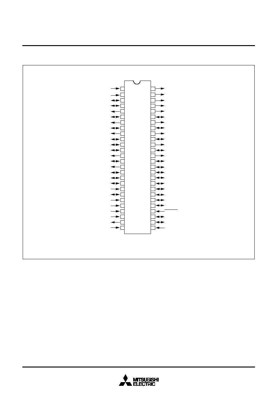
4. PIN CONFIGURATION
Outline 52P4B
Fig. 4.1 Pin Configuration (Top View)
22
23
24
25
26
31
30
29
28
27
1
2
3
4
5
6
7
8
9
10
11
12
13
14
15
16
17
18
19
20
21
52
51
50
49
48
47
46
45
44
43
42
41
40
39
38
37
36
35
34
33
32
P0
6
/INT2/AD4
X
OUT
P5
0
/H
SYNC
P5
1
/V
SYNC
P0
0
/PWM0
P0
1
/PWM1
P0
2
/PWM2
P0
3
/PWM3
P0
4
/PWM4
P0
5
/PWM5
P0
7
/INT1
P2
3
/TIM3
P2
4
/TIM2
P2
5
AV
CC
HLF
V
HOLD
CV
IN
CNV
SS
X
IN
V
SS
P5
2
/R
P5
3
/G
P5
4
/B
P5
5
/OUT1
P2
0
/S
CLK
P2
1
/S
OUT
P2
2
/S
IN
P1
0
/OUT2
P1
1
/SCL1
P1
2
/SCL2
P1
3
/SDA1
P1
4
/SDA2
P1
5
/AD1/INT3
P1
6
/AD2
P3
0
/AD5
P3
1
/AD6
RESET
P2
6
/OSC1/X
CIN
P2
7
/OSC2/X
COUT
V
CC
P1
7
/AD3
P6
3
P6
4
P6
5
P6
6
P6
7
P5
6
P5
7
P6
0
P6
1
P6
2
M37273M8-XXXSP,M37273MF-XXXSP
M37273E8SP,M37273EFSP
4
SINGLE-CHIP 8-BIT CMOS MICROCOMPUTER with CLOSED CAPTION DECODER
and ON-SCREEN DISPLAY CONTROLLER
M37273M8XXXSP, M37273MFXXXSP
M37273E8SP, M37273EFSP
MITSUBISHI MICROCOMPUTERS
Rev. 1.0
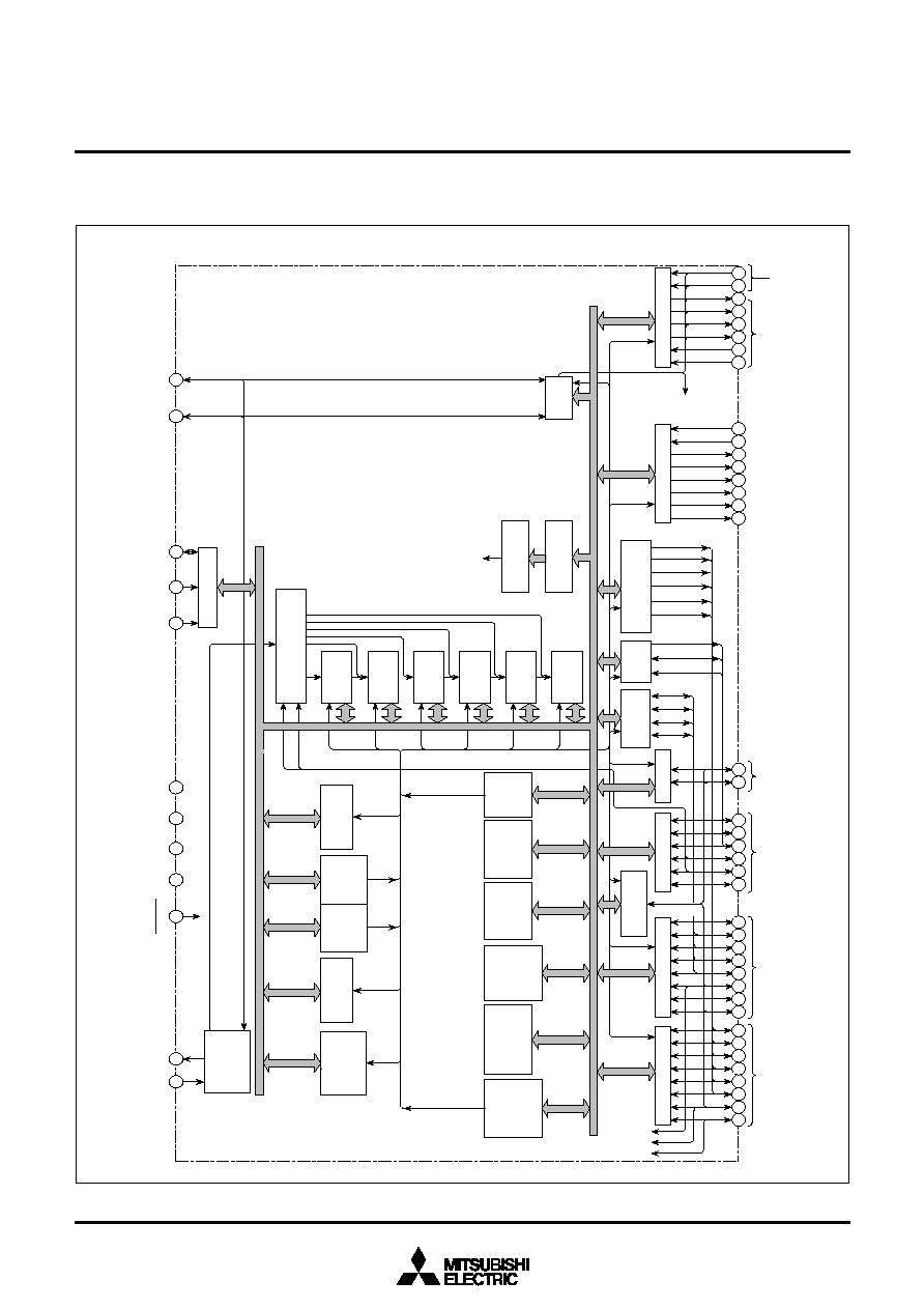
5. FUNCTIONAL BLOCK DIAGRAM
Fig. 5.1 Functional Block Diagram of M37273
X
IN
X
OUT
OSC1/X
CIN
OSC2/X
COUT
P0 (8)
INT1
INT2
INT3
P1 (8)
PWM5
PWM4
PWM3
PWM2
PWM1
PWM0
PWM
TIM2
TIM3
24
25
30
19
27
26
23
CV
IN
22
21
20
V
HOLD
HLF
29
28
14
12
11
10
8
6
4
3
3
3
3
4
3
5
3
6
37
38
39
41
P2 (6)
18
17
16
43
45
I/O port P1
I/O port P2
P3 (2)
32
31
47
SDA2
SDA1
SCL2
SCL1
SI/O
S
IN
S
CLK
S
OUT
49
50
51
52
2
Output ports P5
2
P5
7
Output for display
1
H
SYNC
V
SYNC
R
G
B
OUT1
OUT2
P1
0
I/O ports P3
0
, P3
1
AD1AD6
Data slicer
Control signal
Clock input
Clock output
X
IN
X
OUT
Reset input
AV
CC
V
CC
V
SS
CNV
SS
Pins for data slicer
Clock output for OSD/
sub-clock output
I/O ports P2
6
, P2
7
Clock input for OSD/
sub-clock input
A-D
comparator
8-bit
arithmetic
and
logical unit
Accumulator
A (8)
Timer 6
T6 (8)
Timer 5
T5 (8)
Timer 4
T4 (8)
Timer 3
T3 (8)
Timer 2
T2 (8)
Timer 1
T1 (8)
Timer count source
selection circuit
Instruction
register (8)
Instruction
decoder
CRT
circuit
Processor
status
register
PS (8)
Stack
pointer
S (8)
Index
register
Y (8)
Index
register
X (8)
ROM
32 K bytes
Program
counter
PC
L
(8)
Progam
counter
PC
H
(8)
RAM
1152 bytes
Data bus
Clock
generating
circuit
RESET
CV
IN
Address bus
I/O port P0
ROM
correction
circuit
Multi-master
I2
C-BUS
interface
Input ports P5
0
, P5
1
Synchronous signal input
P5 (8)
75
44
46
48
15
13
9
P6 (8)
40
42
Output ports P6
5
SINGLE-CHIP 8-BIT CMOS MICROCOMPUTER with CLOSED CAPTION DECODER
and ON-SCREEN DISPLAY CONTROLLER
M37273M8XXXSP, M37273MFXXXSP
M37273E8SP, M37273EFSP
MITSUBISHI MICROCOMPUTERS
Rev. 1.0
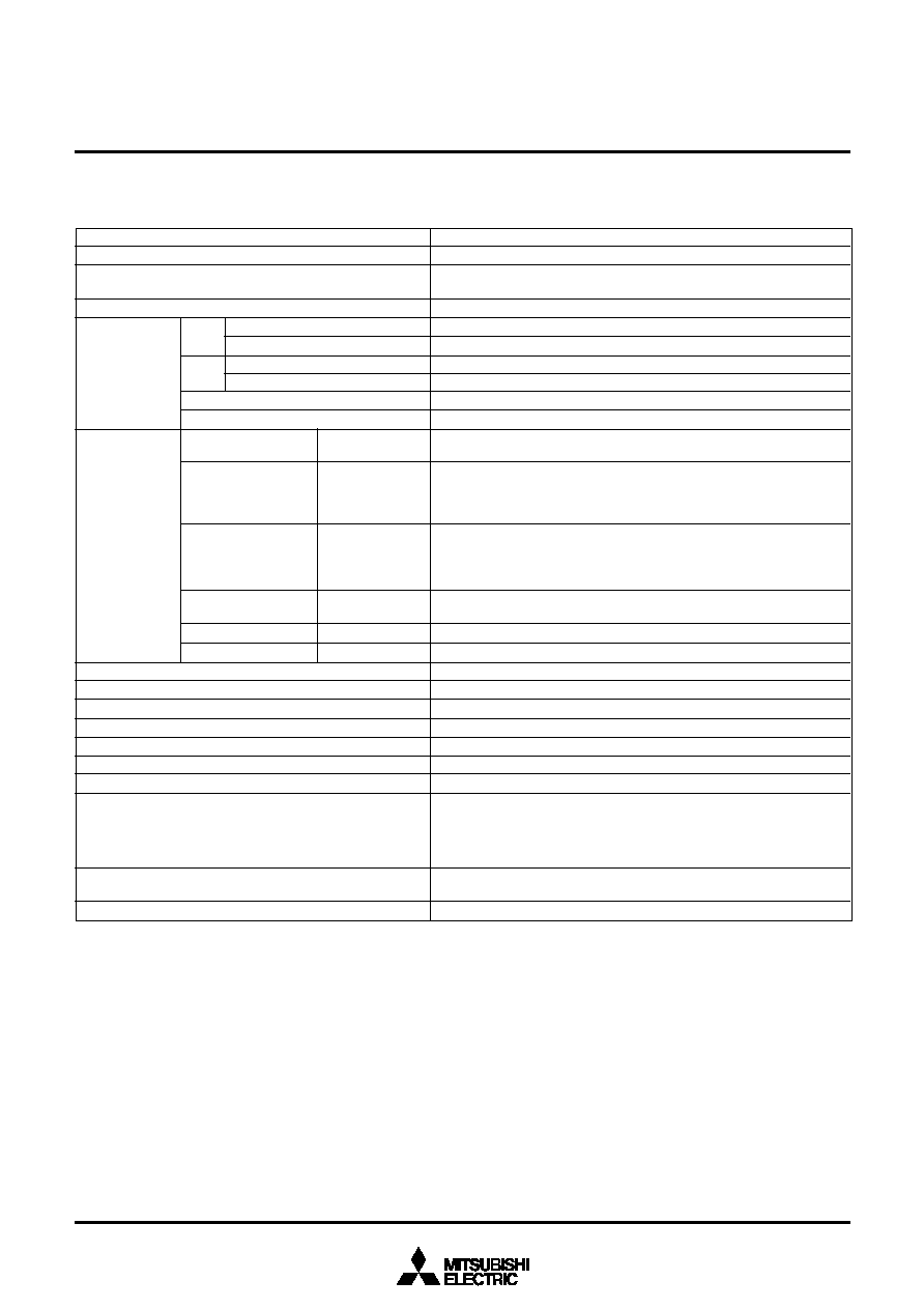
Number of basic instructions
Instruction execution time
Clock frequency
Memory size
Input/Output
ports
Serial I/O
Multi-master I
2
C-BUS interface
A-D comparator
PWM output circuit
Timers
ROM correction function
Subroutine nesting
Interrupt
Clock generating circuit
Data slicer
ROM
RAM
OSD ROM
OSD RAM
P0
P1
0
P1
7
P2
0
P2
7
P3
0
, P3
1
P5
0
, P5
1
P5
2
P5
5
,P6
M37273M8-XXXSP, M37273E8SP
M37273MF-XXXSP, M37273EFSP
M37273M8-XXXSP, M37273E8SP
M37273MF-XXXSP, M37273EFSP
I/O
I/O
I/O
I/O
Input
Output
71
0.5
µ
s (the minimum instruction execution time, at 8 MHz oscillation fre-
quency)
8 MHz (maximum)
32K bytes
60K bytes
1152 bytes (ROM correction memory included)
1472 bytes (ROM correction memory included)
10K bytes
128 bytes
8-bit
!
1 (N-channel open-drain output structure, can be used as PWM
output pins, INT input pins, A-D input pin)
8-bit
!
1 (CMOS input/output structure, however, N-channel open-drain
output structure, when P1
1
P1
4
are used as multi-master I
2
C-BUS inter-
face, can be used as OSD output pin, A-D input pins, INT input pin, multi-
master I
2
C-BUS interface)
8-bit
!
1 (P2 is CMOS input/output structure, however, N-channel open-
drain output structure when P2
0
and 2
1
are used as serial output, can be
used as serial input/output pins, timer external clock input pins, OSD clock
input/output pin, sub-clock input/output pins)
2-bit
!
1 (CMOS input/output or N-channel open-drain output structure,
can be used as A-D input pins)
2-bit
!
1 (can be used as OSD input pins)
14-bit
!
1 (CMOS output structure, can be used as OSD output pins)
8-bit
!
1
1 (2 systems)
6 channels (6-bit resolution)
8-bit
!
6
8-bit timer
!
6
2 vectors
128 levels (maximum)
<17 types>
INT external interrupt
!
3, Internal timer interrupt
!
6, Serial I/O interrupt
!
1, OSD interrupt
!
1, Multi-master I
2
C-BUS interface interrupt
!
1, Data
slicer interrupt
!
1, f(X
IN
)/4096 interrupt
!
1, V
SYNC
interrupt
!
1, BRK
instruction interrupt
!
1, reset
!
1
2 built-in circuits (externally connected to a ceramic resonator or a quartz-
crystal oscillator)
Built-in
Parameter
6. PERFORMANCE OVERVIEW
Table 6.1 Performance Overview
Functions
Document Outline
- Be sure to read
- Table of Contents
- SFR
- PDF Revision History