
CDC 3257G-C2
Automotive Controller
Edition Dec. 5, 2003
6251-634-1AI
ADVANCE INFORMATION
MICRONAS
MICRONAS

CDC 3257G-C2
ADVANCE INFORMATION
2
Dec. 5, 2003; 6251-634-1AI
Micronas
Contents
Page
Section
Title
3
1.
Introduction
3
1.1.
Features
5
1.2.
Abbreviations
6
1.3.
Block Diagram
7
2.
Packages and Pins
7
2.1.
Package Outline Dimensions
8
2.2.
Pin Assignment
8
2.3.
Pin Function Description (differing from CDC32xxG-C User Manual)
9
2.4.
External Components
10
3.
Electrical Data
10
3.1.
Absolute Maximum Ratings
11
3.2.
Recommended Operating Conditions
12
3.3.
Characteristics
14
3.4.
Recommended Quartz Crystal Characteristics
15
4.
CPU and Clock System
16
5.
Memory and Special Function ROM (SFR) System
17
6.
Core Logic
17
6.1.
Control Word (CW)
18
7.
IRQ Interrupt Controller Unit (ICU)
19
8.
Hardware Options
19
8.1.
Functional Description
20
9.
Register Cross Reference Table
20
9.1.
8-Bit I/O Region
25
9.2.
32-Bit I/O Region
26
9.3.
Modified Registers
28
10.
Data Sheet History

ADVANCE INFORMATION
CDC 3257G-C2
Micronas
Dec. 5, 2003; 6251-634-1AI
3
1. Introduction
The device is a microcontroller for use in automotive applica-
tions. The on-chip CPU is an ARM
processor ARM7TDMI
with 32-bit data and address bus, which supports Thumb
format instructions.
The chip contains timer/counters, interrupt controller, multi
channel AD converter, stepper motor and LCD driver, CAN
interfaces and PWM outputs and a crystal clock multiplying
PLL.
This document provides MCM Flash hardware specific infor-
mation. General information on operating the IC can be
found in the document "CDC32xxG-C Hardware Manual and
CDC3205G-C Data Sheet (1PD)".
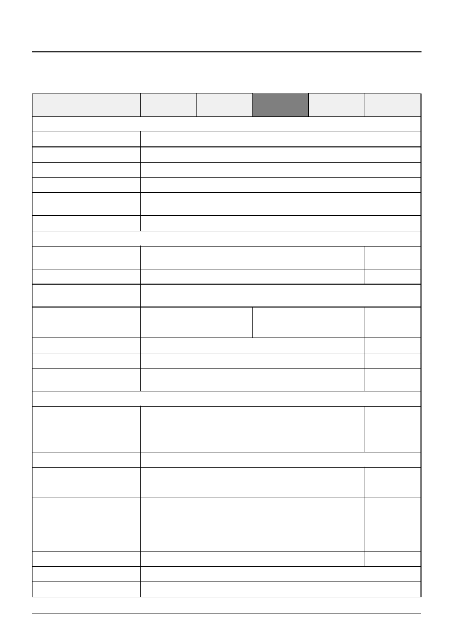
1.1. Features
Table 1≠1: CDC32xxG-C Family Feature List
This Device:
Item
CDC3205G-C
EMU
CDC3207G-C
MCM Flash
CDC3257G-C2
MCM Flash
CDC3272G-C
Mask ROM
CDC3231G-C
Mask ROM
Core
CPU
32-bit ARM7TDMI
CPU-Active Operation Modes
DEEP SLOW, SLOW, FAST and PLL
Power Saving Modes (CPU Inac-
tive)
IDLE, WAKE and STANDBY
CPU clock multiplication
PLL delivering up to 50MHz
EMI Reduction Mode
selectable in PLL mode
Oscillators
4 to 5MHz Quartz and 20 to 50kHz Internal RC
RAM, zero wait state, 32 bit wide
32kByte 12kByte
16kByte
6kByte
ROM
ROMless, ext.
up to
4M x 32/
8M x 16
512-kByte
Flash (256K x
16) top boot
conf.
256-kByte
Flash (128K x
16) top boot
conf.
384kByte
(96K x 32/
192K x 16)
128kByte
(32K x 32/
64K x 16)
Boot ROM
8kByte (Special Function ROM)
Digital Watchdog
Central Clock Divider
Interrupt Controller expanding
IRQ
40 inputs, 16 priority levels
26 inputs, 16
priority levels
Port Interrupts including Slope
Selection
6 inputs
5 inputs
Port Wake-Up Inputs including
Slope / Level Selection
10 inputs
Patch Module
10 ROM locations
Boot System
allows in-system downloading of external code to
Flash memory via JTAG
-
Device Lock Module
Inhibits Access to internal Firmware, Lock settable
by Customer
-
CDC 3257G-C2
ADVANCE INFORMATION
4
Dec. 5, 2003; 6251-634-1AI
Micronas
Analog
Reset/Alarm
Combined Input for Regulator Input Supervision
Clock and Supply Supervision
10-bit ADC, charge balance type
16 channels (each selectable as digital input)
ADC Reference
VREF Pin, P1.0 Pin, P1.1 Pin or VREFINT Internal Bandgap selectable
Comparators
P06COMP with 1/2 AVDD reference,
WAITCOMP with Internal Bandgap reference
LCD
Internal processing of all analog voltages for the LCD driver
Communication
DMA
3 DMA Channels, one each for serving the Graphics Bus interface,
SPI0 and SPI1
-
UART
2: UART0 and UART1
UART0
Synchronous Serial Peripheral
Interfaces
2: SPI0 and SPI1, DMA supported
Full CAN modules V2.0B
with 512-byte object RAM each
(LCAN000E)
4: CAN0, CAN1, CAN2 and CAN3
2: CAN0 and CAN1
1: CAN0
DIGITbus
1 master module
-
I
2
C
2 master modules: I2C0 and I2C1
I2C0
Graphics Bus Interface
8-bit data bus, DMA supported, e.g. for connection of EPSON SED
1560 LCD controller
-
Input & Output
Universal Ports selectable as 4:1
mux LCD Segment/Backplane
lines or Digital I/O Ports
up to 52 I/O or 48 LCD segment lines (=192 segments),
individually configurable as I/O or LCD
up to 50 I/O or
46LCD seg-
ment lines
(=184 seg-
ments)
Universal Port Slew Rate
SW selectable
Stepper Motor Control Modules
with High-Current Ports
7 Modules,
32 dI/dt controlled ports
4 Modules
23 dI/dt con-
trolled ports
PWM Modules, each config-
urable as two 8-bit PWMs or one
16-bit PWM
6 Modules: PWM0/1, PWM2/3, PWM4/5, PWM6/7, PWM8/9 and
PWM10/11
5 Modules:
PWM0/1,
PWM2/3,
PWM4/5,
PWM6/7,
PWM8/9
Phase-Frequency Modulator
2: PFM0 and PFM1
-
Audio Module with auto-decay
SW selectable Clock outputs
2
Table 1≠1: CDC32xxG-C Family Feature List
This Device:
Item
CDC3205G-C
EMU
CDC3207G-C
MCM Flash
CDC3257G-C2
MCM Flash
CDC3272G-C
Mask ROM
CDC3231G-C
Mask ROM

ADVANCE INFORMATION
CDC 3257G-C2
Micronas
Dec. 5, 2003; 6251-634-1AI
5
ARM
and Thumb
are the registered trademarks of ARM Limited.
ARM7TDMI
is the trademark of ARM Limited.
1.2. Abbreviations
ADC
Analog-to-Digital Converter
AM
Audio Module
CAN
Controller Area Network Module
CAPCOM
Capture/Compare Module
CCC
Capture/Compare Counter
CPU
Central Processing Unit
DMA
Direct Memory Access Module
ERM
EMI Reduction Mode
ETM
Embedded Trace Module
I2C
I
2
C Interface Module
LCD
Liquid Crystal Display Module
P06COMP
P0.6 Alarm Comparator
PWM
Pulse Width Modulator Module
SM
Stepper Motor Control Module
SPI
Serial Synchronous Peripheral Interface
T
Timer
UART
Universal Asynchronous Receiver Transmitter
WAITCOMP Wait Comparator
Polling / Flash Timer Output
1 High-Current Port output operable in Power Saving Modes
Timers & Counters
16-bit free running counters with
Capture/Compare modules
CCC0 with 4 CAPCOM
CCC1 with 2 CAPCOM
CCC0 with 4
CAPCOM
16-bit timers
1: T0
8-bit timers
4: T1, T2, T3 and T4
Real Time Clock, Delivering
Hours, Minutes and Seconds
Miscellaneous
Scalable layout in CAN, RAM
and ROM
-
Various randomly selectable HW
options
Set by copy from user program storage during system start-up
JTAG interface
allows Flash programming
On Chip Debug Aids
Embedded
Trace Module,
JTAG
JTAG
Core Bond-Out
-
Supply Voltage
3.5 to 5.5V (limited I/O performance below 4.5V)
Case Temperature Range
0 to +70C
-40 to +105C
Package
Type
Ceramic
257PGA
Plastic 128QFP
0.5mm pitch
Bonded Pins
256
128
128
126
111
Table 1≠1: CDC32xxG-C Family Feature List
This Device:
Item
CDC3205G-C
EMU
CDC3207G-C
MCM Flash
CDC3257G-C2
MCM Flash
CDC3272G-C
Mask ROM
CDC3231G-C
Mask ROM