 | –≠–ª–µ–∫—Ç—Ä–æ–Ω–Ω—ã–π –∫–æ–º–ø–æ–Ω–µ–Ω—Ç: RFRXD0920 | –°–∫–∞—á–∞—Ç—å:  PDF PDF  ZIP ZIP |

2003 Microchip Technology Inc.
Preliminary
DS70090A-page 1
rfRXD0420/0920
Features:
∑ Low cost single conversion superheterodyne
receiver architecture
∑ Compatible with rfPICTM and rfHCS series of RF
transmitters
∑ Easy interface to PICmicro
Æ
microcontroller
(MCU) and K
EE
L
OQÆ
decoders
∑ VCO phase locked to quartz crystal reference:
- Narrow receiver bandwidth
- Maximizes range and interference immunity
∑ Selectable LNA gain control for improved dynamic
range
∑ Selectable IF bandwidth via external ceramic IF
filter
∑ Received Signal Strength Indicator (RSSI) for
signal strength indication (FSK, FM) and ASK
demodulation
∑ FSK/FM quadrature (phase coincidence) detector
demodulator
∑ 32-Lead LQFP package
UHF ASK/FSK Receiver:
∑ Single frequency receiver set by crystal frequency
∑ Receive frequency range:
∑ Maximum data rate:
- ASK: 80 Kbps NRZ
- FSK: 40 Kbps NRZ
∑ IF frequency range: 455 kHz to 21.4 MHz
∑ RSSI range: 70 dB
∑ Frequency deviation range: ±5 kHz to ±120 kHz
∑ Maximum FM modulation frequency: 15 kHz
Pin Diagram:
Applications:
∑ Wireless remote command and control
∑ Wireless security systems
∑ Remote Keyless Entry (RKE)
∑ Low power telemetry
∑ Low power FM receiver
∑ Home automation
∑ Remote sensing
Bi-CMOS Technology:
∑ Wide operating voltage range
∑ Low current consumption in Active and Standby
modes
- rfRXD0420
- 8.2 mA (typical, LNA High Gain mode)
- <100 nA standby
- rfRXD0920
- 9.2 mA (typical, LNA High Gain mode)
- <100 nA standby
∑ Wide temperature range:
- Industrial: -40∞C to +85∞C
Device
Frequency Range
rfRXD0420
300 MHz to 450 MHz
rfRXD0920
800 MHz to 930 MHz
2
3
4
5
6
1
15 16
9 10 11 12
29
8
7
32 31 30
13 14
23
24
17
18
19
20
21
22
27
25
26
28
DEM
IN
2IF
OU
T
1IF
OUT
V
DD
FBC2
FBC1
2IF
IN
V
SS
V
DD
LNA
IN
V
SS
LF ENRX V
DD
XT
AL
V
SS
DEM
OUT
-
DEM
OUT
+
V
SS
RSSI
OPA+
OPA-
OPA
V
DD
V
SS
LNA
GAIN
LNA
OUT
1IF
IN
V
SS
1IF+
1IF-
V
DD
rfRXD0420
LQFP
rfRXD0920
UHF ASK/FSK/FM Receiver

rfRXD0420/0920
DS70090A-page 2
Preliminary
2003 Microchip Technology Inc.
1.0
DEVICE OVERVIEW
The rfRXD0420/0920 are low cost, compact single
frequency short-range radio receivers requiring only a
minimum number of external components for a
complete receiver system. The rfRXD0420 covers the
receive frequency range of 300 MHz to 450 MHz and
the rfRXD0920 covers 800 MHz to 930 MHz. The
rfRXD0420 and rfRXD0920 share a common architec-
ture. They can be configured for Amplitude Shift Keying
(ASK), Frequency Shift Keying (FSK), or FM modula-
tion. The rfRXD0420/0920 are compatible with rfPICTM
and rfHCS series of RF transmitters.
∑ High frequency stability over temperature and
power supply variations
∑ Low spurious signal emission
∑ High large-signal handling capability with
selectable LNA gain control for improved dynamic
range
∑ Selectable IF bandwidth via external low cost
ceramic IF filter. The IF Frequency range is
selectable between 455 kHz to 21.4 MHz. This
facilitates the use of readily available low cost
10.7 MHz ceramic IF filters in a variety of
bandwidths.
∑ ASK or FSK for digital data reception
∑ FM modulation for analog signal reception
∑ FSK/FM demodulation using quadrature detector
(phase coincidence detector)
∑ Received Signal Strength Indication (RSSI) for
signal strength indication and ASK detection
∑ Wide supply voltage range
∑ Low active current consumption
∑ Very low standby current
The rfRXD0420/0920 is a single conversion superhet-
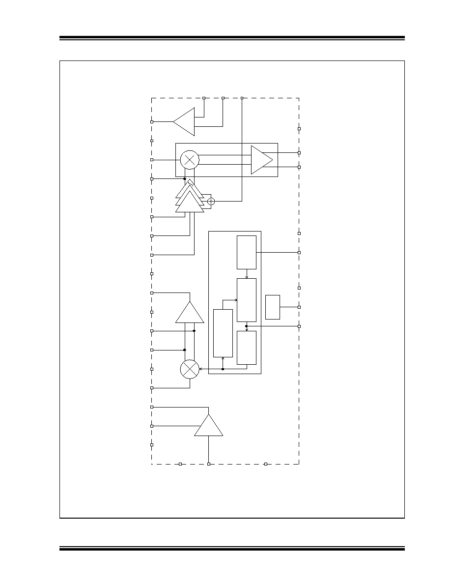
erodyne architecture. A block diagram is illustrated in
Figure 1-1. The rfRXD0420/0920 consists of:
∑ Low-noise amplifier (LNA) - Gain selectable
∑ Mixer for down-conversion of the RF signal to the
Intermediate Frequency (IF) followed by an IF
preamplifier
∑ Fully integrated Phase-Locked Loop (PLL)
frequency synthesizer for generation of the Local
Oscillator (LO) signal. The frequency synthesizer
consists of:
- Crystal oscillator
- Phase-frequency detector and charge pump
- High-frequency Voltage Controlled Oscillator
(VCO)
- Fixed feedback divider
- rfRXD0420 = divide by 16
- rfRXD0920 = divide by 32
∑ IF limiting amplifier to amplify and limit the IF
signal and for Received Signal Strength Indication
(RSSI) generation
∑ Demodulator (DEMOD) section consists of a
phase detector (MIXER2) and amplifier creating a
quadrature detector (also known as a phase
coincidence detector) to demodulate the IF signal
in FSK and FM modulation applications
∑ Operational amplifier (OPA) that can be config-
ured as a comparator for ASK or FSK data
decision or as a filter for FM modulation.
∑ Bias circuitry for bandgap biasing and circuit
shutdown
2003 Microchip Technology Inc.
Preliminary
DS70090A-page 3
rfRXD0420/0920
FIGURE 1-1:
rfRXD0420/0920 BLOCK DIAGRAM
LNA
LNA
LNA
1IF
31
34
1IF+
1IF-
7
6
9
11
12
13
21
1IF
2IF
FBC1
FBC2
RSSI
20
19
18
OPA+
OPA-
OPA
XTAL
LF
29
26
Bias
ENRX
28
LNA
2
OPA
16
15
2IF
DEM
+
-
-
+-
OUT+
OUT-
24
23
DEMOD
IN
OUT
IN
OUT
IN
GAIN
OUT
IN
V
SS
1
V
SS
5
V
DD
8
V
SS
10
V
DD
14
V
DD
17
V
DD
32
V
SS
30
27
V
DD
25
V
SS
DEM
DEM
MIXER1
IF Preamp
IF Limiting Amplifier
MIXER2
22
V
SS
with RSSI
Crystal
Oscillator
Phase Detector
and
Charge Pump
Voltage
Controlled
Oscillator
Fixed Divide by
Frequency
Synthesizer
16: rfRXD0420
32: rfRXD0920

rfRXD0420/0920
DS70090A-page 4
Preliminary
2003 Microchip Technology Inc.
TABLE 1-1:
rfRXD0420/0920
PINOUT I/O DESCRIPTION
Pin Name
Pin Number
Pin Type
Buffer Type
Description
LNA
GAIN
2
I
CMOS
LNA gain control (with hysteresis)
LNA
OUT
3
O
Analog
LNA output (open collector)
1IF
IN
4
I
Analog
1st IF stage input
1IF+
6
--
Analog
MIXER1 bias (open collector)
1IF-
7
--
Analog
MIXER1 bias (open collector)
1IF
OUT
9
O
Analog
1st IF stage output
2IF
IN
11
I
Analog
2nd IF stage input
FBC1
12
--
Analog
Limiter IF Amplifier external feedback capacitor
FBC2
13
--
Analog
Limiter IF Amplifier external feedback capacitor
2IF
OUT
15
O
Analog
2nd IF stage output
DEM
IN
16
I
Analog
Demodulator input
OPA
18
O
Analog
Operational amplifier output
OPA-
19
I
Analog
Operational amplifier input (negative)
OPA+
20
I
Analog
Operational amplifier input (positive)
RSSI
21
O
Analog
Received signal strength indicator output
DEM
OUT
+
23
O
Analog
Demodulator output (positive)
DEM
OUT
-
24
O
Analog
Demodulator output (negative)
XTAL
26
I
Analog
Crystal oscillator input
ENRX
28
I
CMOS
Receiver enable input
LF
29
I
Analog
External loop filter connection. Common node of
charge pump output and VCO tuning input.
LNA
IN
31
I
Analog
LNA input
V
DD
8, 14, 17, 27, 32
P
Positive supply
V
SS
1, 5, 10, 25, 30
P
Ground reference
Legend: I = Input, O = Output, I/O = Input/Output, P = Power, CMOS = CMOS compatible input or output

2003 Microchip Technology Inc.
Preliminary
DS70090A-page 5
rfRXD0420/0920
2.0
CIRCUIT DESCRIPTION
This section gives a circuit description of the internal
circuitry of the rfRXD0420/0920 receiver. External
connections and components are given in the
APPLICATION CIRCUITS section.
2.1
Bias Circuitry
Bias circuitry provides bandgap biasing and circuit
shutdown capabilities. The ENRX (Pin 28) modes are
summarized in Table 2-1. The ENRX pin is a CMOS
compatible input and is internally pulled down to Vss.
2.2
Frequency Synthesizer
The Phase-locked Loop (PLL) frequency synthesizer
generates the Local Oscillator (LO) signal. It consists
of:
∑ Crystal oscillator
∑ Phase-frequency detector and charge pump
∑ Voltage Controlled Oscillator (VCO)
∑ Fixed feedback divider:
- rfRXD0420 = divide by 16
- rfRXD0920 = divide by 32
2.2.1
CRYSTAL OSCILLATOR
The internal crystal oscillator is a Colpitts type oscilla-
tor. It provides the reference frequency to the PLL. A
crystal is normally connected to the XTAL (Pin 26) and
ground. The internal capacitance of the crystal oscilla-
tor is 15 pF. Alternatively, a signal can be injected into
the XTAL pin from a signal source. The signal should
be AC coupled via a series capacitor at a level of
approximately 600 mV
pp
.
The XTAL pin is illustrated in Figure 2-1.
FIGURE 2-1:
BLOCK DIAGRAM OF
XTAL PIN
The PLL consists of a phase-frequency detector,
charge pump, voltage-controlled oscillator (VCO), and
fixed divide-by-16 (rfRXD0420) or divide-by-32
(rfRXD0920) divider. The rfRXD0420/0920 employs a
charge pump PLL that offers many advantages over
the classical voltage phase detector PLL: infinite pull-in
range and zero steady state phase error. The charge
pump PLL allows the use of passive loop filters that are
lower cost and minimize noise. Charge pump PLLs
have reduced flicker noise thus limiting phase noise.
An external loop filter is connected to pin LF (Pin 29).
The loop filter controls the dynamic behavior of the
PLL, primarily lock time and spur levels. The applica-
tion determines the loop filter requirements.
The VCO gain for the rfRXD0420/0920 receivers are
listed in Table 2-2.
The LF pin is illustrated in Figure 2-2.
FIGURE 2-2:
BLOCK DIAGRAM OF LOOP
FILTER PIN
2.3
Low Noise Amplifier
The Low-Noise Amplifier (LNA) is a high-gain amplifier
whose primary purpose is to lower the overall noise
figure of the entire receiver thus enhancing the receiver
sensitivity. The LNA is an open-collector cascode
design. The benefits of a cascode design are:
∑ high gain with low noise
∑ high-frequency
∑ wide bandwidth
∑ low effective input capacitance with stable input
impedance
∑ high output resistance
∑ high reverse isolation that provides improved
stability and reduces LO leakage
TABLE 2-1:
BIAS CIRCUITRY CONTROL
ENRX
(1)
Description
0
Standby mode
1
Receiver enabled
Note 1: ENRX has internal pull-down to Vss
XTAL
26
40 µA
V
SS
V
SS
V
SS
30 pF
30 pF
50 k
V
DD
V
DD
V
DD
TABLE 2-2:
PLL PARAMETERS
Device
K
VCO(1)
I
CP(1)
Divider
rfRXD0420
250 MHz/V at
433 MHz
60
µA
16
rfRXD0920
300 MHz/V at
868 MHz
60
µA
32
Note 1: Typical value
LF
29
V
SS
V
SS
V
SS
4 pF
200
400
V
DD