 | –≠–ª–µ–∫—Ç—Ä–æ–Ω–Ω—ã–π –∫–æ–º–ø–æ–Ω–µ–Ω—Ç: ML4895 | –°–∫–∞—á–∞—Ç—å:  PDF PDF  ZIP ZIP |

August 1996
PRELIMINARY
ML4895
Synchronous Buck Controller
1
FEATURING
Extended Commercial Temperature Range
-20∞C to 70∞C
for Portable Handheld Equipment
BLOCK DIAGRAM
FEATURES
s
Regulation to ±3% maximum
s
Adjustable output synchronous buck (2.5V to 4V)
s
Wide input voltage range (5.9V to 15V)
s
Power conversion efficiencies of >90% over 3 decades
of output current
s
Integrated antishoot-through logic
s
Shutdown control provides load isolation and
minimum sleep mode power consumption
s
Low shutdown current
P DRV
N DRV
VOUT
2.5V - 4V
+
≠
ISENSE
VFB
8
1
FROM SYSTEM
POWER
MANAGEMENT
GND
VREG
V
I
N
BIAS
CIRCUITS
SHDN
5
7
6
3
2
VIN
5.9V - 15V
4
BUCK REGULA
TOR
SLEEP
LOGIC
GENERAL DESCRIPTION
The ML4895 synchronous buck controller has been
designed to provide high efficiency DC/DC conversion for
portable products. The ML4895 can deliver a user
programmable 2.5V to 4V output from input voltages of
5.9V to 15V.
The ML4895 drives external P- and N-channel MOSFETs
in a synchronous buck topology, allowing an overall
conversion efficiency of greater than 90% over an output
current range exceeding three decades, with an output
current capability of up to 5A.
The regulator can be disabled via the SHDN pin. While
disabled, the output of the regulator is completely
isolated from the circuit's input supply, and the supply
current is reduced to less than 5µA to help extend battery
life.

ML4895
2
PIN CONFIGURATION
PIN DESCRIPTION
PIN# NAME
FUNCTION
1
V
REG
Connection point for internal linear
regulator bypass capacitor
2
V
FB
Programming pin for setting the
output voltage
3
I
SENSE
Current sense input
4
SHDN
a logic low on this pin shuts down the
regulator and all internal bias
circuitry for minimum power
consumption
ML4895
8-Pin SOIC (S08)
PIN# NAME
FUNCTION
5
GND
Analog signal ground
6
N DRV
NMOS driver output
7
P DRV
PMOS driver output
8
V
IN
Battery input voltage
1
2
3
4
8
7
6
5
VREG
VFB
ISENSE
SHDN
VIN
P DRV
N DRV
GND
TOP VIEW

ML4895
3
ELECTRICAL CHARACTERISTICS
Unless otherwise specified, V
IN
= 10V, T
A
= Operating Temperature Range (Note 1)
PARAMETER
CONDITIONS
MIN
TYP
MAX
UNITS
LINEAR REGULATOR
Output Voltage
T
A
= 25∞C
3.29
3.33
3.37
V
Line Regulation
5.9V < V
IN
< 15V
1.7
4
mV/V
Total Variation
Line, Temp
3.24
3.42
V
SHUTDOWN
Input Low Voltage
1.0
V
Input High Voltage
3.0
V
Input Low Current
V
IL
= 0V
100
nA
Input High Current
V
IH
= V
IN
50
µ
A
BUCK REGULATOR
Duty Cycle Ratio
V
IN
= 5.9V, I
SENSE
= V
FB
= 0V
75
97
%
V
FB
Threshold Voltage
5.9V < V
IN
< 15V
2.425
2.5
2.575
V
I
SENSE
Threshold Voltage
-60
-80
-100
mV
Transition Time
C
L
= 1000 pF, GND to V
IN
50
100
ns
SUPPLY
V
IN
Current
SHDN = 0V
2
5
µ
A
SHDN = 5V
300
750
µ
A
ABSOLUTE MAXIMUM RATINGS
Absolute maximum ratings are those values beyond
which the device could be permanently damaged.
Absolute maximum ratings are stress ratings only and
functional device operation is not implied.
V
IN ............................................................................................
16.5V
Peak Driver Output Current....................................... ±2A
V
FB
Voltage .........................................GND - 0.3V to 6V
I
SENSE
Voltage ..................................................... +500mV
All Other Inputs ..................... GND - 0.3V to V
IN
+ 0.3V
SHDN Input Current ............................................. 100
µ
A
Note 1:
Limits are guaranteed by 100% testing, sampling, or correlation with worst case test conditions.
Junction Temperature............................................. 150∞C
Storage Temperature Range .....................≠65∞C to 150∞C
Lead Temperature (Soldering, 10 sec) .................... 150∞C
Thermal Resistance (
JA
) ....................................160∞C/W
OPERATING CONDITIONS
V
IN
Range .................................................... 5.9V to 15V
V
OUT
Range ................................................... 2.5V to 4V
Temperature Range ................................... -20∞C to 70∞C

ML4895
4
FUNCTIONAL DESCRIPTION
The ML4895 converts a 5.9V to 15V input to an
adjustable 2.5V to 4V output using a unique current
mode PFM synchronous buck control architecture. The
output current is set by external components, and can
exceed 2A. Even at light loads, the PFM architecture
maintains high conversion efficiencies over a wide range
of input voltages. If it is necessary to further extend
battery life, the user can shutdown and fully disconnect
the load from the input when the supply is not in use.
BIAS CIRCUITS
The bias circuits are comprised of a linear regulator and a
precision 2.5V reference. The V
REG
pin should be
bypassed to GND with a 1µF capacitor. The 2.5V
reference is used by the feedback circuit of the controller
to maintain an accurate output voltage.
SHUTDOWN LOGIC
The ML4895 is shut down by applying a logic low to the
SHDN pin. This prevents switching from occurring and
disconnects the load from the input. The supply current in
shutdown typically ranges from 0.5µA at V
IN
= 5.9V to
3µA at V
IN
= 15V
BUCK CONTROLLER
A block diagram of the buck controller is shown in Figure
1. The circuit utilizes a constant ON-time PFM control
architecture. The circuit determines the OFF-time by
waiting for the inductor current to drop to a level set by
the feedback voltage (V
FB
).
The oscillator/one shot block generates a constant ON-
time and a minimum OFF-time. The OFF-time is extended
for as long as the output of the current comparator stays
low. Note that the inductor current flows in the current
sense resistor during the OFF-time. Therefore, a minimum
OFF-time is required to allow for the finite circuit delays
in sensing the inductor current. The ON-time is triggered
when the current comparator's output goes high.
However, unlike conventional fixed ON-time controllers,
this one shot has an inverse relationship with the input
voltage as shown in Figure 2. Figure 3 plots the inductor
voltage-ON-time product. Note that the volt-second
product is nearly constant over the entire input voltage
range. The inductor current is given by:
I
T
V
V
L
L
ON
IN
OUT
=
◊
-
b
g
(1)
This means that the ripple current also remains nearly
constant over the entire input voltage range.
The transconductance amplifier generates a current from
the voltage difference between the reference and the
feedback voltage, V
FB
. This current produces a voltage
across R
gm
that adds to the negative voltage that is
developed across the current sense resistor. When the
current level in the inductor drops low enough (a less
negative sense voltage) to cause the voltage at the non-
inverting input of the current comparator to go positive,
the comparator trips and starts a new ON cycle. In other
words, the current programming comparator controls the
length of the OFF-time by waiting until the inductor
current decreases to a value determined by the
transconductance amplifier.
This technique allows the feedback transconductance
amplifier's output current to steer the current level in the
inductor. The higher the transconductance amplifier's
output current, the higher the inductor current. For
example, when the output voltage drops due to a load
increase, the transconductance amplifier will increase its
output current and generate a larger voltage across R
gm
,
which in turn raises the inductor current trip level,
shortening the OFF-time. At some level of increasing the
output load, the transconductance amplifier can no
longer continue to increase its output current. When this
occurs, the voltage across R
gm
reaches a maximum and
the inductor current cannot increase. If the inductor
current tries to increase, the voltage developed across the
current sense resistor would become more negative,
causing the non-inverting input of the current comparator
to be negative, which extends the OFF-time and reduces
the inductor current.
If the output voltage is too high, the transconductance
amplifier's output current will eventually become
negative. However, since the inductor current flows in
only one direction (assuming no shoot-through current)
the non-inverting input of the current comparator will
also stay negative. This extends the OFF-time allowing the
inductor current to decrease to zero, causing the
converter to stop operation until the output voltage drops
enough to increase the output current of the
transconductance amp above zero.
In summary, the three operation modes can be defined by
the voltage at the I
SENSE
pin at the end of the OFF-time:
V
SENSE
> 0V - Discontinuous current mode
0V > V
SENSE
> -60mV - Continuous current mode
-60mV > V
SENSE
> -100mV - Current limit
The synchronous rectifier comparator, flip-flop, and NOR
gate make up the synchronous rectifier control circuit.
The synchronous control does not influence the operation
of the main control loop, and operation with a Schottky
diode in place of the synchronous rectifier is possible, but
at a lower conversion efficiency. The synchronous rectifier
(N DRV) is turned on during the minimum OFF-time. N
DRV will remain on until a new ON-time is started or
until the I
SENSE
pin goes above -7mV. When the I
SENSE
pin
goes above -7mV, the current in the inductor has gone to
zero or the buck regulator is operating in discontinuous
current mode (DCM). Therefore, the synchronous rectifier
comparator is used only for DCM operation. A timing
diagram is shown in Figure 4.

ML4895
5
OSCILLATOR
ONE SHOT
L1
2.5V
3
+
≠
VOUT
ISENSE
COUT
R1
R2
VFB
TRANSCONDUCTANCE
AMPLIFIER
+
-
+
-
-7mV
-
+
S
R
Q
Q
CURRENT
COMPARATOR
SHOOT-THRU
PROTECTION
VIN
2
6
N DRV
7
P DRV
Rgm
tON
VSR
SYNCHRONOUS
RECTIFIER
COMPARATOR
RSENSE
IL
CIN
Figure 1. ML4895 Functional Block Diagram
10
8
6
4
2
0
t ON
(
µ
s)
VIN (V)
5
7.5
10
15
12.5
Figure 2. ON-Time vs. Input Voltage
Figure 3. Volt-seconds vs. Input Voltage
30
25
20
15
10
5
0
VOL
T-SECONDS
VIN (V)
5
7.5
10
15
12.5
VOUT = 2.5V
VOUT = 3.3V
VOUT = 4.0V

ML4895
6
Q (ONE SHOT)
INDUCTOR CURRENT (IL)
VSR
tON
VC
Figure 4. One Shot and Synchronous Rectifier Timing
DESIGN CONSIDERATIONS
A typical design can be implemented by using the
following design procedure. Note that this procedure is
not intended to give final values, but to give a good
starting point, and provide the relationships necessary to
make trade-off decisions. Some experimentation will be
necessary to optimize values and to verify that the design
operates over worst case conditions.
DESIGN SPECIFICATIONS
It is important to start with a clear definition of the design
specifications. Make sure the specifications reflect worst
case conditions. Key specifications include the minimum
and maximum input voltage and the output voltage and
load current.
INDUCTOR AND SENSE RESISTOR SELECTION
Figure 5 shows the inductor current of the buck regulator.
The inductor current is made up of two components: the
DC current level set by the transconductance amplifier,
I
SENSE
, and the inductor ripple current,
I
L
. The figure also
shows that I
OUT
is the summation of I
SENSE
and Ω
I
L
.
I
I
I
V
R
T
V
V
L
OUT
SENSE
L
SENSE
SENSE
ON
IN
OUT
=
+
=
+
◊
-
◊
1
2
2
b
g
(3)
Therefore, the selection of the inductance value
determines how much of the output current is made up of
the ripple current. Higher inductor ripple current allows
smaller inductor values, but results in higher peak
currents, lower efficiency, and higher output voltage
ripple.
Inductor ripple currents in the range of 30% to 70% of the
maximum output current are typical. As a good starting
point, set the inductor ripple current to 50% of the
maximum output current:
I
T
V
V
L
F
I
L
ON
IN
OUT
IRC
OUT MAX
=
◊
-
=
◊
b
g
(
)
(4)
where FIRC = ratio of inductor ripple current to the
maximum output current, or:
L
T
V
V
I
ON
IN
OUT
OUT MAX
=
◊
-
◊
b
g
0 5
.
(
)
(5)
Calculate the inductance using the volt-seconds value
given in Figure 3 at the maximum input voltage. Choose
the nearest standard value, realizing the trade-offs
mentioned before. Then, using the inductance value
chosen, determine the actual inductor ripple current at
the maximum and minimum input voltage using Equation
4 and Figure 3.
The sense resistor value can be determined using the
inductor ripple current value calculated above and
Equation 3 rearranged as follows:
R
V
I
I
SENSE
SENSE MIN
OUT MAX
L MIN
=
-
(
)
(
)
(
)
1
2
(6)
Having determined the values for the inductor and sense
resistor, we can now specify the inductor peak current
rating. This value is calculated at current limit and at the
maximum input voltage, and is given by:
I
I
I
L PEAK MAX
SENSE MAX
L MAX
(
(
))
(
)
(
)
=
+
(7)
I
V
R
I
LPEAK MAX
SENSE MAX
SENSE
L MAX
a
f
c
h
a
f
a
f
=
+
I
V
R
I
L PEAK MAX
SENSE
L MAX
a
f
c
h
a
f
=
+
01
.

ML4895
7
ON resistance - gate charge product provides a good
figure of merit by which to compare various MOSFETs,
the lower the figure the better. The internal gate drivers of
the ML4895 can drive over 100nC of total gate charge,
but 60nC to 70nC is a more practical limit to ensure good
switching times.
The drain-source breakdown voltage rating is determined
by the input voltage. For input voltages up to 10V, a drain
to source rating of 20V is acceptable. For input voltages
up to 15V, a drain to source rating of 30V is
recommended. For a more reliable design, look for
MOSFETs that are avalanche rated.
In high current applications, the MOSFET's power
dissipation often becomes a major design factor. The I
2
R
losses generate the largest portion of heat in the MOSFET
package. Make sure that the MOSFETs are within their
rated junction temperature at the maximum ambient
temperature by calculating the temperature rise using the
thermal resistance specifications.
The worst case power dissipation for the P-MOS switch
occurs at the minimum input voltage and is determined
as follows:
P
I
R
P MOS
RMS ON
DS ON
-
=
◊
(
)
(
)
2
(11)
where:
I
V
V
I
I
I
I
RM S ON
OUT
IN MAX
SENSE( MAX
SENSE( MAX
L PEAK MAX
L PEAK MAX
(
)
(
)
)
)
(
(
))
(
(
))
2
2
2
3
=
◊
+
◊
+
F
H
G
I
K
J
The worst case power dissipation for the N-MOS switch
occurs at the maximum input voltage and is determined
using:
P
I
R
N MOS
RMS OFF
DS ON
-
=
◊
(
)
(
)
2
(12)
For reliable operation, the inductor current rating should
exceed the value calculated by 10%-20%.
For future reference, determine the peak inductor current
at the minimum input voltage:
I
I
I
L PEAK MIN
SENSE MIN
L MIN
(
(
))
(
)
(
)
=
+
(8)
I
V
R
I
L PEAK MIN
SENSE MIN
SENSE
L MIN
a
f
c
h
a
f
a
f
=
+
I
V
R
I
L PEAK MIN
SENSE
L MIN
a
f
c
h
a
f
=
+
0 06
.
Now the sense resistor's power rating can be determined.
The sense resistor must be able to carry the peak current
in the inductor during the OFF-time:
P
I
R
R
RMS OFF
SENSE
SENSE
=
◊
(
)
2
(9)
where:
I
V
V
I
I
I
I
RMS OFF
OUT
IN MAX
SENSE(MAX
SENSE(MAX
L PEAK MAX
L PEAK MAX
(
)
(
)
)
)
(
(
))
(
(
))
2
2
2
1
3
=
-
◊
+
◊
+
F
H
G
I
K
J
The final parameter that should be specified is the
winding resistance of the inductor. In general, the
winding resistance should be as low as possible,
preferably in the low m
range. Since the inductor is in
series with the load at all times, the copper losses can be
approximated by:
P
I
R
Cu
OUT
L
=
◊
2
(10)
A good rule of thumb is to allow 2 m
of winding
resistance per
µ
H of inductance.
MOSFET SELECTION
The switching MOSFETs must be logic level types with
the ON resistance specified at V
GS
= 4.5V. In general, the
t
I
L
I
L
I
LPK
I
SENSE
=
V
SENSE
R
SENSE
I
OUT
= I
SENSE
+ 1/2
I
L
T
ON
V
IN ≠
V
OUT
T
OFF
L
V
OUT
L
Figure 5. Buck Regulator Inductor Current
ML4895
8
DESIGN CONSIDERATIONS (cont.)
INPUT CAPACITOR SELECTION
The choice of the input capacitor is based on its ripple
current and voltage ratings rather than its capacitance
value. The input capacitor should be a low ESR type and
located as close to the source of the P-MOS switch as
possible. The input capacitor's ripple current is
determined by the load current and input voltage, with
the worst case condition occurring at V
IN
= 2 x V
OUT
:
I
I
I
V
V
V
V
RMS C
SENSE MAX
L MAX
OUT
IN
OUT
IN
IN
(
)
(
)
(
)
(
)
+
◊
◊
-
1
2
b
g
The capacitor's voltage rating is based on the maximum
input voltage, V
IN(MAX)
. Capacitor manufacturers typically
recommend derating the capacitor voltage rating by 20%
to 50% for aluminum electrolytic types and 50% to 70%
for tantalum types.
In high current applications it may necessary to add a
small 0.1
µ
F ceramic capacitor to bypass V
IN
(pin 8) of the
ML4895.
OUTPUT CAPACITOR SELECTION
The output capacitors determine the loop stability and the
output ripple voltage. Use only low ESR capacitors
intended for switching power supply applications, such as
AVX TPS, Sprague 593D, Sanyo OS-CON, or Nichicon PL
series. To ensure stability, the minimum capacitance value
is given by:
C
V
T
R
OUT
OUT
ON MAX
SENSE
◊
4 3
.
(
)
(14)
The maximum ESR value can be estimated using:
ESR
V
I
OUT
L MAX
(
)
(15)
The selected capacitor must meet both the capacitance
and ESR requirements. As a final check, make sure the
output capacitor can handle the ripple current, I
RMS
:
I
I
RMS
L MAX
(
)
12
(16)
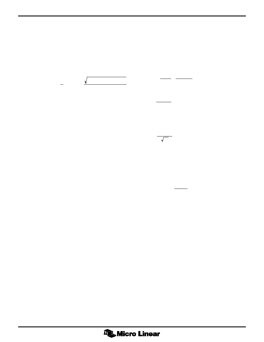
OUTPUT VOLTAGE
The output of the buck converter is adjustable and can be
set to any voltage between 2.5V and 4V by connecting a
resistor divider to the feedback pin as shown in Figure 1.
The resistor values R1 and R2 can be calculated using the
following equation:
V
V
R
R2
R2
OUT
=
◊
+
250
1
.
(17)
The value of R2 should be 475k
or less to minimize bias
current errors.
It is important to note that the accuracy of these resistors
directly affects the accuracy of the output. Use precision
resistors and set the nominal voltage approximately 1% to
2% high in order to make up for the load regulation. This
offset results in the best overall output accuracy over line
and load.

ML4895
9
LAYOUT
A typical application circuit is shown in Figure 6.
Proximity of passive devices and adequate power and
ground planes are critical for reliable operation of the
circuit. In general, use the top layer for the high current
connections and the bottom layer for the quiet
connections such as GND, feedback and current sense.
Some more specific guidelines follow.
1. The connection from the current sense resistor to the
I
SENSE
pin should be made by a separate trace and
located as close to the lead of the resistor as possible.
The trace length from the sense resistor to the ML4895
should be kept as short as possible and away from
switching components and their traces.
2. The trace lengths from the buck regulator's input
capacitor to the switching MOSFET, from the MOSFETs
to the inductor, from the synchronous rectifier MOSFET
to the sense resistor, and from the inductor to the
output capacitor should all be as short as possible.
3. The high current ground paths need to be kept separate
from the signal ground paths. The GND connection
should be made at a single-point star ground. It is very
important that the ground for the ML4895 ground pin
(pin 5) be made using a separate trace.
VOUT
3.3V
+
≠
VIN
C1
22
µ
F
C2
22
µ
F
C3
22
µ
F
C4
1
µ
F
Q1
IRF7406
Q2
IRF7403
L1
20
µ
H
R1
25m
C5
10nF
R2
154k
R3
453k
C6
100
µ
F
C7
100
µ
F
C8
100
µ
F
VIN
P DRV
N DRV
GND
ML4895
VREG
VFB
ISENSE
SHDN
1
2
3
4
8
7
6
5
Figure 6. 3.3V, 3A DC/DC Converter Circuit
4. Concentrating on keeping the current sense and high
current connections short as well as keeping the
switching components and traces away from the
sensitive analog components and traces during layout
will eliminate the majority of problems created by a
poor layout.
5. The V
REG
and bypass capacitor needs to be located
close to the ML4895 for adequate filtering of the IC's
internal bias voltage.
6. Remote sensing the output for improved load
regulation can be implemented with the ML4895. The
output can be remote sensed by using the top of the
external resistor divider as the remote sense point.

ML4895
1
0
Micro Linear reserves the right to make changes to any product herein to improve reliability, function or design.
Micro Linear does not assume any liability arising out of the application or use of any product described herein,
neither does it convey any license under its patent right nor the rights of others. The circuits contained in this
data sheet are offered as possible applications only. Micro Linear makes no warranties or representations as to
whether the illustrated circuits infringe any intellectual property rights of others, and will accept no responsibility
or liability for use of any application herein. The customer is urged to consult with appropriate legal counsel
before deciding on a particular application.
DS4895-01
PHYSICAL DIMENSIONS
inches (millimeters)
ORDERING INFORMATION
PART NUMBER
TEMPERATURE RANGE
PACKAGE
ML4895ES
-20∞C to 70∞C
8-Pin SOIC (S08)
2092 Concourse Drive
San Jose, CA 95131
Tel: 408/433-5200
Fax: 408/432-0295
Package: S08
8-Pin SOIC
.187/.198
(4.75/5.03)
.011/.021
(.280/.533)
.050
±
.008
(1.27
±
0.20)
.059/.070
(1.50/1.79)
SEATING
PLANE
.148/.159
(3.76/4.04)
.007/.010
(.177/.254)
.228/.246
(5.79/6.25)
.014/.037
(.355/.940)
.018 MIN (.475)
(4 PLCS)
TYP.
8
5
4
1
© Micro Linear 1996
is a registered trademark of Micro Linear Corporation.
Products described herein may be covered by one or more of the following patents: 4,897,611; 4,964,026; 5,027,116; 5,281,862; 5,283,483; 5,418,502; 5,508,570; 5,510,727; 5,523,940; 5,546,017;
5,559,470. Other patents are pending