 | –≠–ª–µ–∫—Ç—Ä–æ–Ω–Ω—ã–π –∫–æ–º–ø–æ–Ω–µ–Ω—Ç: MICRF500 | –°–∫–∞—á–∞—Ç—å:  PDF PDF  ZIP ZIP |

March 2003
1
MICRF500
MICRF500
Micrel
MICRF500
700MHz to 1.1GHz RadioWireTM RF Transceiver
Final
General Description
The MICRF500 is a single chip UHF transceiver designed for
spread spectrum communication (FHSS) intended for ISM
(Industrial, Scientific and Medical) and SRD (Short Range
Device) frequency bands from 700MHz to 1100MHz with
FSK data rates up to 128k baud.
The transmitter consists of a PLL frequency synthesizer and
a power amplifier. The frequency synthesizer consists of a
voltage-controlled oscillator (VCO), a crystal oscillator, dual-
modulus prescaler, programmable frequency dividers and a
phase-detector. The loop filter is external for flexibility and
can be a simple passive circuit. The VCO is a Colpitts
oscillator which requires an external resonator and varactor.
FSK modulation can be applied externally to the VCO. The
synthesizer has two different N, M and A frequency dividers.
FSK modulation can also be implemented by switching
between these dividers (max. 2400bps). The lengths of the N
and M and A registers are 12, 10 and 6 bits respectively. For
all types of FSK modulation, data is entered at the DATAIXO
pin (see application circuit). The output power of the power
amplifier can be programmed to eight levels. A lock detect
circuit detects when the PLL is in lock.
In receive mode the PLL synthesizer generates the local
oscillator (LO) signal. The N, M and A values that give the LO
frequency are stored in the N0, M0 and A0 registers. The
receiver is a zero intermediate frequency (IF) type in order to
make channel filtering possible with low-power integrated
low-pass filters. The receiver consists of a low-noise amplifier
(LNA) that drives a quadrature mixer pair. The mixer outputs
feed two identical signal channels in phase quadrature. Each
channel includes a preamplifier, a third order Sallen-Key RC
low pass filter that protects the following gyrator filter from
strong adjacent channel signals and finally, a limiter. The
main channel filter is a gyrator capacitor implementation of a
seven-pole elliptic low pass filter. The elliptic filter minimizes
the total capacitance required for a given selectivity and
dynamic range. The cut-off frequency of the Sallen-Key RC
filter can be programmed to four different frequencies: 10kHz,
30kHz, 60kHz and 200kHz. An external resistor adjusts the
cut-off frequency of the gyrator filter. The demodulator de-
modulates the I and Q channel outputs and produces a digital
data output. It detects the relative phase of the I and the Q
channel signal. If the I channel signal lags the Q channel, the
FSK tone frequency lies above the LO frequency (data `1'). If
the I channel leads the Q channel, the FSK tone lies below the
LO frequency (data `0'). The output of the receiver is available
on the DATAIXO pin. A RSSI (Receive Signal Strength
Indicator) circuit indicates the received signal level.
Micrel, Inc. ∑ 1849 Fortune Drive ∑ San Jose, CA 95131 ∑ USA ∑ tel + 1 (408) 944-0800 ∑ fax + 1 (408) 944-0970 ∑ http://www.micrel.com
A two pin serial interface is used to program the circuit.
External components are necessary for RF input and output
impedance matching and decoupling of power. Other exter-
nal components are the VCO resonator circuit with varactor,
crystal, feedback capacitors and components for FSK modu-
lation with the VCO, loop filter, bias resistors for the power
amplifier and gyrator filters. A T/R switch can be implemented
with 2-pin diodes. This gives maximum input sensitivity and
transmit output power.
Features
∑ Frequency range: 700MHz to 1100MHz
∑ Modulation: FSK
∑ RF output power: 10dBm
∑ Sensitivity (19.2k bauds, BER=10
-3
): ≠104dBm
∑ Maximum data rate: 128k bauds
Applications
∑ Telemetry
∑ Remote metering
∑ Wireless controller
∑ Wireless data repeaters
∑ Remote control systems
∑ Wireless modem
∑ Wireless security system
Ordering Information
Part Number
Ambient Temp. Range
Package
MICRF500BLQ
≠40
∞C to +85∞C
44-Lead LQFP
RadioWire is a trademark of Micrel, Inc.
RadioWireTM

MICRF500
Micrel
MICRF500
2
March 2003
Pin Description
Pin Number
Pin Name
Pin Function
1
IFGND
IF Ground
2
IFVDD
IF Power
3
ICHOUT
I-Channel Output
4
QCHOUT
Q-Channel Output
5
OSCVDD
Colpitts Oscillator Power
6
OSCIN
Colpitts Oscillator Input
7
OSCGND
Colpitts Oscillator and Substrate Ground
8
GND
Substrate Ground
9
CMPOUT
Charge Pump Output
10
CMPR
Charge Pump Resistor Input
11
MOD
Output for VCO Modulation
12
XOSCIN
Crystal Oscillator Input
13
XOSCOUT
Crystal Oscillator Output
14
LD_C
External Capacitor for Lock Detector
15
LOCKDET
Lock Detector Output
16
RSSI
Received Signal Strength Indicator Output
17
PDEXT
Power Down Input (0=Power Down)
18
DATAC
Data Filter Capacitor
19
DATAIXO
Data Input/Output
20
CLKIN
Clock Input for Programming
21
REGIN
Data Input for Programming
22
DIGVDD
Digital Circuitry Power
23
DIGGND
Digital Circuitry Ground
Pin Configuration
12
RSSI
LOCKDET
LD_C
XOSCOUT
XOSCIN
PDEXT
D
ATA
C
D
A
T
AIXO
13 14 15 16 17 18 19
1
2
3
4
5
6
7
8
9
10
11
IFGND
IFVDD
ICHOUT
QCHOUT
OSCVDD
OSCIN
OSCGND
GND
CMPOUT
CMPR
MOD
DIGVDD
REGIN
CLKIN
20 21 22
33
32
31
30
29
28
27
26
25
24
23
MIXERVDD
MIXERGND
LNA_C
RFGND2
RFIN
RFVDD
RFGND
RFOUT
PABIAS
PA_C
DIGGND
44 43 42 41 40 39 38 37 36 35 34
IFQINP
IFQINN
ICHC
QCHC
VB_IP
MIXQOUTN
MIXQOUTP
IFIINN
MIXIOUTP
MIXIOUTN
IFIINP
44-Pin LQFP (BLQ)

March 2003
3
MICRF500
MICRF500
Micrel
Pin Number
Pin Name
Pin Function
24
PA_C
Capacitor for Slow Ramp Up/Down of PA
25
PABIAS
External Bias Resistor for Power Amplifier
26
RFOUT
Power Amplifier Output
27
RFGND
LNA, PA and Substrate Ground
28
RFVDD
LNA and PA Power
29
RFIN
Low Noise RF Amplifier (LNA) Input
30
RFGND2
LNA First Stage Ground
31
LNA_C
External LNA Stabilizing Capacitor
32
MIXERGND
Mixer Ground
33
MIXERVDD
Mixer Power
34
MIXIOUTP
I-Channel Mixer Positive Output
35
MIXIOUTN
I-Channel Mixer Negative Output
36
IFIINP
I-Channel IF Amplifier Positive Input
37
IFIINN
I-Channel IF Amplifier Negative Input
38
MIXQOUTP
Q-Channel Mixer Positive Output
39
MIXQOUTN
Q-Channel Mixer Negative Output
40
IFQINP
Q-Channel IF Amplifier Positive Input
41
IFQINN
Q-Channel IF Amplifier Negative Input
42
ICHC
I-Channel Amplifier Capacitor
43
QCHC
Q-Channel Amplifier Capacitor
44
VB_IP
Gyrator Filter Resistor
Pin Description, cont't
MICRF500
Micrel
MICRF500
4
March 2003
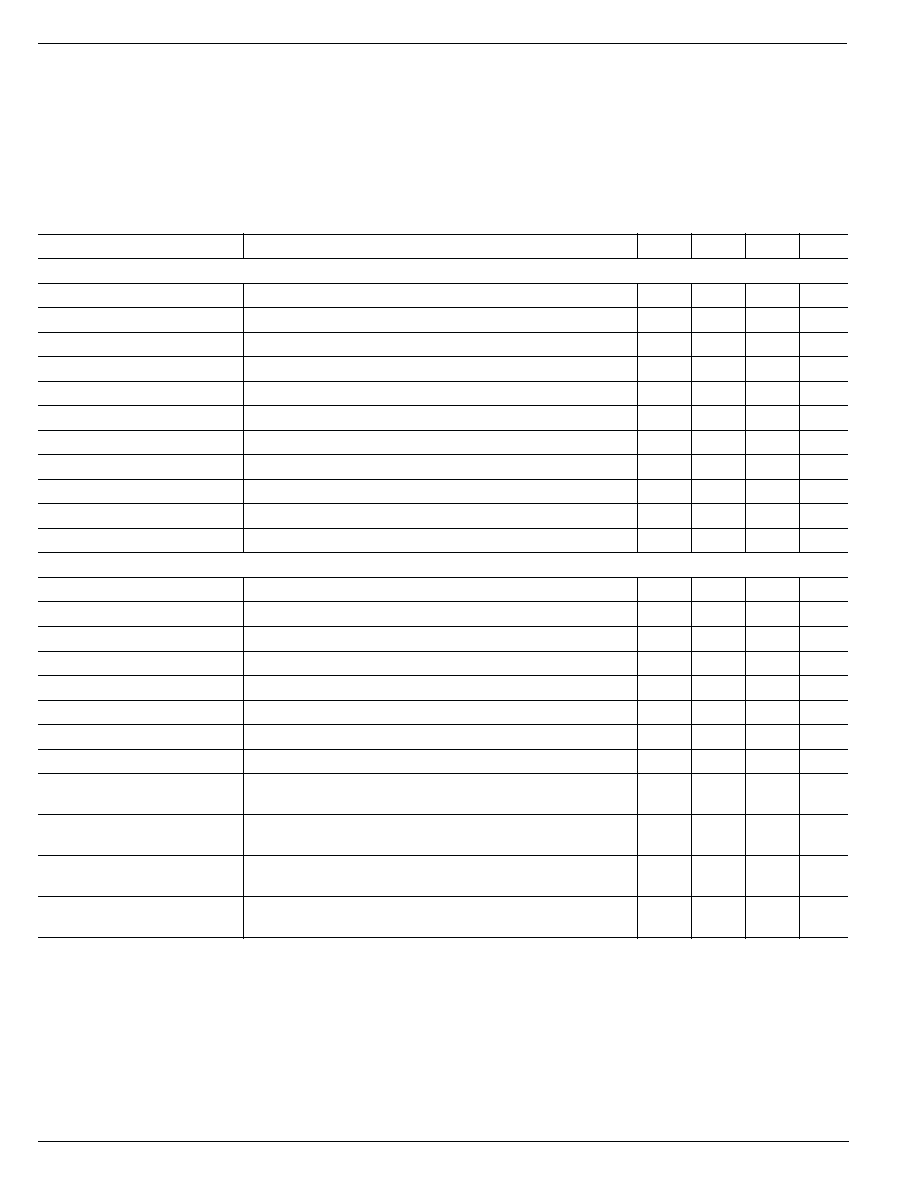
Electrical Characteristics
F
REF
= 850MHz, V
DD
= 2.5 to 3.4V, T
A
= 25
∞C, unless otherwise specified.
Parameter
Condition
Min
Typ
Max
Units
Overall
Operating Frequency
700
850
1100
MHz
Power Down Current
< 1
2
µA
Logic High Input, V
IH
70%
V
DD
Logic Low Input, V
IL
30%
V
DD
DATAIXO, Logic High Output (V
OH
)
I
OH
= ≠500
µA
V
DD
-0.3
V
DATAIXO, Logic Low Output (V
OL
)
I
OL
= 500
µA
0.3
V
LockDet, Logic High Output (V
OH
)
I
OH
= ≠100
µA
V
DD
-0.25
V
LockDet, Logic Low Output (V
OL
)
I
OL
= 100
µA
0.25
V
Clock/Data Frequency
10
MHz
Clock/Data Duty-Cycle
25
75
%
Data Setup to Clock (rising edge)
25
ns
VCO and PLL Section
Prescaler Divide Ratio
64/65
Reference Frequency
40
MHz
PLL Lock Time (int. modulation)
4kHz loop filter bandwidth
1
ms
PLL Lock Time (ext. modulation)
1kHz loop filter bandwidth
4
ms
Rx ≠ (Tx with PA on) Switch Time
1kHz loop filter bandwidth
2.5
ms
Charge Pump Current
±95/±380 ±125/±500 ±155/±620
µA
Transmit Section
f
OUT
= 850MHz
Output Power
R
LOAD
= 50
, V
DD
= 3.0V
10
dBm
Transmit Data Rate (ext. modulation)
Note 4
19.2
128
kbauds
Transmit Data Rate (int. modulation)
Note 5
2.4
kbauds
Frequency Deviation to
Modulation Rate Ratio
unfiltered FSK
1.0
1.5
Current Consumption
Transmit Mode
10 dBm, R
LOAD
= 50
50
mA
Absolute Maximum Ratings
(Note 1)
Maximum Supply Voltage (V
DD
) ................................... +7V
Maximum NPN Reverse Base-Emitter Voltage .......... +2.5V
Storage Temperature Range (T
S
) ............ ≠55
∞C to +150∞C
ESD Rating, Note 3 .................................................... 500V
Operating Ratings
(Note 2)
Supply Voltage (V
IN
) ................................... +2.5V to +3.4V
Ambient Temperature (T
A
) ......................... ≠40
∞C to +85∞C
Package Thermal Resistance
TQFP
(
JA
)-Multilayer board ............................. 46.3
∞C/W

March 2003
5
MICRF500
MICRF500
Micrel
Parameter
Condition
Min
Typ
Max
Units
Receive Section
f
IN
= 850MHz
Receiver Sensitivity (Note 6)
BER=10
-3
≠104
6
dBm
Input 1dB Compression Level
≠34
dBm
Input IP3
≠24
dBm
Input Impedance
22.5-j28.5
W
RSSI Dynamic Range
60
dB
RSSI Output Voltage
P
IN
= ≠100dBm
0.7
V
P
IN
= ≠30dBm
2.1
V
Adjacent Channel Rejection:
f
C
= 10kHz
25kHz channel spacing
26
dB
f
C
= 30kHz
100kHz channel spacing
37
dB
f
C
= 60kHz
200kHz channel spacing
45
dB
f
C
= 200kHz
700kHz channel spacing
48
dB
Blocking Immunity (1MHz)
RC filter: f
C
= 10kHz
66
dB
RC filter: f
C
= 30kHz
61
RC filter: f
C
= 60kHz
59
dB
RC filter: f
C
= 200kHz
53
dB
Maximum Receiver Bandwidth
175
kHz
Receiver Settling Time
1
ms
Current Consumption
gyrator filter f
C
= 60kHz
12
mA
Receive Mode
Current Consumption XCO
300
µA
Note 1.
Exceeding the absolute maximum rating may damage the device.
Note 2.
The device is not guaranteed to function outside its operating rating.
Note 3.
Devices are ESD sensitive. Handling precautions recommended. Human body model, 1.5k in series with 100pF.
Note 4.
Modulation is applied to the VCO and therefore the modulation cannot have any DC component. Some kind of coding is needed to ensure that
the modulation is DC free, e.g., Manchester code or block code. With Manchester code the bitrate is half the baudrate, but with 3B4B block
code the bitrate is
3
/
4
of the baudrate.
Note 5:
Bitrate is the same as the baudrate.
Note 6:
Measured at 19.2k bauds and frequency deviation
±25kHz (external modulation), jitter of received data: < 45%.
-10
-5
0
5
10
15
10 15 20 25 30 35 40 45 50
P
OUT
(dBm)
I
TOT
(mA)
Output Power
vs. Current @ 25
∞C