 | –≠–ª–µ–∫—Ç—Ä–æ–Ω–Ω—ã–π –∫–æ–º–ø–æ–Ω–µ–Ω—Ç: MICRF005 | –°–∫–∞—á–∞—Ç—å:  PDF PDF  ZIP ZIP |

October 2001
1
MICRF005
MICRF005
Micrel
MICRF005
115kbps, 800MHz - 1GHz UHF Receiver
Final Information
General Description
The MICRF005 QwikRadioTM UHF receiver is a single-chip
OOK (on-off keyed) receiver IC for remote wireless applica-
tions. This device is a true single-chip, "antenna-in, data-out"
device. All RF and IF tuning is accomplished automatically
within the IC which eliminates manual tuning production
costs and results in a highly reliable, extremely low-cost
solution for high-volume wireless applications.
The MICRF005 provides two additional key features: (1) A
transmit standby mode, and (2) a shutdown mode which may
be used for duty-cycle operation. These features make the
MICRF005 ideal for low power applications in both one-way
and bi-directional wireless links.
All IF and post-detection (demodulator) data filtering is pro-
vided on the MICRF005, no external filters are required.
Nominal filter bandwidth is fixed a 300kHz allowing a data
throughput at rates up to 115kbps.
Typical Application
SEL0
T/R
VSSRF
REFOSC
VSSRF
NC
ANT
CAGC
VDDRF
NC
VDDBB
SHUT
CTH
DO
VSSBB
C4(CTH)
0.047
µ
F
T/R Control
Y1
14.3359MHz
Data
Output
MICRF005
C1(CAGC)
4.7
µ
F
+5V
915MHz, 115kbps OOK ISM Band Receiver
Features
∑ 800MHz to 1000MHz frequency range
∑ Data rates up to 115kbps
∑ No filters or inductors required
∑ Low 10mA operating supply current at 868MHz
∑ Shutdown mode for >10:1 duty-cycle operation
∑ Very low RF antenna re-radiation
∑ CMOS logic interface for standard ICs
∑ Extremely low external part count
∑ Transmit standby mode for bi-directional link control
Applications
∑ Wireless game controllers
∑ Security systems
∑ Medium-rate data modems
Ordering Information
Part Number
Junction Temp. Range
Package
MICRF005BM
≠40
∞
C to +85
∞
C
14-Lead SOIC
QwikRadio is a trademark of Micrel Semiconductor.
The QwikRadio ICs were developed under a partnership agreement with AIT of Orlando, Florida.
Micrel, Inc. ∑ 1849 Fortune Drive ∑ San Jose, CA 95131 ∑ USA ∑ tel + 1 (408) 944-0800 ∑ fax + 1 (408) 944-0970 ∑ http://www.micrel.com

MICRF005
Micrel
MICRF005
2
October 2001
Pin Configuration
SEL0
T/R
REFOSC
VSSRF
N/C
VSSRF
CAGC
ANT
N/C
VDDRF
SHUT
VDDBB
DO
CTH
VSBB
MICRF005BM
1
14
2
13
3
12
4
11
5
10
6
9
7
8
Standard 14-Pin SOP (M) Package
Pin Description
Pin Number
Pin Name
Pin Function
1
T/R
Transmit/Receive control switch. Pull low to enable receiver function.
2, 3
VSSRF
This pin is the ground return for the RF section of the IC. The bypass
capacitor connected from the VDDRF to VSSRF should have the shortest
possible lead length. For best performance, connect VSSRF to VSSBB at
the power supply only (i.e. keep VSSBB currents from flowing through
VSSRF return paths).
4
ANT
This is the receive RF input, internally ac-coupled. Connect this pin to the
receive antenna. For applications located in high ambient noise environ-
ments, a fixed value band-pass network may be connected between the
ANT pin and VSSRF to provide additional receive selectivity and input
overload protection.
5
VDDRF
This pin is the positive supply input for the RF section of the IC. VDDBB and
VDDRF should be connected together directly at the IC pins.
6
VDDBB
This pin is the positive supply input for the baseband section of the IC.
VDDBB and VDDRF should be connected together at the IC pins.
7
CTH
This capacitor extracts the (DC) average value from the demodulated
waveform which becomes the reference for the internal data slicing com-
parator. Treat as a low-pass RC filter with source impedance of nominally
30k
. A standard
±
20% X7R ceramic capacitor is generally sufficient.
8
VSSBB
This is the ground return for the baseband section of the IC. The bypass and
output capacitors connected to VSSBB should have the shortest possible
leads lengths. For best performance, connect VSSRF to VSSBB at the
power supply only (i.e., keep VSSBB currents from flowing through VSSRF
return path).
9
DO
CMOS-level compatible data output signal.
10
SHUT
Shutdown-mode logic-level control input. Pull low to enable the receiver.
This pin is internally pulled-up to VDDRF.
11
NC
No connection
12
CAGC
Intergrating capacitor for on-chip AGC (Automatic Gain Control). The Decay/
Attack time-constant (TC) ratio is nominally set as 10:1. Use of 0.47
µ
F or
greater is strongly recommended for best range performance. Use low-
leakage type capacitors for duty-cycle operation (Dip Tantalum, Ceramic,
Polyester).
13
NC
No connection
14
REFOSC
This is the timing reference for on-chip tuning and alignment. Connect
crystal between this pin and VSSBB, or drive the input with an AC coupled
0.5V
PP
input clock.

October 2001
3
MICRF005
MICRF005
Micrel
Electrical Characteristics
V
DDRF
= V
DDBB
= V
DD
where 4.75V
V
DD
5.5V, V
SS
= 0V; V
T/R
= V
SHUT
= 0V; C
AGC
= 0.47
µ
F, C
TH
= 4.7nF, 115kbps data-rate (Manchester
encoded); f
REFOSC
= 14.3359MHz (f
RF
= 915MHz); T
A
= 25
∞
C, bold values indicate ≠40
∞
C
T
A
+85
∞
C; current flow into device pins is positive; unless
noted.
Symbol
Parameter
Condition
Min
Typ
Max
Units
I
OP
Operating Current
continuous operation
10
13.5
mA
18.5
10:1 duty cycle
1
mA
I
STBY
Standby Current
V
T/R
= V
SHUT
= V
DD
11
µ
A
RF Section, IF Section
Receiver Sensitivity
Notes 4, 6
≠81
≠84
dBm
f
IF
IF Center Frequency
Note 7
2.496
MHz
f
BW
IF 3dB Bandwidth
Notes 7
1.2
MHz
Maximum Receive Data Rate
115
kb/s
f
ANT
RF Input Range
800
1000
MHz
Receive Modulation Duty-Cycle
20
80
%
Maximum Receiver Input
R
S
= 50
≠10
dBm
Spurious Reverse Isolation
ANT pin, R
SC
= 50
, Note 5
30
µ
Vrms
AGC Attack to Decay Ratio
t
ATTACK
˜
t
DECAY
, Note 9
0.1
AGC Leakage Current
T
A
= +85
∞
C, V
SHUT
= V
DD
or V
T/R
= V
DD
, Note 9
±
200
nA
Reference Oscillator
Synthesizer Stabilization Time
to 1% of final value
1.2
ms
Z
REFOSC
Reference Oscillator
300
k
Input Impedance
OSC Input Voltage
300
mVp-p
Demodulator
Z
CTH
CTH Source Impedance
Note 8, 9
26
k
Z
CTH
CTH Source Impedance Variation
Note 9
±
15
%
Demodulator Filter Bandwidth
Notes 7
300
kHz
Absolute Maximum Ratings
(Note 1)
Supply Voltage (V
DDRF
, V
DDBB
) .................................... +7V
Reference Oscillator Input Voltage (V
REFOSC
) .......... V
DDBB
Input/Output Voltage (V
I/O
) ................. V
SS
≠0.3 to V
DD
+0.3
Junction Temperature (T
J
) ...................................... +150
∞
C
Storage Temperature Range (T
S
) ............ ≠65
∞
C to +150
∞
C
Lead Temperature (soldering, 10 sec.) ................... +260
∞
C
ESD Rating, Note 3
Operating Ratings
(Note 2)
Supply Voltage (V
DDRF
, V
DDBB
) ................ +4.75V to +5.5V
Ambient Temperature (T
A
) ......................... ≠40
∞
C to +85
∞
C

MICRF005
Micrel
MICRF005
4
October 2001
Symbol
Parameter
Condition
Min
Typ
Max
Units
Digital/Control Section
I
IN(pu)
V
SHUT
Pull-Up Current
V
SHUT
= V
SS
8.5
µ
A
I
IN(pd)
V
T/R
Pull-Down Current
V
T/R
= V
DD
12
µ
A
V
IN(high)
V
T/R
,
V
SHUT
, Input-High Voltage
V
DD
≠0.5
V
V
IN(low)
V
T/R
,
V
SHUT
, Input-Low Voltage
0.5
V
I
OUT
Output Current
DO, push-pull
90
µ
A
V
OUT(high)
Output-High Voltage
DO, I
OUT
= ≠5
µ
A
0.9V
DD
V
V
OUT(low)
Output-Low Voltage
DO, I
OUT
= 5
µ
A
0.1V
DD
V
t
R
, t
F
Output Rise and Fall Times
DO, C
LOAD
= 10pF
tbd
µ
s
Note 1.
Exceeding the absolute maximum rating may damage the device.
Note 2.
The device is not guaranteed to function outside its operating rating.
Note 3.
Devices are ESD sensitive. Handling precautions recommended.
Note 4:
Sensitivity is defined as the average signal level measured at the input necessary to achieve 10
-2
BER (bit error rate). The input signal is
defined as a return-to-zero (RZ) waveform with 50% average duty cycle (Manchester encoded data). The RF input is assumed to be matched
into 50
.
Note 5:
Spurious reverse isolation represents the spurious components which appear on the RF input pin (ANT) measured into 50
with an input RF
matching network. Parameter guaranteed by device characterization, not production tested.
Note 6:
Sensitivity, a commonly specified receiver parameter, provides an indication of the receiver's input referred noise, generally input thermal
noise. However, it is possible for a more sensitive receiver to exhibit range performance no better than that of a less sensitive receiver if the
background noise is appreciably higher than the thermal noise. Background noise refers to other interfering signals, such as FM radio stations,
pagers, etc.
A better indicator of achievable receiver range performance is usually given by its selectivity, often stated as intermediate frequency (IF) or
radio frequency (RF) bandwidth, depending on receiver topology. Selectivity is a measure of the rejection by the receiver of "ether" noise.
More selective receivers will almost invariably provide better range. Only when the receiver selectivity is so high that most of the noise on the
receiver input is actually thermal will the receiver demonstrate sensitivity-limited performance.
Note 7:
Parameter scales linearly with reference oscillator frequency f
T
. For any reference oscillator frequency other than 14.3359MHz, compute new
parameter value as the ratio:
f
MHz
14.3359
(parameter value at 14.3359MHz)
REFOSC
◊
Note 8:
Parameter scales inversely with reference oscillator frequency f
T
. For any reference oscillator frequency other than 14.3359MHz, compute
new parameter value as the ratio:
14.3359
f
MHz
(parameter value at 14.3359MHz)
REFOSC
◊
Note 9:
Parameter guaranteed by design (not tested).
Typical Characteristics
0
2
4
6
8
10
12
14
800
820
840
860
880
900
920
940
960
980
1000
CURRENT (mA)
FREQUENCY (MHz)
Supply Current
vs. Frequency
T
A
= 25
∞
C
V
DD
= 5V
0
2
4
6
8
10
12
14
16
-40 -20 0
20 40 60 80 100 120
CURRENT (mA)
TEMPERATURE (
∞
C)
Supply Current
vs. Temperature
f = 915MHz
V
DD
= 5V
October 2001
5
MICRF005
MICRF005
Micrel
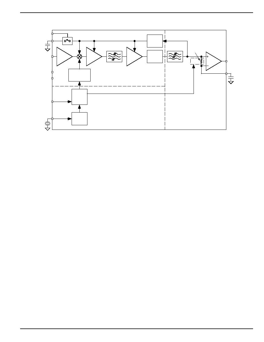
Functional Diagram
Peak
Detector
AGC
Control
2nd Order
Low-Pass Filter
5th Order
Band-Pass Filter
Programmable
Synthesizer
Control
Logic
R
SC
Reference
Oscillator
Crystal
ANT
SHUT
REFOSC
Switched-
Capacitor
Resistor
DO
MICRF005
RF
Amp
IF
Amp
IF
Amp
Compa-
rator
Reference and Control
UHF Downconverter
OOK Demodulator
f
RX
f
LO
f
IF
C
AGC
C
TH
f
T
V
DD
V
SS
C
AGC
T/R
C
TH
MICRF005 Block Diagram
Functional Description
Refer to "MICRF005 Block Diagram". Identified in the block
diagram are the three sections of the IC: UHF Downconverter,
OOK Demodulator and Reference and Control. Also shown
in the figure are two capacitors (C
TH
, C
AGC
) and one timing
component (CR), usually a crystal. With the exception of a
supply decoupling capacitor, these are the only external
components needed by the MICRF005 to construct a com-
plete UHF receiver. Two control inputs are shown in the block
diagram: T/R and SHUT. Through these logic inputs, the user
can control the operation of the IC. These inputs are CMOS
compatible, and are pulled-up on the IC.
IF Bandpass Filter
Rolloff response of the IF Filter is 7th order, while the
demodulator data filter exhibits a 2nd order response.
Slicing Level
Extraction of the dc value of the demodulated signal for
purposes of logic-level data slicing is accomplished using the
external threshold capacitor C
TH
and the on-chip switched-
capacitor "resistor" R
SC
, shown in the block diagram. The
effective resistance of R
SC
is 30k
.
Slicing level time constant values vary somewhat with de-
coder type, data pattern, and data rate, but typical values
range from 5ms to 50ms. Optimization of the value of C
TH
is
required to maximize range.
Squelch
During quiet periods (no signal) the data output (DO pin)
transitions randomly with noise, presenting problems for
some decoders. A simple solution is to introduce a small
offset, or squelch voltage, on the C
TH
pin so that noise does
not trigger the internal comparator. Usually 20mV to 30mV is
sufficient, and may be introduced by connecting a several-
M
resistor from the C
TH
pin to either V
SS
or V
DD
, depending
on the desired offset polarity. Since the MICRF005 has
receiver AGC, noise at the internal comparator input is
always the same, set by the AGC. The squelch offset require-
ment does not change as the local noise strength changes
from installation to installation. Introducing squelch will re-
duce range modestly. Only introduce an amount of offset
sufficient to quiet the output.
Automatic Gain Control
The signal path has AGC (automatic gain control) to increase
input dynamic range. An external capacitor, C
AGC
, must be
connected to the C
AGC
pin of the device. The ratio of decay-
to-attack time-constant is fixed at 10:1 (that is, the attack time
constant is 1/10th of the decay time constant). However, the
attack time constant is set externally by choosing a value for
C
AGC
.
By adding resistance from the C
AGC
pin to V
DDBB
or V
SSBB
in parallel with the AGC capacitor, the ratio of decay-to-attack
time constant may be varied, although the value of such
adjustments must be studied on a per-application basis.
Generally the design value of 10:1 is adequate for the vast
majority of applications.
To maximize system range, it is important to keep the AGC
control voltage ripple low, preferably under 10mVpp once the
control voltage has attained its quiescent value. For this
reason capacitor values of at least 0.47
µ
F are recommended.
The AGC control voltage is carefully managed on-chip to
allow duty-cycle operation of the MICRF005 in excess of
10:1. When the device is placed into shutdown mode (SHUT
pin pulled high), the AGC capacitor floats, to retain the
voltage. When operation is resumed, only the voltage droop
on the capacitor due to leakage must be replenished, there-
fore a relatively low-leakage capacitor is recommended for