 | –≠–ª–µ–∫—Ç—Ä–æ–Ω–Ω—ã–π –∫–æ–º–ø–æ–Ω–µ–Ω—Ç: TH8053 | –°–∫–∞—á–∞—Ç—å:  PDF PDF  ZIP ZIP |
Aug/02
Page 1
3901008053
Rev 004
Baud rate up to 125k Baud
Up to 40 nodes can be connected
Automotive temperature range from -40∞C...125∞C
Very low standby current
Short circuit protection of bus lines to V
DD
, ground and battery
Wake up capability from bus line or wake up pin
Supports unshielded bus wire
Integrated receiver filters
Permanent dominant monitoring of transmit data input
Automatic switching to single wire mode in case of bus failures and automatic reset to differen-
tial mode if bus failure disappeared
One wire transmission mode with ground offset up to 1.5V possible
Very low RFI due internal slope control of bus drivers
Good immunity to EMC
Thermal protection of bus line drivers
Part No.
Temperature Range
Package
TH8053.2
K ( -40∫C to 125∫C )
DC (SOIC14, 150mil)
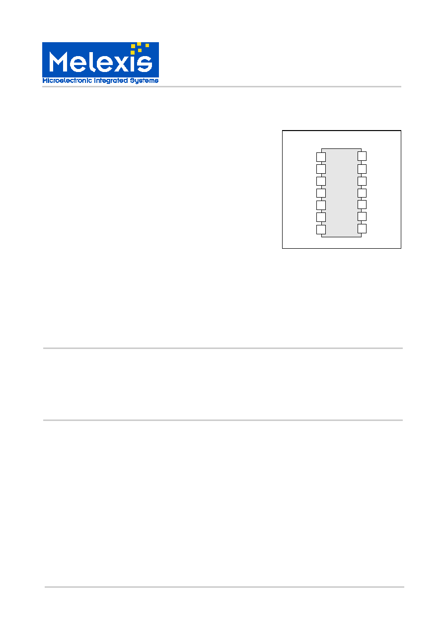
Pin Diagram
TH8053
1
2
3
4
14
13
12
11
INH
VBAT
NERR
RXD
TXD
CANH
CANL
GND
5
6
7
STB
WAKE
EN
10
9
8
RTH
RTL
VDD
SOIC14NB
The TH8053 is a fault tolerant CAN-Transceiver which
works as an interface between the CAN protocol control-
ler and the physical CAN bus. It is designed to connect
up to 40 control nodes in passenger cars with an overall
cable length of up to 80m enabling data trans-mission/
reception rates up to 125
kBaud using unshielded bus
wires.
In normal operation mode the device supports the high
security differential transmit capability of the differential
CAN bus. In the recessive state data coming from the
bus is filtered and after converting to a single-ended sig-
nal fed to the RXD output pin that is to be connected to
the CAN controller (reception of data). In the dominant
state data send from the controller to pin TXD drives the
CAN bus lines.
The device automatically switches to an appropriate sin-
gle ended mode in the case of a bus failure ensuring fur-
ther function of the l network. If the failure gets removed
the TH8053 automatically resets itself to normal opera-
tion. Furthermore it enables single ended transmission
on wires with a ground shift up to 1.5V. The TH8053 also
ensures the data transfer if the system contains a single
TH8053
Fault Tolerant Low Speed CAN Transceiver

TH8053
Fault Tolerant Low Speed CAN Transceiver
Aug/02
Page 2
3901008053
Rev 004
Wake- up
Standby/Sleep
Control
Timer
Temperature
protection
Failure
management
Filter
Receiver
Output
stage
H-
Termination
1
INH
Slope
control
Driver
stage
Output
stage
7
5
6
2
WAKE
STB
EN
TXD
4
NERR
3
RXD
13
GND
RTH
8
CANL
12
11
CANH
9
RTL
10
VDD
14
VBAT
Failure
detection
Wake- up
Time- out
L-Termination
(continued)
unpowered node (e.g. a missing termination resistor).
Another feature added is the monitoring of the TXD-input
to prevent the controller from obstructing the CAN bus by
sending a permanent dominant state. The presence of
any of these errors is indicated by a LOW-signal at the
NERR-pin.
Standby and sleep modes enable low current consump-
tion if no transmit capability is needed or if the supply
voltages drop under a specified level. A wake-up function
recalls the normal operation mode whenever a slope is
detected at the WAKE-Pin or transmission of data on the
bus occurs.
Other important features within passenger cars are the
low RF-interference due to a limitation of rise and fall
slopes as well as the insensitiveness to RF-radiation
achieved by integrated receiver filters.
A thermal shut-down circuit prevents the TH8053 from
any damage caused by increased power consumption of
the CAN output stages while all other parts of the circuit
remain working. Furthermore the TH8053's bus connec-
tions (CANH, CANL) are short-circuit proof to battery and
ground voltage as well as any pin is protected against
ESD-Events.
Figure 1 - Block Diagram

TH8053
Fault Tolerant Low Speed CAN Transceiver
Aug/02
Page 3
3901008053
Rev 004
The signal coming from the differential CAN bus is fed to
a filter stage to inhibit high frequencies that interfere the
bus line from disturbing the evaluation of the incoming
bus data. The cut-off frequency of the filters has to be
regarded as a trade-off between RF-suppression and
propagation delay.
The failure detection circuit determines whether one of
the failures described in Table 1, "CAN bus failures, ex-
ists and indicates a present error as an active LOW at
the NERR output. Furthermore the information of the
kind of failure is given to the failure management block
which takes the appropriate measures to ensure trans-
mission and reception of data. This includes the control
of the correct termination of the CAN bus lines as well as
the choice of the right derivation of the receiver signal
(output to the RXD-pin) from the CANH and CANL in-
puts. The failure management also contains the possibil-
ity to disable one of the driver stages (e.g. in the case of
failure 6 the high side driver and the RTH termination are
disabled to reduce current consumption). During any kind
of single-wire data transfer RF-radiation and RF-
sensitivity are increased.
The failure detection consists of two detection circuits,
one being active in the normal operation mode and the
other one working in the standby and sleep modes. Re-
covery of the failures is done with a certain time-out that
depends on the failure. A wake-up function that detects
incoming dominant signals from the bus is also included.
A wake-up command can also be generated by changing
the logical voltage level at the WAKE-pin. The mode the
TH8053 is running within and whether the INH-pin dis-
ables an external voltage regulator can be controlled by
the EN- and STB-pins as shown in Table 3, "Mode Con-
trol, on page 4 and detailed described in "Operation
Modes" on page 4
Another feature implied in this can transceiver device is
Depending on the occurring error appropriate measures
have to be taken to ensure data transmission and recep-
tion. Table 2, "Error Management", lists the means to
achieve this target in the normal operation mode. The
comparator signal that determines the value of RXD is
given in the second column, the third and fourth ones
contain the information whether either one of the termi-
nations RTH or RTL is switched off to reduce the current
flowing in the termination resistances. The last two col-
umns display if one of the transmitter drivers is deacti-
vated.
If an interrupt of the CANH or CANL wire between two
ECUs is detected (failures 1 and 2) there is no need to
disable the corresponding high or low side driver be-
cause differential transmission towards other ECUs may
still be useful.
______________________________
1
If the termination is switched off, a current of 75µA is supplied at the RTH -or RTL-pin.
2
Low side driver is switched off after two unsuccessful attempts of reaching dominant level.
Table 2 - Error Management
Errors 1 and 3a as well as errors 2 and 4 can't be distinguished
by the receiver.
Error
Output
to RXD
Termination
1
RTH
RTL
CANH
CANL
1
D
on
on
on
on
2
D
on
on
on
on
3
H
on
off
on
off
2
3a
D
on
on
on
on
4
D
on
on
on
on
5
H
on
off
on
off
6
L
off
on
on
on
6a
L
off
on
on
on
7
H
on
off
on
off
Driver
Nr. Failure description
Condition
1
CANL wire interrupted
2
CANH wire interrupted
3
V
BAT
>7.2
3a
V1.8V<V
BAT
<7.2V
4
CANH short-circuited to ground
5
CANL short-circuited to ground
6
CANH short-circuited to battery
supply voltage
V
BAT
>7.2 V
6a
1.8V<V
BAT
<7.2V
7
CANH short-circuited to CANL
CANL short-circuited to battery
supply voltage
Table 1 - CAN bus failures
(Definition in accordance with ISO 11519-2)
(continued)
the time-out circuit at the TXD-Input that prevents occu-
pation of the CAN bus by a long-term dominant signal
sent from the CAN controller. If no failure occurs the
TXD-signal coming from the CAN controller is fed to the
driver stage which includes a limitation of slopes to re-
duce RF-interference caused by radiation on the CAN
bus.
To prevent the chip from a thermal breakdown a tem-
perature protection circuit shuts down the driver stages
which represent the biggest part of the whole power con-
sumption. All other parts remain active thus a reception
of data is still possible. After cooling down and reaching
the low temperature level the transmitter will be enabled
again.

TH8053
Fault Tolerant Low Speed CAN Transceiver
Aug/02
Page 4
3901008053
Rev 004
______________________________
1
Wake-up interrupts are released when the normal operation mode is entered
2
Sleep mode will be entered instead of V
BAT
-standby mode if the go-to-sleep command was applied before. (EN may turn LOW as V
DD
drops
without affecting internal functions because of fail safe functionality.)
3
The "missing V
BAT
" flag will be reset to HIGH when the normal operation mode is entered
The different operation modes can be selected by the
signals provided at the EN- and STB-pins. There are
three operation modes which enable reduced power con-
sumption: the sleep mode, the V
BAT
-standby mode and
the V
DD
-standby mode.
The sleep mode (STB=0, EN=0) is the one with the low-
est power consumption because the whole chip and
even the external voltage regulator get disabled. This
mode can only be reached if an intermediate mode
(STB=0, EN=1) is entered which is interpreted as a "go-
to-sleep"-command. Otherwise the chip switches to the
V
BAT
-standby mode (STB=0, EN=0) where the external
voltage regulator remains further active. In these modes
(go-to-sleep, sleep, V
BAT
-standby) the RTL-pin is
switched to V
BAT
.
If the external inhibitable voltage regulator is not the one
that provides the V
DD
-supply voltage or if the device is
operating in the V
BAT
-standby mode (external voltage
regulator is active) a wake-up request from either the
WAKE-pin or the CAN bus line is visible as an active
LOW at the NERR and RXD outputs. If V
DD
has been
switched off in the sleep mode the wake-up request will
cause the TH8053 to enter the V
BAT
-standby mode as an
intermediate state in which the V
DD
-supply is present
again and so the wake-up can be observed at the NERR-
and RXD-pins as well.
Table 3 -Mode Control
/STB EN
Mode
INH
NERR
RXD
RTL
0
0
V
BAT
-standby
1
high V
BAT
switched to V
BAT
0
0
sleep
2
floating
switched to V
BAT
0
1
go-to-sleep command
floating
switched to V
BAT
1
0
V
DD
-standby
3
high/ V
BAT
active LOW
missing V
BAT
flag
active LOW
wake-up interrupt
switched to V
DD
1
1
normal operation
high/ V
BAT
active LOW
error flag flag
HIGH = recessive bus;
LOW = dominant bus
switched to V
DD
active LOW wake-up interrupt signal if V
DD
is
present
Another mode is the V
DD
-standby mode (STB=1, EN=0).
Similar to the normal operation mode the RTL-pin is
switched to V
DD
. The appearance of a wake-up condition
in this mode is only displayed at the RXD output as an
active LOW. The NERR output is used to indicate the
drop of V
BAT
below 1V. This warn flag is necessary to
show that V
BAT
was missing and that a reinitialisation has
to be done. It is reset to HIGH when the device enters
the normal operation mode in which the NERR-pin is
used to indicate bus failures.
During the low power modes (sleep, V
BAT
- and V
DD
-
standby) the detection of errors is reduced to the moni-
toring of the appearance of failures 5, 6 and 7. A com-
plete deactivation of the detection circuit is not senseful
because the occurrence of failures 5, 6 and 7 would re-
sult in an increased power consumption.
The TH8053 switches itself to the V
BAT
-standby mode if
V
DD
is missing or below the thresh-old. If V
DD
is missing
the EN and STB inputs will be held internally at LOW
level to prevent the chip from entering an inappropriate
mode (fail safe functionality). In all standby modes the
TH8053 is able to receive interrupts. During the first time
of the go-to-sleep command and the specified time after
switching from the normal operation mode to the standby
modes the device ignores an interrupt.
flag that it has to reinitialize the ECU (e.g. after exchang-
ing the complete CAN unit or after a battery voltage
breakdown).
Through entering the normal mode the VBAT low flag will
be reset. Due to special output stages the CAN bus is
not loaded if V BAT = 0V which ensures data transmis-
sion on the CAN bus even if some ECUs are unpowered.
The chip automatically enters the V BAT -standby mode
because of its fail safe functionality. In the V BAT -
standby mode the INH output will become HIGH and
therefore the voltage regulator will provide V
DD
-supply.
The CAN transceiver will remain in the V
BAT
-standby
mode until the CAN controller sets it to another mode.
The controller should first enter V
DD
-standby Mode. This
way the CAN controller will be shown by the power-on

TH8053
Fault Tolerant Low Speed CAN Transceiver
Aug/02
Page 5
3901008053
Rev 004
All voltages are referenced to ground (GND). Positive
currents flow into the IC. The absolute maximum ratings
(in accordance with IEC 134) given in the table below are
limiting values that do not lead to a permanent damage
of the device but exceeding any of these limits may do
Absolute maximum ratings
______________________________
1
t < 500ms; load dump
2
V
DD
=0 to 5.5V; V
BAT
>0 V; t<0.1; no time limit
3
V
DD
=0 to 5.5V; V
BAT
>0 V; t<0.1 ms; load dump
4
For a human body model (equivalent to discharging 100pF with 1.5k
).
5
For a human body model (equivalent to discharging 100pF with 1.5k
).
6
Junction temperature is defined in IEC 747-1
Parameter
Symbol
Min
Max
Unit
Notes
DC supply voltage
V
CC
-0.3
+6.0
V
Battery voltage
V
Bat
-0.3
+27
V
40
1
DC Input voltage at pins 2 to 6
V
2-6
-0.3
V
CC
+ 0.3
V
CANH, CANL input voltage
V
CANH,L
-10
27
V
2
-40
40
3
CANH, CANL transient input voltage
V
CANH, L, tran
-150
100
V
Termination resistance at pins 8 and 9
R
TH,
R
TL
500
16000
DC input voltage at pin 1, 8, 9
V
1,8,9
-0.3
V
BAT
+0.3
V
DC input voltage at pin 7
V
WAKE
V
BAT
+0.3
V
DC input current at pin 7
I
WAKE
-15
mA
Maximum latch-up free current at any pin
I
Latch-up
-500
+500
mA
Electrostatic discharge voltage at any pin
V
ESD
-2000
+2000
V
4
Storage temperature range
T
STG
-55
+150
∞C
Junction temperature
T
Junc
-40
+150
∞C
6
Thermal Resistance from junction to ambient
R
Th
120
K/W
so.Long term exposure to limiting values may affect the
reliability of the device. Reliable operation of the TH8053
is only specified within the limits shown in "Operating
conditions"
Operating Conditions
Parameter
Symbol
Min
Max
Unit
Notes
DC supply voltage
V
DD
4.75
5.25
V
Battery voltage
V
BAT
6
27
V
Operating ambient temperature
T
amb
-40
+125
∞C
Junction temperature
T
junc
-40
+150
∞C
6