 | –≠–ª–µ–∫—Ç—Ä–æ–Ω–Ω—ã–π –∫–æ–º–ø–æ–Ω–µ–Ω—Ç: MLX90124 | –°–∫–∞—á–∞—Ç—å:  PDF PDF  ZIP ZIP |

3901090124
Page 1 of 18
Aug/02
Rev. 001
Features
128bit EEPROM code
125kHz Read/Write Transponder
Same reading range as state of the art Read Only transponders.
EEPROM programmable encoding and data rate options
EEPROM programmable write protection levels
Integrated tuning capacitance
Single command programming with integrity check.
Small die size for ISO-chipcard, without need for tag module.
Available with or without Goldbumps (MEGAPADS)
Applications
Animal ID (ISO 11784/-85 compliant), Access Control, Smart products, Self reconfiguring
equipment, Self calibrating products, Product Authentication, Asset Protection, ... .
Ordering Information
Part No.
Temperature Suffix
Package Code
MLX90124
C (0∞C to 70∞C)
UA
(TO-92)
E (-40∞C to 85∞C) (*)
UF(*)
(Die sawn on blue foil)
UG(*) (Gold bumped Die sawn on blue foil)
UH(*) (Gold bumped Die tape on reel)
UJ (*) (Die tape on reel)
(*) only for large volume requests
Functional Diagram
90124
DUT
Description
The MLX90124 is a 128bit Read Write transponder
operating in the 125kHz range. It has been designed as
a low cost read write solution for applications that do not
require high flexibility in terms of write range.
Requiring only the external coil to be added, it comes
with an 250pF integrated tune capacitor and with a
MEGAPADS option for all established assembly
methods. It is also small enough to be integrated in ISO
smart cards without requiring an expensive transponder
module.
Clock and power supply are taken from the
electromagnetic field. A resistor is switched in parallel to
the parallel resonant LC-circuit to amplitude modulate
the electromagnetic field. The EEPROM is configured as
9 words of 16 bits. Words 1 to 8 form the ID and are
continuously read out during normal operation.
The transponder can be configured for Manchester or
Biphase encoding, at 2 or 4 kBaud by EEPROM
programming the 9
th
word.
By setting 2 other bits in the 9
th
word, the transponder
memory can be either completely locked, or password
protected for limited access. In the first case it becomes
a 128bit Read Only transponder.
Thanks to its low power consumption, and strong
modulation signal, it performs very well in applications
requiring maximum reading distance like animal ISO.

3901090124
Page 2 of 18
Aug/02
Rev. 001
TABLE OF CONTENTS
Features................................................................................................................................................. 1
Applications............................................................................................................................................ 1
Ordering Information............................................................................................................................... 1
1 MLX90124 Electrical Specifications ................................................................................................... 3
2 General Description........................................................................................................................... 5
1.1 Power ON level ........................................................................................................................ 5
1.2 Sensitivity level ........................................................................................................................ 5
1.3 Clock recovery ......................................................................................................................... 5
1.4 Demodulator ............................................................................................................................ 5
1.5 RF limiter, or clamping ............................................................................................................. 5
1.6 Modulator................................................................................................................................. 5
1.7 EEPROM Memory organization................................................................................................ 6
3 OPERATING MODES ....................................................................................................................... 6
1.8 Read Modes ............................................................................................................................ 6
1.8.1
NORMAL READ MODE: .................................................................................................6
1.8.2
CRITICAL READ MODE:.................................................................................................6
1.9 Write Modes (WP=0)................................................................................................................ 7
1.9.1
PROGRAMMING MODE: ................................................................................................7
1.10 Unprotected Write (UW) mode (WP=0,PP=0) ........................................................................... 7
1.10.1 Programming cycle..........................................................................................................7
1.10.2 Purpose of the UW ..........................................................................................................7
1.10.3 Applications of the UW mode:..........................................................................................7
1.11 Password Protected Write (PP) mode (WP=0, PP=1) ............................................................... 8
1.11.1 Compare cycle ................................................................................................................8
1.11.2 Applications of the PP mode:...........................................................................................8
1.12 Read Only (RO) Mode (WP=1, PP=x) ...................................................................................... 8
4 Data encoding schemes .................................................................................................................... 9
1.13 Manchester .............................................................................................................................. 9
1.14 Biphase.................................................................................................................................... 9
5 Timing specification ........................................................................................................................... 9
1.15 Asynchronous Control Pattern (ACP) ....................................................................................... 9
1.16 Start bit (SB) ............................................................................................................................ 9
1.17 Data bits reception ................................................................................................................... 10
1.18 Erase and write phases............................................................................................................ 10
6 Flow Chart......................................................................................................................................... 13
7 FAQ .................................................................................................................................................. 14
8 Unique Features ................................................................................................................................ 15
9 Cross Reference................................................................................................................................ 15
10 Absolute Maximum Ratings ............................................................................................................... 15
11 ESD Precautions ............................................................................................................................... 15
12 Package Information.......................................................................................................................... 15
1.19 Dimensions with MEGAPADS .................................................................................................. 15
1.20 Dimensions without MEGAPADS ............................................................................................. 15
1.21 Blistertape................................................................................................................................ 16
1.22 Pin out flat TO92 (UA) .............................................................................................................. 17
13 Reliability Information ........................................................................................................................ 18
14 Disclaimer ......................................................................................................................................... 18
3901090124
Page 3 of 18
Aug/02
Rev. 001
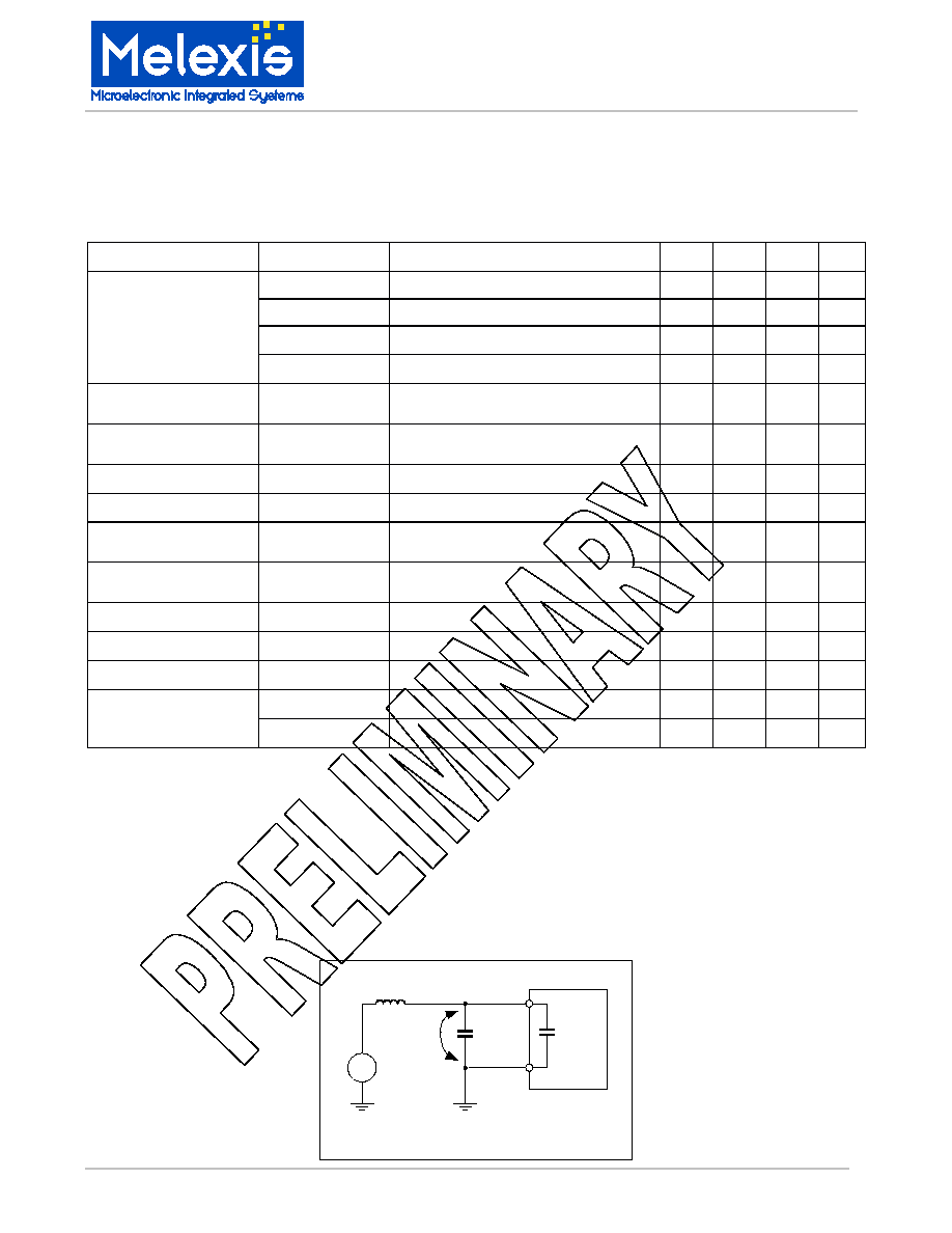
1 MLX90124 Electrical Specifications
Operating Parameters are based on test set up (see Schematic below).
ToperC = 0
∞
C to 70
∞
C, ToperE = -40
∞
C to 85
∞
C (unless otherwise specified)
Parameter
Symbol
Test Conditions
Min
Typ
Max Units
Sensitivity level
Vacsens
Vac, Continuous normal reading of the ID
200 mVpp
Transponder Modulation Depth
VWeakModL
VDUT for Vac = 200mVpp (Weak power)
0.3
0.5 Vpp
VWeakModH
VDUT for Vac = 200mVpp (Weak power)
4.5
5.5
7.5 Vpp (4)
VMedModL
VDUT for Vac = 6Vpp (Medium power)
5.5
7
Vpp
VMedModH
VDUT for Vac = 6Vpp (Medium power)
16
18
Vpp
2kbaud Programming voltage
threshold
Vpr2low
12
15 Vpp
4kbaud Programming voltage
threshold
Vpr4low
12
15 Vpp
EEPROM data retention
Tret
Critical reading ID, Tstore=25
o
C
10
year
EEPROM write cycles
Ncycle
Critical reading ID
100k
cycles
Coil-GND tune capacitor in UA,
UF, UJ delivery forms
Ctune_Trim
Toper=25
o
C, Vdut = 1Vpp
245
250
255 pF (5)
Coil-GND tune capacitor in
bumped die
Ctune_nt_mean
Toper=25
o
C, Vdut = 1Vpp
220
275
330 pF (5)
Intra lot spread
Ctune_nt_spread
Toper=25
o
C, Vdut = 1Vpp
-2.5%
2.5% pF (5)
Dynamic tune capacitor
Ctune_dyn
Toper=25
o
C, Vdut = 6Vpp
6
pF
Toper=25
o
C, Vdut = 10Vpp
10
pF
IclampLow
VdutDC = +/- 2V
40
700 nA
DC input current clamping
IclampHigh
VdutDC = +/- 10V
1
3.5
10 mA
Notes:
Vac
90124
DUT
Vdut
Ctune
COIL
GND
L=6.8mH, Q=80 @120kHz
Cpar=30pF
Note (1): All specification values are tested 100%, or guaranteed by design.
Note (2): All specifications are valid for Manchester and Biphase encoding, and for 2kbaud and 4kbaud data rate options.
Note (3): All ac signals are sinusoidal.
Note (4): VweakModL_Min = minimum voltage on the coil input pins (VDUTmin) at which code is guaranteed to be correct.
Note (5): In UA package the tune capacitor has a fixed mean value with a tight tolerance of +/-2%.
In goldbumped delivery form mean value of the tune capacitor is fixed with a production lot,but can vary +/-20%
between lots. The statistical spread within one lot (+/-50k pcs) is +/-2.5%. For instance range for a mean value
at 275 the tune capacitance values within one production lot are in the range [268: 282]pF.
Temperature shift is typically -0.5% from 25C to -40
∞
C, and +2% at 85
∞
C.

3901090124
Page 4 of 18
Aug/02
Rev. 001
R
F
L
i
m
i
t
e
r
POR
Digital
Controller
EEPROM
M
o
d
u
l
a
t
o
r
ADDR
DATA
COIL
VSS
VDD
CLOCK
RECOVERY
M
O
D
VDD
SUPPLY
VDD
DATA
DEMODUL.
SPEED
CLOCK
Ctune
Cbuffer
EEPROM memory map
BITPOSITION (LSB first)
A
D
D
R
E
S
S
F
U
N
C
T
I
O
N
W
P
=
P
P
=
0
W
P
=
0
,
P
P
=
1
W
P
=
1
0 1 2 3 4 5 6 7 8 9 A B C D E F
0
1
2
3
R
O
4
5
6
7
I
D
R
W
R
O
8
O
p
t
i
o
n
s
R
W
(
R
W
)
-
S
P
E
E
D
C
O
D
E
W
P
P
P
X
X
X
X
X
X
X
X
X
X
X
X
Block diagram

3901090124
Page 5 of 18
Aug/02
Rev. 001
2 General Description
The MLX90124 is a 128bit Read-Write transponder IC for
fixed distance writing. The integrated tune capacitance
and the external coil form a resonant LC antenna that
absorbs part of the electromagnetic energy radiated by
the transceiver LC antenna. Physically, a magnetic
coupling occurs between the transceiver, also referred to
as "reader", and transponder antennas.
To amplitude modulate (AM) the RF carrier, the
transponder damps the electromagnetic field by switching
a resistor in parallel with its coil. This way the transponder
repetitively transmits its 128bit-identification code (ID) to
the transceiver, which recovers the envelope of the
damped field, and decodes the ID.
The transceiver can send commands and data to the
transponder by modulating the amplitude of the carrier.
1.1 Power ON level
When the transponder is placed in an external radio
frequency (RF) field of appropriate frequency and
amplitude, the internal power supply (VDD) can build up
as charge on the integrated buffer capacitance. The
modulation resistor is switched on and off as soon as VDD
has reached the Power On Reset (VPOR) level. When
the modulation resistor is switched on, the tag survives on
the energy stored on its internal capacitance. If
insufficient energy is stored, VDD may drop below VPOR,
at which point the transponder will stop modulating its
code. Hence, just beyond the maximum operating
distance the transponder modulates in a more or less
random way, so the reader can not recover the correct
code.
1.2 Sensitivity level
The minimum electromagnetic force (e.m.f.) needed to
guarantee a correct code transmission is defined by
VDUTmin. At this level the power supply will not drop
below the POR level while the modulation resistance is
switched on during modulation, even for a long series of
short high periods.
1.3 Clock recovery
The transponder takes its clock from the carrier frequency.
Depending on the speed option, the carrier frequency is
divided by 32(4kbaud), 64(2kbaud) to generate the bit
rate.
1.4 Demodulator
If the external RF field is AM modulated according to the
asynchronous control pattern (ACP, see below), the
transponder stops transmitting the 128bit ID and enters
the Program Mode.
The ACP transitions are detected using a fixed threshold
level. This threshold may vary due to process variation
between Min and Max values of the programming level
(Vpr). While the transponder is modulating a sample is
taken each bit period just before the modulation resistor is
switched on.
After the ACP, the transponder synchronizes its sampling
point with the falling edge of the start bit (SB). For each
additional
16bit word
that is
sent,
the
90124
resynchronizes on the SB that has to be sent before the
actual word (see timing specification below).
Note:
The Vpr requirements limit the write distance to typically a
few mm when applied with a small reader coil where the
field varies rapidly over distance. A bigger reader coil
diameter will relax these constraints.
1.5 RF limiter, or clamping
The build up of voltage on the resonant LC circuit is
limited to avoid damaging the internal circuit. This causes
the transponder Q to drop at higher fields.
1.6 Modulator
The modulator consists of a modulation resistor that is
switched in parallel with the resonant LC circuit (antenna).
Because in weak RF fields the rising edge is much slower
than the falling edge of the envelope, a symmetrically
driven modulator would give an asymmetrical envelope.
This is anticipated by delaying each falling edge by a fixed
number of RF clock pulses. Each ON state is reduced by
8 (4) clocks in 2 (4) kBaud mode, and each OFF state is
prolonged by the same amount.
Speed Total clocks
per Bit
Clocks `ON' state
Clocks `OFF' state
2kbaud
64
Long ON = 64 - 8
Short ON = 32 - 8
Long ON = 64 + 8
Short ON = 32 + 8
4kbaud
32
Long ON = 32 ≠ 4
Short ON = 16 ≠ 4
Long ON = 32 + 4
Short ON = 16 + 4