 | –≠–ª–µ–∫—Ç—Ä–æ–Ω–Ω—ã–π –∫–æ–º–ø–æ–Ω–µ–Ω—Ç: MXD1210 | –°–∫–∞—á–∞—Ç—å:  PDF PDF  ZIP ZIP |

For free samples & the latest literature: http://www.maxim-ic.com, or phone 1-800-998-8800
_______________General Description
The MXD1210 nonvolatile RAM controller is a very low-
power CMOS circuit that converts standard (volatile)
CMOS RAM into nonvolatile memory. It also continually
monitors the power supply to provide RAM write protec-
tion when power to the RAM is in a marginal (out-of-
tolerance) condition. When the power supply begins to
fail, the RAM is write protected, and the device switch-
es to battery-backup mode.
Applications
µP Systems
Computers
Embedded Systems
____________________________Features
o
Battery Backup
o
Memory Write Protection
o
230µA Operating-Mode Quiescent Current
o
2nA Backup-Mode Quiescent Current
o
Battery Freshness Seal
o
Optional Redundant Battery
o
Low Forward-Voltage Drop on V
CC
Supply Switch
o
5% or 10% Power-Fail Detection Options
o
Tests Battery Condition During Power-Up
o
8-Pin SO Available
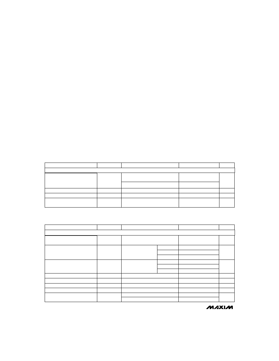
______________Ordering Information
*Contact factory for dice specifications.
MXD1210
Nonvolatile RAM Controller
________________________________________________________________
Maxim Integrated Products
1
V
CCI
FROM
DECODER
CE
1
2
7
6
3
4
5
8
V
CCO
VBATT1
VBATT2
GND
CE
V
CC
CMOS
RAM
MXD1210
+5V
__________Typical Operating Circuit
1
2
3
4
8
7
6
5
VBATT2
CEO
CE
GND
TOL
VBATT1
V
CCO
MXD1210
DIP/SO
16
15
14
13
12
11
10
9
1
2
3
4
5
6
7
8
N.C.
V
CCI
N.C.
VBATT2
VBATT1
N.C.
V
CCO
N.C.
MXD1210
N.C.
CEO
N.C.
CE
GND
N.C.
TOL
N.C.
Wide SO
V
CCI
TOP VIEW
19-0154; Rev 1; 3/96
PART
TEMP. RANGE
PIN-PACKAGE
MXD1210CPA
8 Plastic DIP
MXD1210CSA
8 SO
MXD1210CWE
0∞C to +70∞C
16 Wide SO
0∞C to +70∞C
0∞C to +70∞C
MXD1210C/D
Dice*
MXD1210ESA
-40∞C to +85∞C
8 SO
MXD1210EPA
-40∞C to +85∞C
8 Plastic DIP
MXD1210EWE
-40∞C to +85∞C
16 Wide SO
MXD1210MJA
-55∞C to +125∞C
8 CERDIP
0∞C to +70∞C
_________________Pin Configurations
MXD1210
Nonvolatile RAM Controller
2
_______________________________________________________________________________________
ABSOLUTE MAXIMUM RATINGS
ELECTRICAL CHARACTERISTICS
(T
A
= T
MIN
to T
MAX
, unless otherwise noted.)
Stresses beyond those listed under "Absolute Maximum Ratings" may cause permanent damage to the device. These are stress ratings only, and functional
operation of the device at these or any other conditions beyond those indicated in the operational sections of the specifications is not implied. Exposure to
absolute maximum rating conditions for extended periods may affect device reliability.
ELECTRICAL CHARACTERISTICS
(V
CCI
= +4.75V to +5.5V, TOL = GND; or V
CCI
= +4.5V to +5.5V, TOL = V
CCO
; T
A
= T
MIN
to T
MAX
; unless otherwise noted.)
V
CCI
to GND ................................................................-0.3V, +7V
VBATT1 to GND.......................................................... -0.3V, +7V
VBATT2 to GND.......................................................... -0.3V, +7V
V
CCO
to GND..................................................... -0.3V, V
S
+ 0.3V
(V
S
= greater of V
CCI
, VBATT1, VBATT2)
Digital Input and Output Voltages to GND............. 0.3V, V
CCI
+ 0.3V
Continuous Power Dissipation (T
A
= +70∞C)
8-Pin Plastic DIP (derate 9.09mW/∞C above +70∞C) ....727mW
8-Pin SO (derate 5.88mW/∞C above +70∞C).................471mW
16-Pin Wide SO (derate 9.52mW/∞C above +70∞C)......762mW
8-Pin CERDIP (derate 8.00mW/∞C above +70∞C).........640mW
Operating Temperature Ranges
MXD1210C_ _ ..................................................... 0∞C to +70∞C
MXD1210E_ _ .................................................. -40∞C to +85∞C
MXD1210MJA ................................................ -55∞C to +125∞C
Storage Temperature Range ........................... -65∞C to +150∞C
Lead Temperature (soldering, 10sec) ............................ +300∞C
NORMAL SUPPLY MODE, TOL = V
CCO
mA
0.23
0.5
I
CCI
Supply Current
4.25
4.49
TOL = V
CCO
V
2.4
I
OL
High-Level Output Voltage
µA
±1.0
V
Output Leakage Current
4.50
4.74
V
CCO
,
CEO open,
VBATT1 = VBATT2 = 3V
µA
±1.0
I
IL
Input Leakage Current
80
I
OH
= -1mA
TOL = GND
V
CCTP
V
CCI
Trip Point
V
0.23
75
0.4
I
OL
= 4mA
V
OH
mA
0.23
65
I
CCO
V
OL
Low-Level Output Voltage
UNITS
Output Supply Current
V
CCI
- V
CCO
0.2V
(Note 2)
MIN
TYP
MAX
SYMBOL
CONDITIONS
PARAMETER
RECOMMENDED OPERATING CONDITIONS
TOL = V
CCO
4.50
5.50
2.0
4.0
4.75
5.50
TOL = GND
1 or 2 batteries
CONDITIONS
V
V
CCI
Supply Voltage
V
2.2
V
IH
Input High Voltage
V
0.8
V
IL
Input Low Voltage
V
VBATT1
VBATT2
Battery Voltage (Note 1)
UNITS
MIN
TYP
MAX
SYMBOL
PARAMETER
MXD1210C
MXD1210E
MXD1210M
V
CCI
- 0.20
MXD1210C
V
CCI
- 0.21
V
V
CCI
- 0.25
V
CCO
Output Supply Voltage
I
CCO1
= 80mA
(Note 2)
MXD1210E
MXD1210M

Nonvolatile RAM Controller
ELECTRICAL CHARACTERISTICS
(V
CCI
< VBATT; positive edge rate at VBATT1, VBATT2 > 0.1V/
µ
s, T
A
= T
MIN
to T
MAX
; unless otherwise noted.)
MXD1210
ELECTRICAL CHARACTERISTICS
(T
A
= T
MIN
to T
MAX
, unless otherwise noted.)
_______________________________________________________________________________________
3
V
CC
POWER TIMING CHARACTERISTICS
(V
CCI
= +4.75V to +5.5V, TOL = GND; or V
CCI
= +4.5V to +5.5V, TOL = V
CCO
; T
A
= T
MIN
to T
MAX
; unless otherwise noted.)
TIMING CHARACTERISTICS
(V
CCI
< +4.75V to +5.5V, TOL = GND; or V
CCI
< +4.5V , TOL = V
CCO
; T
A
= T
MIN
to T
MAX
; unless otherwise noted.)
Note 1:
Only one battery input is required. Unused battery inputs must be grounded.
Note 2:
I
CCO1
is the maximum average load current the MXD1210 can supply to the memories.
Note 3:
I
CCO2
is the maximum average load current the MXD1210 can supply to the memories in battery-backup mode.
Note 4:
CEO can sustain leakage current only in battery-backup mode.
Note 5:
Guaranteed by design.
Note 6:
t
CE
max must be met to ensure data integrity on power loss.
2
5
20
V
CC
Slew-Rate Power-Down
µs
10
t
FB
300
t
F
ms
t
REC
Recovery at Power-Up
Tolerance to battery power
To out-of-tolerance condition
µs
0
t
R
V
CC
Slew-Rate Power-Up
µs
1.5
t
CE
CE Pulse Width (Note 6)
UNITS
MIN
TYP
MAX
SYMBOL
CONDITIONS
PARAMETER
ns
5
10
20
t
PD
CE Propagation Delay
MXD1210E
5
10
22
5
10
25
MXD1210C
MXD1210M
ns
0
t
PF
UNITS
CE High to Power-Fail (Note 5)
R
L
= 1k
,
C
L
= 50pF
MIN
TYP
MAX
SYMBOL
CONDITIONS
PARAMETER
pF
7
C
OUT
Output Capacitance
pF
5
C
IN
Input Capacitance
UNITS
MIN
TYP
MAX
SYMBOL
CONDITIONS
PARAMETER
INPUT/OUTPUT CAPACITANCE
(Note 5)
PARAMETER
CONDITIONS
SYMBOL
MIN
TYP
MAX
MXD1210C/E
UNITS
MXD1210M
5
µA
Output open
CEO Output Voltage
V
O
VBATT - 0.2
V
V
CCO
,
CEO open
V
CCI
= 0V
VBATT - V
CCO
0.2V
Quiescent Current (Note 1)
I
BATT
2
100
nA
Output Supply Current (Notes 3, 4)
I
CCO2
300
µA
BATTERY-BACKUP MODE

MXD1210
Nonvolatile RAM Controller
4
_______________________________________________________________________________________
FUNCTION
Ground
Tolerance select pin
4
GND
3
TOL
Backed-up supply to RAM
Battery 1 positive connection
1
8-PIN DIP/SO
V
CCO
2
VBATT1
Chip-enable input
5
CE
Chip-enable output
6
CEO
Battery 2 positive connection
7
VBATT2
5V power supply to chip
8
V
CCI
No connect, not internally connected
≠
N.C.
BATTERY
SELECT
BATTERY
TEST
P
P
VOLTAGE LEVEL
DETECTION
FRESHNESS-
SEAL MODE
CEO
CONTROL
P
P
N
V
CCI
VBATT1
VBATT2
CE
TOL
V
CCO
CEO
GND
GND
MXD1210
PIN
9
11
13
8
6
15
1, 3, 5, 7
10, 12, 14, 16
2
16-PIN WIDE SO
4
NAME
______________________________________________________________Pin Description
Figure 1. Block Diagram
______________ Detailed Description
Main Functions
The MXD1210 executes five main functions to perform
reliable RAM operation and battery backup (see
Typical Operating Circuit and Figure 1):
1. RAM Power-Supply Switch: The switch directs
power to the RAM from the incoming supply or
from the selected battery, whichever is at the
greater voltage. The switch control uses the same
criterion to direct power to MXD1210 internal
circuitry.
2. Power-Failure Detection: The write-protection func-
tion is enabled when a power failure is detected.
The power-failure detection range depends on the
state of the TOL pin as follows:
Power-failure detection is independent of the battery-
backup function and precedes it sequentially as the
power-supply voltage drops during a typical power
failure.
3. Write Protection: This holds the chip-enable output
(
CEO) to within 0.2V of V
CCI
or of the selected bat-
tery, whichever is greater. If the chip-enable input
(
CE )is low (active) when power failure is detected,
then
CEO is held low until CE is brought high, at
which time
CEO is gated high for the duration of
the power failure. The preceding sequence com-
pletes the current RD/WR cycle, preventing data
corruption if the RAM access is a WR cycle.
4. Battery Redundancy: A second battery is optional.
When two batteries are connected, the stronger
battery is selected to provide RAM backup and to
power the MXD1210. The battery-selection circuitry
remains active while in the battery-backup mode,
selecting the stronger battery and isolating the
weaker one. The battery-selection activity is trans-
parent to the user and the system. If only one bat-
tery is connected, the second battery input should
be grounded.
5. Battery-Status Warning: This notifies the system
when the stronger of the two batteries measures
2.0V. Each time the MXD1210 is repowered
(V
CCI
> V
CCTP
) after detecting a power failure, the
battery voltage is measured. If the battery in use is
low, following the MXD1210 recovery period, the
device issues a warning to the system by inhibit-
ing the second memory cycle. The sequence is as
follows:
First access: read memory location n, loc(n) = x
Second access: write memory location n,
loc (n) = complement (x)
Third access: read memory location n, loc (n) = ?
If the third access (read) is complement (x), then the
battery is good; otherwise, the battery is not good.
Return to loc(n) = x following the test sequence.
Freshness-Seal Mode
The freshness-seal mode relates to battery longevity
during storage rather than directly to battery backup.
This mode is activated when the first battery is connect-
ed, and is defeated when the voltage at V
CCI
first
exceeds V
CCTP
. In the freshness-seal mode, both bat-
teries are isolated from the system; that is, no current is
drained from either battery, and the RAM is not pow-
ered by either battery. This means that batteries can be
installed and the system can be held in inventory with-
out battery discharge. The positive edge rate at
VBATT1 and VBATT2 should exceed 0.1V/
µ
s. The bat-
teries will maintain their full shelf-life while installed in
the system.
Battery Backup
The
Typical Operating Circuit shows the MXD1210 con-
nected in order to write protect the RAM when V
CC
is
less than 4.75V, and to provide battery backup to the
supply.
MXD1210
Nonvolatile RAM Controller
_______________________________________________________________________________________
5
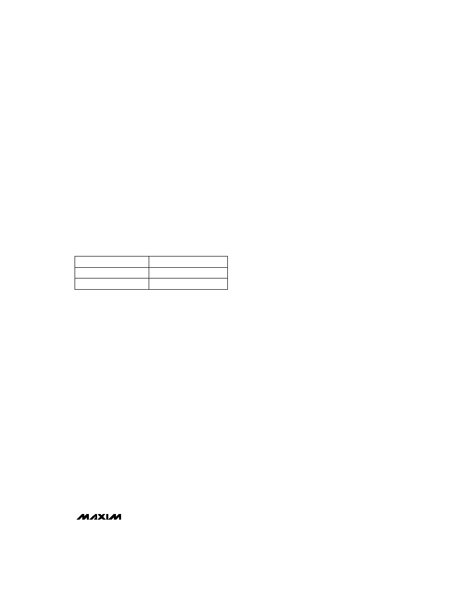
CONDITION
V
CCTP
RANGE (V)
TOL = GND
4.75 to 4.50
TOL = V
CCO
4.50 to 4.25