MAX9981EV
Evaluates: MAX9981
MAX9981 Evaluation Kit
________________________________________________________________ Maxim Integrated Products
1
DESIGNATION
QTY
DESCRIPTION
C1, C4
2
33pF ±5%, 50V C0G
ceramic
capacitors (0603)
Murata GRM1885C1H330J
C2, C3
2
3.9pF ±0.25pF, 50V C0G
ceramic
capacitors (0603)
Murata GRM1885C1H3R9C
C5, C6,
C9, C10
4
100pF ±5%, 50V C0G
ceramic
capacitors (0603)
Murata GRM1885C1H101J
C7, C8
2
15pF ±5%, 50V C0G
ceramic
capacitors (0603)
Murata GRM1885C1H150J
C11, C12
2
0.033µF ±10%, 25V X7R
ceramic
capacitors (0603)
Murata GRM188R71E333K
C13, C16,
C17, C20
4
220pF ±5%, 50V C0G
ceramic
capacitors (0603)
Murata GRM1885C1H221J
C14, C15,
C18, C19
4
330pF ±5%, 50V C0G
ceramic
capacitors (0603)
Murata GRM1885C1H331J
Component List
19-2691; Rev 0; 12/02
For pricing, delivery, and ordering information, please contact Maxim/Dallas Direct! at
1-888-629-4642, or visit Maxim's website at www.maxim-ic.com.
PART
TEMP RANGE
IC PACKAGE
MAX9981EVKIT
-40
°C to +85°C
36 QFN-EP*
(6mm
× 6mm)
SUPPLIER
PHONE
WEBSITE
Coilcraft
800-322-2645 www.coilcraft.com
Digi-Key
800-344-4539 www.digikey.com
Johnson
507-833-8822 www.johnsoncomponents.com
Mini-Circuits
718-934-4500 www.minicircuits.com
Murata
770-436-1300 www.murata.com
Component Suppliers
Ordering Information
*EP = Exposed paddle.
General Description
The MAX9981 evaluation kit (EV kit) simplifies the evalu-
ation of the MAX9981 825MHz to 915MHz dual high-lin-
earity active down-converter mixer. It is fully assembled
and tested at the factory. Standard 50
SMA connec-
tors are included for the inputs and outputs to allow
quick and easy evaluation on the test bench.
This document provides a list of equipment required to
evaluate the device, a straightforward test procedure to
verify functionality, a description of the EV kit circuit,
the circuit schematic, a bill of materials (BOM) and art-
work for each layer of the PC board.
Contact MaximDirect sales at 888-629-4642 to check
on pricing and availability for these kits.
Features
o Fully Assembled and Tested
o +27.3dBm Input IP3
o +13.6dBm Input 1dB Compression Point
o 825MHz to 915MHz RF Frequency
o 725MHz to 1085MHz LO Frequency
o 70MHz to 170MHz IF Frequency
o 2.1dB Conversion Gain
o 10.8dB Noise Figure
o 42dB Channel-to-Channel Isolation
o -5dBm to +5dBm LO Drive
o Built-In LO Switch with 52dB LO1-to-LO2 Isolation
DESIGNATION
QTY
DESCRIPTION
L1L4
4
560nH ±5% wire-wound
inductors (1008)
Coilcraft 1008CS-561XJBC
R1, R2
2
267
±1% resistors (0603)
R3R6
4
137
±1% resistors (0603)
R7
1
47k
±5% resistor (0603)
J1J6
6
PC board edge-mount SMA RF
connectors (flat tab launch)
Johnson 142-0741-856
T1, T2
1
4:1 transformers (200:50)
Mini-Circuits TC4-1W-7A
TP1
1
Large test point for 0.063in PC board
(red) Mouser 151-107
TP2
1
Large test point for 0.063in PC board
(black) Mouser 151-103
TP3
1
Large test point for 0.063in PC board
(white) Mouser 151-101
U1
1
MAX9981EGX-T*
*The exposed paddle conductor on U1 must be solder
attached to a grounded pad on the circuit to ensure a proper
electrical/thermal design.
Evaluates: MAX9981
MAX9981 Evaluation Kit
2
_______________________________________________________________________________________
Quick Start
The MAX9981 EV kit is fully assembled and factory test-
ed. Follow the instructions in the Connections and
Setup section for proper device evaluation.
Test Equipment Required
Table 1 lists the equipment required to verify the opera-
tion of the MAX9981 EV kit. It is intended as a guide
only, and some substitutions can be made.
Connections and Setup
This section provides a step-by-step guide for testing
the basic functionality of the EV kit. As a general pre-
caution to prevent damaging the outputs by driving
high-VSWR loads, do not turn on DC power or RF
signals until all connections are made.
This procedure is specific to operation with an RF input
frequency range of 825MHz to 915MHz, low-side injected
LO for a 100MHz IF. Choose the test frequency based on
the particular system's frequency plan, and adjust the
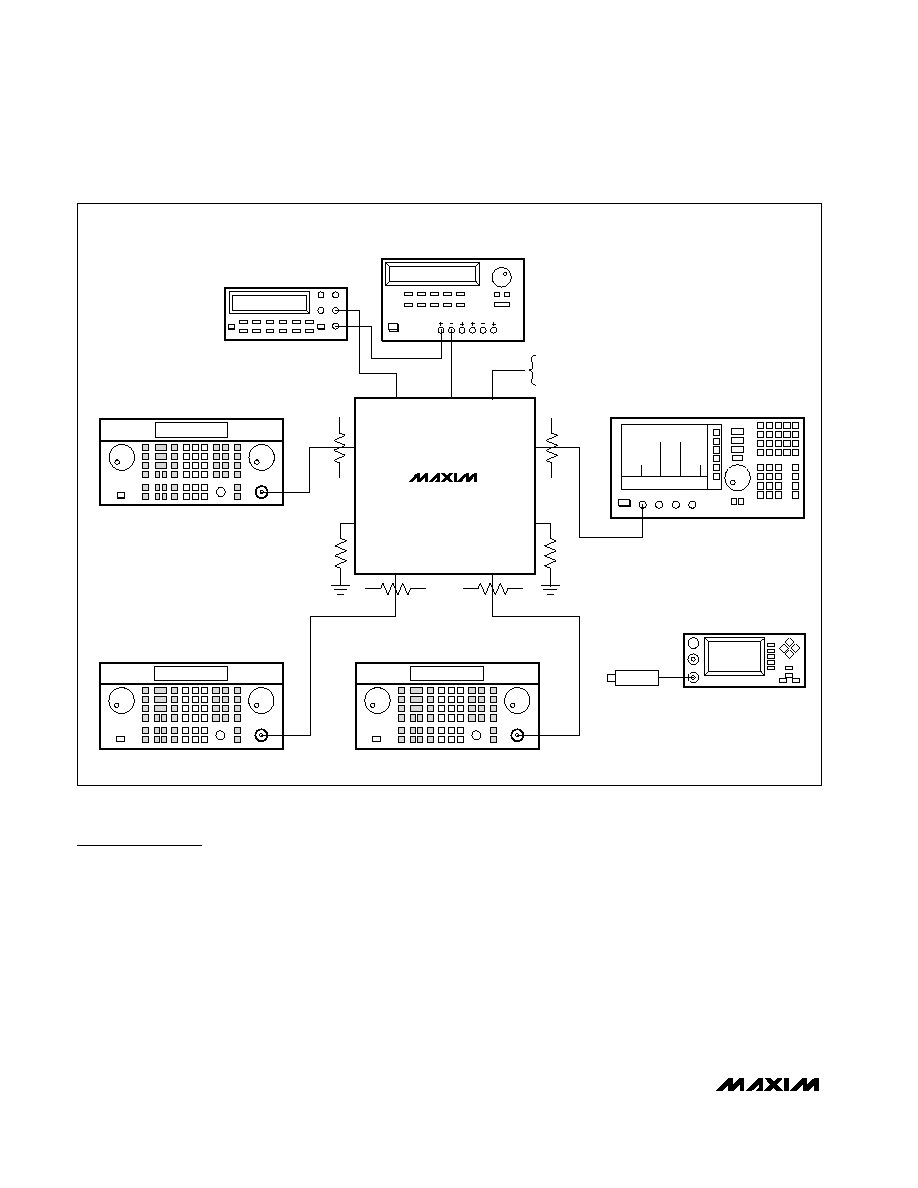
following procedure accordingly. See Figure 1 for the
main mixer test setup diagram.
1) Calibrate the power meter for 870MHz. For safety
margin, use a power sensor rated to at least
+20dBm, or use padding to protect the power head
as necessary.
2) Connect 3dB pads to DUT ends of each of the
three RF signal generators' SMA cables. This
padding improves VSWR and reduces the errors
due to mismatch.
3) Use the power meter to set the RF signal genera-
tors according to the following:
· RFMAIN signal source: -5dBm into DUT at
870MHz (approximately -2dBm before the 3dB
pad)
· LO1 signal source: 0dBm into DUT at 770MHz
(approximately +3dBm before the 3dB pad)
· LO2 signal source: 0dBm into DUT at 771MHz
(approximately +3dBm before the 3dB pad)
4) Disable the signal generator outputs.
5) Connect the RF source (with pad) to RFMAIN.
6) Connect the LO1 and LO2 signal sources to the EV
kit LO inputs.
7) Measure loss in the 3dB pad and the cable that is
connected to IFMAIN. Losses are frequency
dependent, so test this at 100MHz (IF frequency).
Use this loss as an offset in all output power/gain
calculations.
8) Connect this 3dB pad to the EV kit's IFMAIN con-
nector, and connect a cable from the pad to the
spectrum analyzer.
9) Connect a 50
terminator to the unused RF input
and IF output.
10) Set the DC supply to +5.0V, and set a current limit to
around 500mA if possible. Disable the output voltage
and connect supply to the EV kit through a low inter-
nal resistance ammeter. Enable the supply. Re-adjust
the supply to get +5.0V at the EV kit since there will
be a voltage drop across the ammeter when the
mixer is drawing current.
11) Select LO1 by leaving LOSEL (TP3) unconnected
or connecting it to +5V. If left floating, LOSEL will
be pulled high by an on-board pullup resistor.
12) Enable the LO and the RF sources.
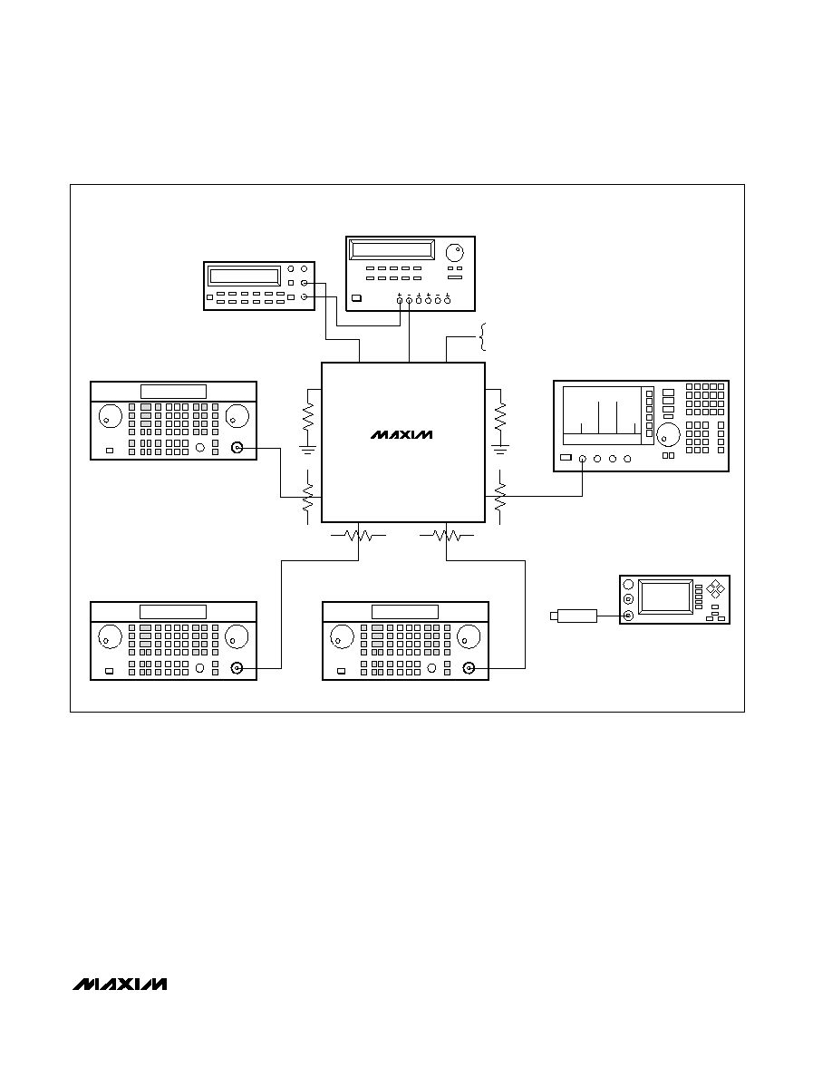
To test the diversity mixer, disable the LO and RF
sources, turn off the DC supply and repeat steps 3
through 12, replacing RFDIV for RFMAIN and IFDIV for
IFMAIN. Be sure to terminate RFMAIN and IFMAIN with
50
terminators. See Figure 2 for diversity mixer test
setup.
Testing the Mixer
Adjust the center and span of the spectrum analyzer to
observe the IF output tone at 100MHz. The level should
be about -5.4dBm (2.6dB conversion gain, 3dB pad
loss). The spectrum analyzer's absolute magnitude
accuracy is typically no better than ±1dB; therefore,
use the power meter to get an accurate output power
measurement. There will also be a tone at 99MHz which
is due to the LO signal applied to LO2. The amount of
suppression between the 100MHz and 99MHz signals
is the switch isolation.
Connect LOSEL to GND to select LO2. Observe that
the IF output level at 99MHz increases while the
100MHz level decreases.
EQUIPMENT
QTY
DESCRIPTION
HP E3631A
1
DC power supply
Fluke 75 series II
1
Digital multimeter (ammeter)
HP/Agilent 8648B
3
RF signal generators
HP 437B
1
RF power meter
HP 8561
1
Spectrum analyzer
HP 8482A
1
High-power sensor (power head)
3dB pad
4
3dB attenuators
50
termination
2
50
(1W) terminations
Table 1. Test Equipment Required

Evaluates: MAX9981
MAX9981 Evaluation Kit
_______________________________________________________________________________________
3
Detailed Description
The MAX9981 is a highly integrated downconverter. RF
and LO baluns are integrated on-chip, as well as an LO
buffer and a SPDT LO input select switch. The EV kit cir-
cuit consists mostly of supply decoupling capacitors and
DC-blocking capacitors, allowing for a simple design-in.
Supply Decoupling Capacitors
Ceramic capacitors C5, C6, C9, and C10 are 100pF
used for high-frequency bypass on the supply. C13
and C17 are 220pF bypass capacitors for IF frequen-
cies. C16 and C20 are used to provide IF ground for
the center tap of T1 and T2. Although called out,
replacing C16 and C20 with a short circuit causes little
to no change in performance.
DC-Blocking Capacitors
The MAX9981 has internal baluns on the RFMAIN,
RFDIV, LO1, and LO2 inputs. These inputs have almost
0
resistance at DC. C1 and C4 are 33pF DC-blocking
capacitors on the RF ports and C7 and C8 are 15pF DC
blocks for the LO ports. C14, C15, C18, and C19 are
used to block DC current from flowing into the trans-
formers along with providing flexibility for matching.
RFBIAS
Bias current for the mixer is set with resistors R1 and
R2 (267
±1%). This value was carefully chosen for
best linearity and lowest supply current through testing
at the factory. Changing this value, or using lower toler-
ance resistors degrades performance.
IF±
The MAX9981 employs a differential IF output to offer
increased IP2 system performance. The IF outputs look
like an open collector with 1.8pF of differential capaci-
tance. Inductors L1L4 are used to resonate out the on-
chip and evaluation board capacitance at the IF
frequency of interest along with providing a low-resis-
tance path for biasing of the IF amplifier. R3R6 pro-
vide a real impedance used to establish the 200
differential impedance. C14, C15, C18, and C19 pro-
vide DC blocking along with adding in the flexibility for
tuning. The 4:1 baluns (T1 and T2) transform the 200
differential impedance to 50
single ended for ease of
measurement. The EV kit IF is matched for operation
over the 70MHz to 100MHz frequency range.
Resistors R3R6 affect the gain of the mixer. For a typi-
cal 2.0dB gain, 137
resistors are used for R3R6.
Higher mixer gain can be realized by increasing R3R6
and retuning L1L4, C14, C15, C18, and C19 for IF
impedance matching. For example, R3 through R6 =
250
, L1 through L4 = 330nH, C14 = C15 = C18 = C19
= 56pF yields a mixer gain of 4.6dB at 70MHz IF with
an IF return loss of 12dB.
As the differential IF outputs are relatively high imped-
ance (200
), they are more susceptible to component
parasitics. It is often good practice to relieve the
ground plane directly underneath large components to
reduce associated shunt-C parasitics.
LOSEL
The EV kit includes a 47k
pullup resistor to allow for
easy selection of the LO port. Providing a ground at
TP3 selects LO2, while leaving TP3 open selects LO1.
To drive TP3 from an external source, follow the limits
called out in the MAX9981 data sheet. Logic voltages
should not be applied to TP3 without the +5V applied.
Doing so can cause the on-chip ESD diodes to conduct
and could damage the part.
Modifying the EV Kit
The RF and LO inputs are broadband matched, so
there is no need to modify the circuit for use anywhere
in the 825MHz to 915MHz RF range (725MHz to
1085MHz LO range).
Retuning for a different IF is as simple as scaling the
values of the IF pullup inductors up or down with fre-
quency. The IF outputs look like an open collector with
3.6pF to ground (1.8pF differential) from the chip. This
capacitance, along with approximately 5.6pF from the
evaluation board, can be resonated out at the frequen-
cy of interest by proper selection of the bias inductor
(L1L4). To determine the inductor value use the follow-
ing equation:
The IF output network is tuned for operation at approxi-
mately 70MHz, so a 560nH inductor is used. For lower
IF frequencies (i.e., larger component values), maintain
the component's Q value at the cost of a larger case
size unless it is unavoidable.
f
L x C
IF
=
1
2
Evaluates: MAX9981
MAX9981 Evaluation Kit
4
_______________________________________________________________________________________
3dB
3dB
LO2
RFMAIN
LO1
+5V
GND
IFMAIN
771.000MHz
RF SIGNAL GENERATOR
(HP 8648B)
770.000MHz
RF SIGNAL GENERATOR
(HP 8648B)
(AMMETER)
291mA
BENCH MULTIMETER
(HP 34401A)
5.0V 500mA (MAX)
POWER SUPPLY
(AG E3631A)
870.000MHz
RF SIGNAL GENERATOR
(HP 8648B)
RF SPECTRUM ANALYZER
(HP 8561x)
RFDIV
IFDIV
RF HIGH-
POWER SENSOR
RF POWER METER
(GIGA 80701A, HP 437B)
50
50
3dB
3dB
LOSEL
OPEN = LO1
GND = LO2
MAX9981
U1
Figure 1. MAX9981 EV Kit Main Mixer Test Setup Diagram
Layout Considerations
The MAX9981 evaluation board can be a guide for your
board layout. Pay close attention to thermal design and
close placement of parts to the IC. The MAX9981 pack-
age exposed paddle (EP), conducts heat from the part
and provides a low-impedance electrical connection.
The EP must be attached to the PC board ground plane
with a low thermal and electrical impedance contact.
Ideally, this can be achieved by soldering the backside
package contact directly to a top metal ground plane on
the PC board. Alternatively, the EP can be connected to
a ground plane using an array of plated vias directly
below the EP.
Depending on the ground plane spacing, large sur-
face-mount pads in the IF path may need to have the
ground plane relieved under them to reduce shunt
capacitance.
Evaluates: MAX9981
MAX9981 Evaluation Kit
_______________________________________________________________________________________
5
3dB
3dB
LO2
RFMAIN
LO1
+5V
GND
IFMAIN
771.000MHz
RF SIGNAL GENERATOR
(HP 8648B)
770.000MHz
RF SIGNAL GENERATOR
(HP 8648B)
(AMMETER)
291mA
BENCH MULTIMETER
(HP 34401A)
5.0V 500mA (MAX)
POWER SUPPLY
(AG E3631A)
870.000MHz
RF SIGNAL GENERATOR
(HP 8648B)
RF SPECTRUM ANALYZER
(HP 8561x)
RFDIV
IFDIV
RF HIGH-
POWER SENSOR
RF POWER METER
(GIGA 80701A, HP 437B)
50
50
3dB
3dB
LOSEL
OPEN = LO1
GND = LO2
MAX9981
U1
Figure 2. MAX9981 EV Kit Diversity Mixer Test Setup Diagram