 | –≠–ª–µ–∫—Ç—Ä–æ–Ω–Ω—ã–π –∫–æ–º–ø–æ–Ω–µ–Ω—Ç: MAX9244 | –°–∫–∞—á–∞—Ç—å:  PDF PDF  ZIP ZIP |
General Description
The MAX9242/MAX9244/MAX9246 deserialize three
LVDS serial-data inputs into 21 single-ended LVCMOS/
LVTTL outputs. A separate parallel-rate LVDS clock pro-
vides the timing for deserialization. The MAX9242/
MAX9244/MAX9246 feature spread-spectrum capability,
allowing the output data and clock frequency to spread
over a specified range to reduce EMI. The single-ended
data and clock outputs are programmable for a frequency
spread of ±2%, ±4%, or no spread. The spread-spectrum
function is also available when the MAX9242/MAX9244/
MAX9246 operate in non-DC-balanced mode. The modu-
lation rate of the spread is 32kHz for a 33MHz LVDS clock
input and scales linearly with frequency. The single-
ended outputs have a separate supply, allowing +1.8V to
+5V output logic levels.
The MAX9242/MAX9244/MAX9246 feature program-
mable DC balance, allowing isolation between a serial-
izer and deserializer using AC-coupling. The MAX9242/
MAX9244/MAX9246 operate with the MAX9209/
MAX9213 serializers and are available with a rising-
edge strobe (MAX9242) or falling-edge strobe
(MAX9244/MAX9246). The LVDS inputs meet ISO
10605 ESD specifications with ±30kV Air-Gap
Discharge and ±6kV Contact Discharge ratings.
The MAX9242/MAX9244/MAX9246 are available in a
48-pin TSSOP package and operate over the -40∞C to
+85∞C temperature range.
Applications
Automotive Navigation Systems
Automotive DVD Entertainment Systems
Digital Copiers
Laser Printers
Features
Programmable ±4%, ±2%, or OFF Spread-Spectrum
Output for Reduced EMI
Programmable DC-Balanced or Non-DC-Balanced
Modes
DC Balance Allows AC-Coupling for Wider Input
Common-Mode Voltage Range
Spread Spectrum Operates in DC-Balanced or
Non-DC-Balanced Mode
/ 4 Deskew by Oversampling (MAX9242/MAX9244)
16MHz-to-34MHz (DC-Balanced) and 20MHz-to-
40MHz (Non-DC-Balanced) Operation
(MAX9242/MAX9244)
6MHz-to-18MHz (DC-Balanced) and 8MHz-to-20MHz
(Non-DC-Balanced) Operation (MAX9246)
Rising-Edge (MAX9242) or Falling-Edge
(MAX9244/MAX9246) Output Strobe
High-Impedance Outputs when PWRDWN is Low
Allow Output Busing
Fail-Safe Inputs in Non-DC-Balanced Mode
Separate Output Supply Allows Interface to +1.8V,
+2.5V, +3.3V, and +5V Logic
LVDS Inputs Meet ISO 10605 ESD Protection at
±30kV Air-Gap Discharge and ±6kV Contact
Discharge
LVDS Inputs Meet IEC 61000-4-2 Level 4 ESD
Protection at ±15kV Air-Gap Discharge and ±8kV
Contact Discharge
LVDS Inputs Conform to ANSI TIA/EIA-644 Standard
+3.3V Main Power Supply
MAX9242/MAX9244/MAX9246
21-Bit Deserializers with Programmable
Spread Spectrum and DC Balance
________________________________________________________________ Maxim Integrated Products
1
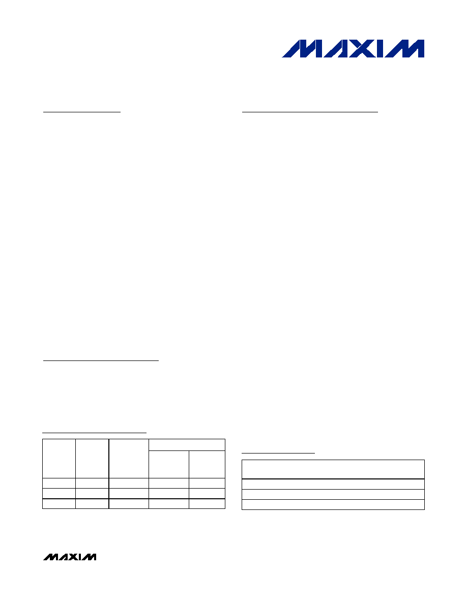
Ordering Information
19-3954; Rev 0; 1/06
For pricing, delivery, and ordering information, please contact Maxim/Dallas Direct! at
1-888-629-4642, or visit Maxim's website at www.maxim-ic.com.
PART
TEMP RANGE
PIN-PACKAGE
PKG
CODE
MAX9242EUM
-40∞C to +85∞C
48 TSSOP
U48-1
MAX9244EUM
-40∞C to +85∞C
48 TSSOP
U48-1
MAX9246EUM
-40∞C to +85∞C
48 TSSOP
U48-1
Devices are available in lead-free packaging. Specify lead free by
adding a + symbol at the end of the part number when ordering.
Selector Guide
FREQUENCY RANGE
PART
STROBE
EDGE
OVER-
SAMPLING
NON-DC
BALANCE
(MHz)
DC
BALANCE
(MHz)
MAX9242
Rising
Yes
20 to 40
16 to 34
MAX9244
Falling
Yes
20 to 40
16 to 34
MAX9246
Falling
No
8 to 20
6 to 18
Pin Configuration appears at end of data sheet.

MAX9242/MAX9244/MAX9246
21-Bit Deserializers with Programmable
Spread Spectrum and DC Balance
2
_______________________________________________________________________________________
ABSOLUTE MAXIMUM RATINGS
DC ELECTRICAL CHARACTERISTICS
(V
CC
= LVDSV
CC
= PLLV
CC
= +3.0V to +3.6V, V
CCO
= +3.0V to +5.5V, PWRDWN = high; SSG = high, open, or low; DCB = high or
low, differential input voltage |V
ID
| = 0.05V to 1.2V, input common-mode voltage V
CM
= |V
ID
/ 2| to 2.4V - |V
ID
/ 2|, unless otherwise
noted. Typical values are at V
CC
= V
CCO
= LVDSV
CC
= PLLV
CC
= +3.3V, |V
ID
| = 0.2V, V
CM
= +1.25V, T
A
= +25∞C.) (Notes 1, 2)
Stresses beyond those listed under "Absolute Maximum Ratings" may cause permanent damage to the device. These are stress ratings only, and functional
operation of the device at these or any other conditions beyond those indicated in the operational sections of the specifications is not implied. Exposure to
absolute maximum rating conditions for extended periods may affect device reliability.
(All voltages referenced to GND.)
V
CC
, LVDSV
CC
, PLLV
CC
.......................................-0.5V to +4.0V
V
CCO
......................................................................-0.5V to +6.0V
RxIN_, RxCLKIN_ ..................................................-0.5V to +4.0V
PWRDWN ..............................................................-0.5V to +6.0V
SSG, DCB...................................................-0.5V to (V
CC
+ 0.5V)
RxOUT_, RxCLKOUT ...............................-0.5V to (V
CCO
+ 0.5V)
Continuous Power Dissipation (T
A
= +70∞C)
48-Pin TSSOP (derate 16mW/∞C above +70∞C) ........1282mW
ESD Protection
Human Body Model (R
D
= 1.5k
, C
S
= 100pF)
All Pins to GND .............................................................±2.5kV
IEC 61000-4-2 (R
D
= 330
, C
S
= 150pF)
LVDS Inputs to GND (Air-Gap Discharge).....................±15kV
LVDS Inputs to GND (Contact Discharge).......................±8kV
ISO 10605 (R
D
= 2.0k
, C
S
= 330pF)
LVDS Inputs to GND (Air-Gap Discharge).....................±30kV
LVDS Inputs to GND (Contact Discharge).......................±6kV
Operating Temperature Range ...........................-40∞C to +85∞C
Storage Temperature Range .............................-65∞C to +150∞C
Junction Temperature ......................................................+150∞C
Lead Temperature (soldering, 10s) .................................+300∞C
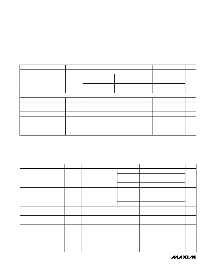
PARAMETER
SYMBOL
CONDITIONS
MIN
TYP
MAX
UNITS
POWER SUPPLY
Power-Supply Range
V
CC
,
LVDSV
CC
,
PLLV
CC
3.0
3.6
V
Output-Supply Range
V
CCO
1.8
5.5
V
16MHz
45
61
DC-balanced
mode (SSG = low)
34MHz
72
96
20MHz
59
79
33MHz
80
106
Non-DC-balanced
mode (SSG = low)
40MHz
93
123
16MHz
57
78
D C - b al anced m od e
( S SG = hi g h or op en) 34MHz
93
125
20MHz
71
96
33MHz
98
129
Worst-Case Supply Current
I
CCW
C
L
= 8pF,
worst-case pattern,
V
CC
= V
CCO
= 3.0V
to 3.6V, Figure 2
(MAX9242,
MAX9244)
N on- D C -b al anced
m ode
( S SG = hi g h or op en) 40MHz
115
145
mA

MAX9242/MAX9244/MAX9246
21-Bit Deserializers with Programmable
Spread Spectrum and DC Balance
_______________________________________________________________________________________
3
DC ELECTRICAL CHARACTERISTICS (continued)
(V
CC
= LVDSV
CC
= PLLV
CC
= +3.0V to +3.6V, V
CCO
= +3.0V to +5.5V, PWRDWN = high; SSG = high, open, or low; DCB = high or
low, differential input voltage |V
ID
| = 0.05V to 1.2V, input common-mode voltage V
CM
= |V
ID
/ 2| to 2.4V - |V
ID
/ 2|, unless otherwise
noted. Typical values are at V
CC
= V
CCO
= LVDSV
CC
= PLLV
CC
= +3.3V, |V
ID
| = 0.2V, V
CM
= +1.25V, T
A
= +25∞C.) (Notes 1, 2)
PARAMETER
SYMBOL
CONDITIONS
MIN
TYP
MAX
UNITS
6MHz
27
41
8MHz
30
45
DC-balanced
mode (SSG = low)
18MHz
43
61
8MHz
33
47
10MHz
37
52
Non-DC-balanced
mode (SSG = low)
20MHz
52
73
6MHz
32
47
8MHz
38
57
D C -b al anced m od e
( S SG = hi g h or op en)
18MHz
57
81
8MHz
41
58
10MHz
46
65
Worst-Case Supply Current
I
CCW
C
L
= 8pF,
worst-case pattern,
V
CC
= V
CCO
= 3.0V
to 3.6V, Figure 2
(MAX9246)
N on- D C -b al anced
m ode
( S SG = hi g h or op en) 20MHz
66
92
mA
Power-Down Supply Current
I
CCZ
PWRDWN = low
50
µA
5V-TOLERANT LOGIC INPUT (PWRDWN)
High-Level Input Voltage
V
IH
2.0
5.5
V
Low-Level Input Voltage
V
IL
-0.3
+0.8
V
Input Current
I
IN
PWRDWN = high or low level
-20
+20
µA
Input Clamp Voltage
V
CL
I
CL
= -18mA
-1.5
V
THREE-LEVEL LOGIC INPUTS (DCB, SSG)
High-Level Input Voltage
V
IH
2.5
V
CC
+
0.3
V
Mid-Level Input Current
I
IM
D C B, S S G op en or connected to a d r i ver w i th
outp ut i n hi g h- i m p ed ance state ( N ote 3)
-10
+10
µA
Low-Level Input Voltage
V
IL
-0.3
+0.8
V
Input Current
I
IN
DCB, SSG = high or low level,
PWRDWN = high or low
-20
+20
µA
Input Clamp Voltage
V
CL
I
CL
= -18mA
-1.5
V
SINGLE-ENDED OUTPUTS (RxOUT_, RxCLKOUT)
I
OH
= -100µA
V
CCO
- 0.1
RxCLKOUT (Note 4)
V
CCO
- 0.25
High-Level Output Voltage
V
OH
I
OH
= -2mA
RxOUT_
V
CCO
- 0.43
V
I
OL
= 100µA
0.1
RxCLKOUT (Note 4)
0.2
Low-Level Output Voltage
V
OL
I
OL
= 2mA
RxOUT_
0.26
V
MAX9242/MAX9244/MAX9246
21-Bit Deserializers with Programmable
Spread Spectrum and DC Balance
4
_______________________________________________________________________________________
AC ELECTRICAL CHARACTERISTICS
(V
CC
= LVDSV
CC
= PLLV
CC
= +3.0V to +3.6V, V
CCO
= +3.0V to +3.6V, C
L
= 8pF, PWRDWN = high; SSG = high, open, or low;
DCB = high or low, differential input voltage |V
ID
| = 0.1V to 1.2V, input common-mode voltage V
CM
= |V
ID
/ 2| to 2.4V - |V
ID
/ 2|, unless
otherwise noted. Typical values are at V
CC
= V
CCO
= LVDSV
CC
= PLLV
CC
= +3.3V, |V
ID
| = 0.2V, V
CM
= +1.25V, T
A
= +25∞C.) (Notes 6, 7, 8)
PARAMETER
SYMBOL
CONDITIONS
MIN
TYP
MAX
UNITS
RxOUT_
2.9
4.7
6.5
Output Rise Time
CLHT
0.1 x V
C C O
to 0.9 x V
C C O
,
Fi g ur e 3
RxCLKOUT
2.0
3.3
4.1
ns
RxOUT_
2.1
3.0
4.2
Output Fall Time
CHLT
0.9 x V
C C O
to 0.1 x V
C C O
,
Fi g ur e 3
RxCLKOUT
1.10
1.94
2.70
ns
16MHz
2560
3142
DC-balanced mode,
Figure 4
34MHz
900
1386
20MHz
2500
3164
RxIN Skew Margin (Note 9)
RSKM
Non-DC-balanced mode,
Figure 4
40MHz
960
1371
ps
RxCLKOUT High Time
RCOH
Figures 5a, 5b
0.35 x
RCOP
ns
RxCLKOUT Low Time
RCOL
Figures 5a, 5b
0.35 x
RCOP
ns
RxOUT Setup to RxCLKOUT
RSRC
Figures 5a, 5b
0.3 x
RCOP
ns
RxOUT Hold from RxCLKOUT
RHRC
Figures 5a, 5b
0.45 x
RCOP
ns
RxCLKIN to RxCLKOUT Delay
RCCD
SSG = low, Figures 6a, 6b
4.5 +
(RCIP / 2)
6.5 +
(RCIP / 2)
8.2 +
(RCIP / 2)
ns
DC ELECTRICAL CHARACTERISTICS (continued)
(V
CC
= LVDSV
CC
= PLLV
CC
= +3.0V to +3.6V, V
CCO
= +3.0V to +5.5V, PWRDWN = high; SSG = high, open, or low; DCB = high or
low, differential input voltage |V
ID
| = 0.05V to 1.2V, input common-mode voltage V
CM
= |V
ID
/ 2| to 2.4V - |V
ID
/ 2|, unless otherwise
noted. Typical values are at V
CC
= V
CCO
= LVDSV
CC
= PLLV
CC
= +3.3V, |V
ID
| = 0.2V, V
CM
= +1.25V, T
A
= +25∞C.) (Notes 1, 2)
PARAMETER
SYMBOL
CONDITIONS
MIN
TYP
MAX
UNITS
High-Impedance Output Current
I
OZ
PWRDWN = low, V
OUT
= -0.3V to (V
CCO
+ 0.3V)
-30
+30
µA
RxCLKOUT (Note 4)
-10
-40
V
CCO
= 3.0V to 3.6V,
V
OUT
= 0V
RxOUT_
-5
-20
RxCLKOUT (Note 4)
-28
-75
Output Short-Circuit Current
(Note 5)
I
OS
VCCO = 4.5V to 5.5V,
VOUT = 0V
RxOUT_
-13
-37
mA
LVDS INPUTS (RxIN_, RxCLKIN_)
Differential Input High Threshold
V
TH
(Note 6)
50
mV
Differential Input Low Threshold
V
TL
(Note 6)
-50
mV
Input Current
I
IN+
, I
IN-
PWRDWN = high or low
-25
+25
µA
Power-Off Input Current
I
INO+
, I
INO-
V
CC
= V
CCO
= 0V or open
-40
+40
µA
Input Resistor 1
R
IN1
PWRDWN = high or low, V
CC
= V
CCO
= 0V or
open, Figure 1
42
78
k
Input Resistor 2
R
IN2
PWRDWN = high or low, V
CC
= V
CCO
= 0V or
open, Figure 1
246
410
k

MAX9242/MAX9244/MAX9246
21-Bit Deserializers with Programmable
Spread Spectrum and DC Balance
_______________________________________________________________________________________
5
Note 1: Current into a pin is defined as positive. Current out of a pin is defined as negative. All voltages are referenced to ground,
except V
TH
and V
TL
.
Note 2: Maximum and minimum limits over temperature are guaranteed by design and characterization. Devices are production
tested at T
A
= +25∞C.
Note 3: To provide a mid level, leave the input open, or, if driven, put driver in high impedance. High-impedance leakage current
must be less than ±10µA.
Note 4: RxCLKOUT limits are scaled based on RxOUT_ measurements, design, and characterization data.
Note 5: One output shorted at a time. Current out of the pin.
Note 6: V
TH
, V
TL
, and AC parameters are guaranteed by design and characterization, and are not production tested. Limits are set
at ±6 sigma.
Note 7: C
L
includes probe and test jig capacitance.
Note 8: RCIP is the period of RxCLKIN. RCOP is the period of RxCLKOUT.
Note 9: RSKM is measured with less than 150ps cycle-to-cycle jitter on RxCLKIN.
AC ELECTRICAL CHARACTERISTICS (continued)
(V
CC
= LVDSV
CC
= PLLV
CC
= +3.0V to +3.6V, V
CCO
= +3.0V to +3.6V, C
L
= 8pF, PWRDWN = high; SSG = high, open, or low;
DCB = high or low, differential input voltage |V
ID
| = 0.1V to 1.2V, input common-mode voltage V
CM
= |V
ID
/ 2| to 2.4V - |V
ID
/ 2|, unless
otherwise noted. Typical values are at V
CC
= V
CCO
= LVDSV
CC
= PLLV
CC
= +3.3V, |V
ID
| = 0.2V, V
CM
= +1.25V, T
A
= +25∞C.) (Notes 6, 7, 8)
PARAMETER
SYMBOL
CONDITIONS
MIN
TYP
MAX
UNITS
Deserializer Phase-Locked-
Loop Set
RPLLS
Figure 7
65,600 x
RCIP
ns
Deserializer Power-Down Delay
RPDD
Figure 8
100
ns
Deserializer Phase-Locked-
Loop Set from SSG Change
RPLLS2
Figure 9
32,800 x
RCIP
ns
M axi m um outp ut
fr eq uency
f
RxCLKIN
+ 3.6%
f
RxCLKIN
+ 4.0%
f
RxCLKIN
+ 4.4%
SSG = high,
Figure 10
Minimum output
frequency
f
RxCLKIN
- 4.4%
f
RxCLKIN
- 4.0%
f
RxCLKIN
- 3.6%
M axi m um outp ut
fr eq uency
f
RxCLKIN
+ 1.8%
f
RxCLKIN
+ 2.0%
f
RxCLKIN
+ 2.2%
SSG = open,
Figure 10
Minimum output
frequency
f
RxCLKIN
- 2.2%
f
RxCLKIN
- 2.0%
f
RxCLKIN
- 1.8%
Spread-Spectrum Output
Frequency
f
RxCLKOUT
SSG = low
f
RxCLKIN
f
RxCLKIN
MHz
Spread-Spectrum Modulation
Frequency
f
SSM
Figure 10
f
RxCLKIN
/
1016
Hz