 | ÐлекÑÑоннÑй компоненÑ: MAX8069 | СкаÑаÑÑ:  PDF PDF  ZIP ZIP |
MAX8069 DS
General Description
The MAX8069 is a 1.2V temperature-compensated volt-
age reference. It uses the bandgap principle to achieve
excellent stability and low noise at reverse currents down
to 60µA. The MAX8069 also features excellent stability,
freedom from oscillation. The MAX8069 is a functional
alternative to Maxim's ICL8069 with an identical pinout.
Applications
Analog-to-Digital Converters
Digital-to-Analog Converters
Threshold Detectors
Voltage Regulators
Portable Instruments
Features
Temperature Coefficient Guaranteed
to 25ppm/°C (max)
Low Bias Current: 60
µ
A (min)
Low Dynamic Impedance
Low Reverse Voltage
Low Cost
MAX8069
Low-Voltage Reference
________________________________________________________________ Maxim Integrated Products
1
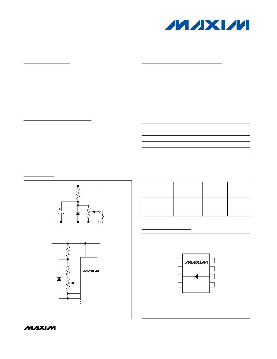
ANODE
N.C.
N.C.
1
+
2
8
7
N.C.
N.C.
N.C.
CATHODE
N.C.
SO
TOP VIEW
3
4
6
5
MAX8069
4.7µF
6.8k
V
OUT
10k
+5V
+5V
REF HI
1k
10k
MAX8069
2.2k
V
+
COMMON
REF LO
MAX8069
*SEE NOTE 2
(a) Simple Reference (1.2V or Less)
(b) Double-Regulated 100mV Reference for ICL7107
One-Chip DPM Circuit
ICL7107
Typical Operating Circuit
19-0618; Rev 0; 7/06
Pin Configurations
Ordering Information
For pricing, delivery, and ordering information, please contact Maxim/Dallas Direct! at
1-888-629-4642, or visit Maxim's website at www.maxim-ic.com.
PART
TEMP RANGE
PIN-
PACKAGE
PKG
CODE
MAX8069ESA+
-40°C to +85°C
8 SO
S8-2
MAX8069CEZQ*
-40°C to +85°C
TO-92
C92-2
MAX8069CCZQ
0°C to +70°C
TO-92
C92-2
Selector Guide
PART
TEMP RANGE
PIN-
PACKAGE
MAX
TEMPCO
(ppm/°C)
MAX8069ESA+
-40°C to +85°C
8 SO
25
MAX8069CEZQ* -40°C to +85°C
TO-92
50
MAX8069CCZQ
0°C to +70°C
TO-92
50
Pin Configurations continued at end of data sheet.
+Denotes lead-free package.
*Future product--contact factory for availability.
MAX8069
Low-Voltage Reference
2
_______________________________________________________________________________________
ABSOLUTE MAXIMUM RATINGS
ELECTRICAL CHARACTERISTICS
(T
A
= +25°C, unless otherwise noted.) (Note 2)
Stresses beyond those listed under "Absolute Maximum Ratings" may cause permanent damage to the device. These are stress ratings only, and functional
operation of the device at these or any other conditions beyond those indicated in the operational sections of the specifications is not implied. Exposure to
absolute maximum rating conditions for extended periods may affect device reliability.
Note 2: If circuit strays in excess of 200pF are anticipated, a 4.7µF shunt capacitor will ensure stability under all operating condi-
tions.
Reverse Voltage ..............................................................(Note 1)
Forward Current ..................................................................10mA
Reverse Current ..................................................................10mA
Power Dissipation.......Limited by Max Forward/Reverse Current
Storage Temperature Range .............................-65°C to +150°C
Operating Temperature Range
MAX8069CCZQ ...................................................0°C to +70°C
MAX8069CEZQ, MAX8069ESA ........................-40°C to +85°C
Lead Temperature (soldering, 10s) .................................+300°C
Note 1: In normal use, the reverse voltage cannot exceed the reference voltage. However, when plugging units into a powered-up
test fixture, an instantaneous voltage equal to the compliance of the test circuit will be seen. This should not exceed 20V.
PARAMETER
CONDITIONS
MIN
TYP
MAX
UNITS
Output Voltage
I
R
= 500µA
1.20
1.22
1.25
V
MAX8069ESA
25
Output Voltage Temperature Coefficient
I
R
= 500µA,
T
A
= T
MIN
to T
MAX
MAX8069C_ZQ
50
ppm/°C
Output Voltage Change
60µA
I
R
5mA
15
20
mV
I
R
= 60µA
1
2
Reverse Dynamic Impedance
I
R
= 500µA
0.6
2
Forward Voltage Drop
I
R
= 500µA
0.6
1
V
RMS Noise Voltage
10Hz
f 10kHz, I
R
= 500µA
20
µV
Reverse Current Range
0.6
5.0
mA
MAX8069
Low-Voltage Reference
_______________________________________________________________________________________
3
REVERSE VOLTAGE
vs. REVERSE CURRENT
MAX8069 toc01
REVERSE CURRENT (µA)
REVERSE VOLTAGE (V)
1000
1.219
1.220
1.221
1.222
1.223
1.224
1.218
10
100
10,000
T
A
= -40°C
T
A
= +25°C
T
A
= +85°C
REVERSE VOLTAGE
vs. REVERSE CURRENT
MAX8069 toc02
REVERSE CURRENT (µA)
REVERSE VOLTAGE (V)
1000
0.9
1.0
1.1
1.2
1.3
1.4
0.8
10
100
10,000
T
A
= -40°C
T
A
= +25°C
T
A
= +85°C
REVERSE VOLTAGE
vs. TEMPERATURE
MAX8069 toc03
TEMPERATURE (°C)
REVERSE VOLTAGE (V)
60
35
10
-15
1.219
1.220
1.221
1.222
1.223
1.224
1.218
-40
85
Typical Operating Characteristics
(T
A
= +25°C, unless otherwise noted.)
BOTTOM VIEW
TO-92
PLASTIC
2
1
ANODE
CATHODE
Pin Configurations (continued)
MAX8069
Low-Voltage Reference
Maxim cannot assume responsibility for use of any circuitry other than circuitry entirely embodied in a Maxim product. No circuit patent licenses are
implied. Maxim reserves the right to change the circuitry and specifications without notice at any time.
4
_____________________Maxim Integrated Products, 120 San Gabriel Drive, Sunnyvale, CA 94086 408-737-7600
© 2006 Maxim Integrated Products
is a registered trademark of Maxim Integrated Products, Inc.
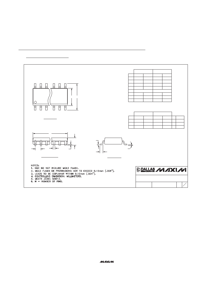
SOICN .EPS
PACKAGE OUTLINE, .150" SOIC
1
1
21-0041
B
REV.
DOCUMENT CONTROL NO.
APPROVAL
PROPRIETARY INFORMATION
TITLE:
TOP VIEW
FRONT VIEW
MAX
0.010
0.069
0.019
0.157
0.010
INCHES
0.150
0.007
E
C
DIM
0.014
0.004
B
A1
MIN
0.053
A
0.19
3.80
4.00
0.25
MILLIMETERS
0.10
0.35
1.35
MIN
0.49
0.25
MAX
1.75
0.050
0.016
L
0.40
1.27
0.394
0.386
D
D
MIN
DIM
D
INCHES
MAX
9.80
10.00
MILLIMETERS
MIN
MAX
16
AC
0.337
0.344
AB
8.75
8.55
14
0.189
0.197
AA
5.00
4.80
8
N MS012
N
SIDE VIEW
H
0.244
0.228
5.80
6.20
e
0.050 BSC
1.27 BSC
C
H
E
e
B
A1
A
D
0-8
L
1
VARIATIONS:
Package Information
(The package drawing(s) in this data sheet may not reflect the most current specifications. For the latest package outline information,
go to
www.maxim-ic.com/packages
.)