 | ÐлекÑÑоннÑй компоненÑ: MAX685ETG | СкаÑаÑÑ:  PDF PDF  ZIP ZIP |
MAX685 DS
For pricing delivery, and ordering information please contact Maxim/Dallas Direct! at
1-888-629-4642, or visit Maxim's website at www.maxim-ic.com.
General Description
The MAX685 DC-DC converter provides low-noise dual
outputs for powering CCD imaging devices and LCDs.
This device uses a single inductor to provide indepen-
dently regulated positive and negative outputs.
Integrated power switches are included in a small 24-
Pin 4mm x 4mm Thin QFN package to save space and
reduce cost. A 16-pin QSOP package is also available.
Each output delivers up to 10mA from a +2.7V to +5.5V
input voltage range. Output voltages are set indepen-
dently up to 24V and down to -9V. With a few additional
low-cost components, the output voltages can be set at
up to 45V and down to -16V. Output ripple magnitude is
30mVp-p. The MAX685 uses a fixed-frequency, pulse-
width-modulated (PWM) control scheme at 220kHz or
400kHz to permit output noise filtering and to reduce
the size of external components. The frequency can
also be synchronized to an external clock signal
between 200kHz and 480kHz.
The MAX685 has a power-OK indicator output (POK)
that signals when both outputs are within regulation. A
logic-controlled shutdown completely turns off both out-
puts and reduces supply current to 0.1µA. The user
can also set which output turns on first.
The preassembled MAX685 evaluation kit is available to
reduce design time.
Applications
Camcorders
LCDs
Digital Cameras
CCD Imaging Devices
Notebooks
Features
o Dual Output Using a Single Inductor
o Low-Noise Output, 30mVp-p Ripple
o Output Voltages up to 24V and down to -9V
(up to 45V and down to -16V with added
components)
o Internal Switches in a Small 24-Pin 4mm x 4mm
Thin QFN Package
o 220kHz/400kHz Fixed-Frequency PWM Operation
o Frequency Can Be Synchronized to External
Clock
o Power-OK Indicator
o Selectable Power-On Sequencing
o 0.1µA Logic-Controlled Shutdown
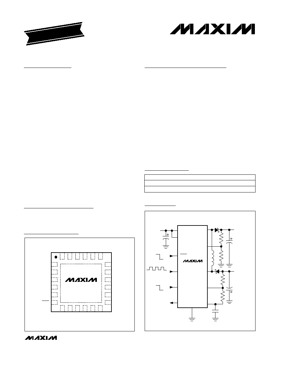
MAX685
Dual-Output (Positive and Negative),
DC-DC Converter for CCD and LCD
________________________________________________________________ Maxim Integrated Products
1
MAX685
VP
V
DD
ON
OFF
INPUT
2.7V TO 5.5V
LXN
FBP
LXP
FBN
REF
GND
NEGATIVE
OUTPUT
DOWN TO -9V,
10mA
POSITIVE
OUTPUT
UP TO 24V,
10mA
SHDN
SYNC
SEQ
POK
POS
NEG
OPTIONAL
POWER-OK
INDICATOR
24
23
22
21
20
19
7
8
9
10
11
12
13
14
15
16
17
18
6
5
4
3
2
1
MAX685
24-TQFN (4mm x 4mm)
TOP VIEW
N.C.
VP
VP
POK
SEQ
SHDN
I.C.
LXP
LXP
LXN
LXN
I.C.
N.C.
PGND
PGND
PGND
FBP
REF
FBN
GND
N.C.
N.C.
V
DD
SYNC
Typical Operating Circuit
19-1353; Rev 1; 6/03
PART
MAX685EEE
-40°C to +85°C
TEMP RANGE
PIN-PACKAGE
16 QSOP
EVALUATION KIT MANUAL
FOLLOWS DATA SHEET
Pin Configuration
Ordering Information
MAX685ETG
-40°C to +85°C
24 TQFN
MAX685
Dual-Output (Positive and Negative),
DC-DC Converter for CCD and LCD
2
_______________________________________________________________________________________
ABSOLUTE MAXIMUM RATINGS
ELECTRICAL CHARACTERISTICS
(V
DD
= VP = 5V, T
A
= 0°C to +85°C unless otherwise noted. Typical values are at T
A
= +25°C.)
Stresses beyond those listed under "Absolute Maximum Ratings" may cause permanent damage to the device. These are stress ratings only, and functional
operation of the device at these or any other conditions beyond those indicated in the operational sections of the specifications is not implied. Exposure to
absolute maximum rating conditions for extended periods may affect device reliability.
V
DD
, VP to GND........................................................-0.3V to +6V
PGND to GND .......................................................-0.3V to +0.3V
V
DD
to VP...............................................................-0.3V to +0.3V
LXN, POK to GND ..................................................-0.3V to +30V
LXP to V
DD
..............................................................-15V to +0.3V
REF, SEQ, SHDN to GND...........................-0.3V to (V
DD
+ 0.3V)
FBP, FBN, SYNC to GND .........................................-0.3V to +6V
Continuous Power Dissipation (T
A
= +70°C)
16-Pin QSOP (derate 8.3mW/°C above +70°C)............667mW
24-Pin TQFN (derate 20.8mW/°C above +70°C) ........1667mW
Operating Temperature Range ...........................-40°C to +85°C
Junction Temperature ......................................................+150°C
Storage Temperature Range .............................-65°C to +165°C
Lead Temperature (soldering, 10s) .................................+300°C
2.7V < V
DD
< 5.5V
2.7V < V
DD
< 5.5V
V
DD
= 5.5V (Note 1)
No load
V
DD
= VP
No load
C3 = C4 = 10µF, I
LOAD
= 5mA
I
OUT
= 0 to 10mA, C1 = 10µF
V
DD
= rising
V
DD
= 4.5V to 5.5V
V
FBP
= 1.35V, V
FBN
= -0.1V
V
DD
= 4.5V, V
OUT+
14.25V, V
OUT-
-7.125V,
Figure 3
T
A
= +25°C
V
DD
= 4.5V
SYNC = SEQ = SHDN = GND
SYNC = V
DD
CONDITIONS
µA
0.1
1
Input Bias Current
V
0.7 x V
DD
Logic-High Input
V
0.3 x V
DD
Logic-Low Input
µA
±0.01
±0.1
FBP, FBN Input Leakage Current
mV
-16
10
36
FBN Threshold Voltage
V
1.21
1.24
1.27
FBP Threshold Voltage
mV
50
UVLO Hysteresis
V
2.35
2.5
2.65
UVLO Threshold
µA
0.1
10
Shutdown Supply Current
V
-9
-1.27
Negative Output Voltage Range
V
VP
24
V
2.7
5.5
Input Voltage Range
Positive Output Voltage Range
mVp-p
30
Output Voltage Ripple
%/mA
0.13
Load Regulation
%/V
0.2
Line Regulation
µA
300
500
Idle Quiescent Current
mA
10
Output Current
mA
440
LX Current Limit
0.6
2
LXP, LXN On-Resistance
mA
0.8
Quiescent Current
UNITS
MIN
TYP
MAX
PARAMETER
0 < I
REF
< 50µA
No load
mV
-2
V
REF
Load Regulation
V
1.23
1.250
1.27
V
REF
Output Voltage
SHUTDOWN (SHDN)
UNDERVOLTAGE LOCKOUT
REFERENCE VOLTAGE
FB INPUTS
LOGIC INPUTS (SEQ, SHDN, SYNC)
MAX685
Dual-Output (Positive and Negative),
DC-DC Converter for CCD and LCD
_______________________________________________________________________________________
3
ELECTRICAL CHARACTERISTICS (continued)
(V
DD
= VP = 5V, T
A
= 0°C to +85°C unless otherwise noted. Typical values are at T
A
= +25°C.)
ELECTRICAL CHARACTERISTICS
(V
DD
, VP = 5V, T
A
= -40°C to +85°C unless otherwise noted.) (Note 2)
Note 1: Negative output voltage can be larger magnitude for lower values of V
DD
. The voltage between V
DD
and V
OUT-
must not
exceed 14.5V.
Note 2: Specifications to -40°C are guaranteed by design, not production tested.
V
DD
= 5.5V (Note 1)
V
DD
= VP
No load
V
DD
= rising
V
IN
= 4.5V, V
OUT+
14.25V, V
OUT-
-7.125V,
Figure 3
SYNC = GND
SYNC = SEQ = SHDN = GND
CONDITIONS
V
-9
-1.27
Negative Output Voltage Range
V
VP
24
V
2.7
5.5
Input Voltage Range
Positive Output Voltage Range
V
1.205
1.275
FBP Threshold Voltage
V
2.35
2.65
UVLO Threshold
mA
10
Maximum Output Current
µA
500
Idle Quiescent Current
µA
10
Shutdown Supply Current
UNITS
MIN
MAX
PARAMETER
CONDITIONS
SYNC = V
DD
SYNC = GND
kHz
320
400
480
Oscillator Frequency (internal)
175
220
265
kHz
200
480
Sync Frequency Range (external)
I
POK
= 2mA
FBN falling
FBP rising
V
0.4
POK Output Low Voltage
mV
UNITS
MIN
TYP
MAX
54
79
108
PARAMETER
FBN POK Threshold
V
1.090
1.122
1.150
FBP POK Threshold
V
POK
= 10V
µA
1
POK Output Off Current
2.7V < V
DD
5.5V
No load
V
0.3 x V
DD
Logic-Low Input
mV
-20
40
FBN Threshold Voltage
2.7V < V
DD
5.5V
V
0.7 x V
DD
Logic-High Input
FBP rising
V
1.090
1.150
FBP POK Threshold
FBN falling
mV
54
108
FBN POK Threshold
SYNC INPUT
POK COMPARATORS
No load
V
1.225
1.275
VREF Output Voltage
SHUTDOWN
UNDERVOLTAGE LOCKOUT
FB INPUTS AND REFERENCE VOLTAGE
LOGIC INPUTS (SEQ, SHDN, SYNC)
POK COMPARATORS
1.240
1.242
1.244
1.248
1.246
1.250
1.252
1.254
-40
20
0
-20
40
60
80
100
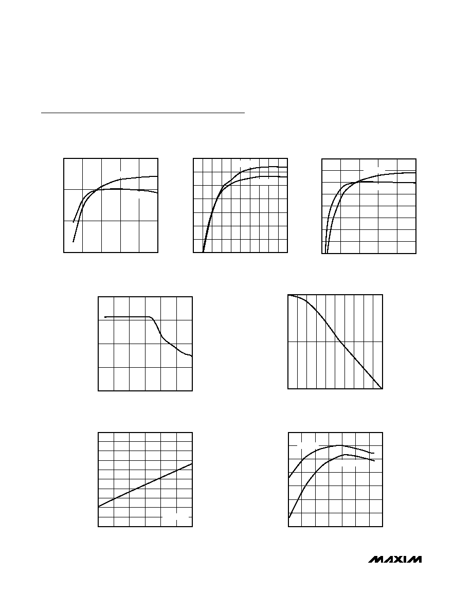
REFERENCE VOLTAGE
vs. TEMPERATURE
MAX685-13
TEMPERATURE (°C)
REFERENCE VOLTAGE (V)
V
IN
= 5.0V
V
IN
= 3.3V
MAX685
Dual-Output (Positive and Negative),
DC-DC Converter for CCD and LCD
4
_______________________________________________________________________________________
60
70
80
90
0
4
2
6
8
10
EFFICIENCY vs. LOAD CURRENT
(POSITIVE OUTPUT LOADED)
MAX685-01
LOAD CURRENT (mA)
EFFICIENCY (%)
V
IN
= 5.0V
V
IN
= 3.3V
50
60
55
70
65
80
75
85
0
4
2
3
5
1
6
7
9
8
10
EFFICIENCY vs. LOAD CURRENT
(NEGATIVE OUTPUT LOADED)
MAX685-02
LOAD CURRENT (mA)
EFFICIENCY (%)
V
IN
= 5.0V
V
IN
= 3.3V
50
65
55
60
75
70
85
80
90
0
4
2
6
8
10
EFFICIENCY vs. LOAD CURRENT
(BOTH OUTPUTS LOADED)
MAX685-03
LOAD CURRENT (mA)
EFFICIENCY (%)
V
IN
= 5.0V
V
IN
= 3.3V
0
0.5
1.0
1.5
2.0
2.5
3.5
3.0
4.0
4.5
5.0
5.5
NO-LOAD CURRENT vs.
INPUT VOLTAGE
MAX685-04
INPUT VOLTAGE (V)
NO-LOAD CURRENT (mA)
150
180
170
160
190
200
210
220
230
240
250
2.7
3.7
3.2
4.2
4.7
5.2
5.7
LX SWITCHING FREQUENCY
vs. INPUT VOLTAGE
MAX865-07
INPUT VOLTAGE (V)
OSCILLATOR FREQUENCY (kHz)
SYNC = V
DD
1.248
1.249
1.250
0
15 20
5
10
25 30
35 40 45
50
REFERENCE LOAD REGULATION
MAX685-06
LOAD CURRENT (µA)
REFERENCE VOLTAGE (V)
Typical Operating Characteristics
(Circuit of Figure 3, V
OUT+
= 15V, V
OUT-
= -7.5V, T
A
= +25°C, unless otherwise noted.)
MAX685
Dual-Output (Positive and Negative),
DC-DC Converter for CCD and LCD
_______________________________________________________________________________________
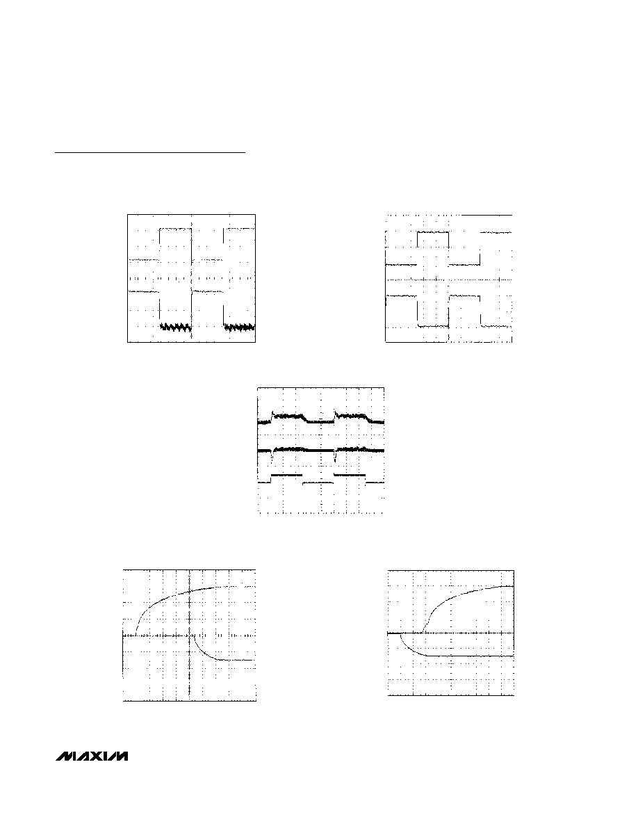
5
11mA
5mA/div
100mV/div
1mA
I
OUT+
V
OUT+
2ms/div
V
OUT+
LOAD-TRANSIENT RESPONSE
MAX685-08
-1mA
5mA/div
100mV/div
-11mA
I
OUT-
V
OUT-
2ms/div
V
OUT-
LOAD-TRANSIENT RESPONSE
MAX685-09
100mV/div
V
OUT+
V
OUT-
V
DD
, VP
2V/div
100mV/div
1ms/div
INPUT 4V TO 5V, +15V AT 10mA, -7.5V AT 10mA
LINE-TRANSIENT RESPONSE
MAX685-10
5V/div
V
OUT+
V
OUT-
5V/div
2ms/div
START-UP, SEQ = LOW, V
DD
= VP = 5.0V,
+15V AT 10mA, -7.5V AT 10mA
START-UP (SEQ = LOW)
MAX685-11
5V/div
V
OUT+
V
OUT-
5V/div
2ms/div
START-UP, SEQ = HIGH, V
DD
= VP = 5.0V,
+15V AT 10mA, -7.5V AT 10mA
START-UP (SEQ = HIGH)
MAX685-12
Typical Operating Characteristics (continued)
(Circuit of Figure 3, V
OUT+
= 15V, V
OUT-
= -7.5V, T
A
= +25°C, unless otherwise noted.)