 | ÐлекÑÑоннÑй компоненÑ: MAX679C/D | СкаÑаÑÑ:  PDF PDF  ZIP ZIP |
/home/web/htmldatasheet/html/maxim/180049
_______________General Description
The MAX679 step-up, regulated charge pump gener-
ates a 3.3V ±4% output voltage from a 1.8V to 3.6V
input voltage (two alkaline, NiCd, or NiMH; or one
Lithium-Ion battery). Output current is 20mA (min) from
a 2.0V input. Only three external capacitors are needed
to build a complete DC-DC converter.
The MAX679's switching frequency is pin selectable at
330kHz or 1MHz to allow trade-offs between lowest
supply current and smallest-size capacitors. The logic
shutdown function reduces the supply current to 5µA
(max) and disconnects the load from the input. Special
soft-start circuitry prevents excessive current from
being drawn from the battery during start-up. This DC-
DC converter requires no inductors and has low EMI. It
is available in the ultra-small µMAX package, which is
only 1.11mm high and half the area of an 8-pin SO.
________________________Applications
Battery-Powered Applications
Miniature Equipment
Backup-Battery Boost Converters
Translators
Two-Way Pagers
____________________________Features
o
Regulated 3.3V ±4% Output
o
Ultra-Small:
1.1mm-High, 8-Pin µMAX Package
o
No Inductors Required
o
Up to 1MHz Operation
(small external components)
o
Fits into 0.05 in.
2
o
Up to 85% Efficiency
o
1.8V to 3.6V Input Voltage Range
o
50µA Quiescent Supply Current
o
1µA Shutdown Current
MAX679
Regulated 3.3V Charge Pump
________________________________________________________________
Maxim Integrated Products
1
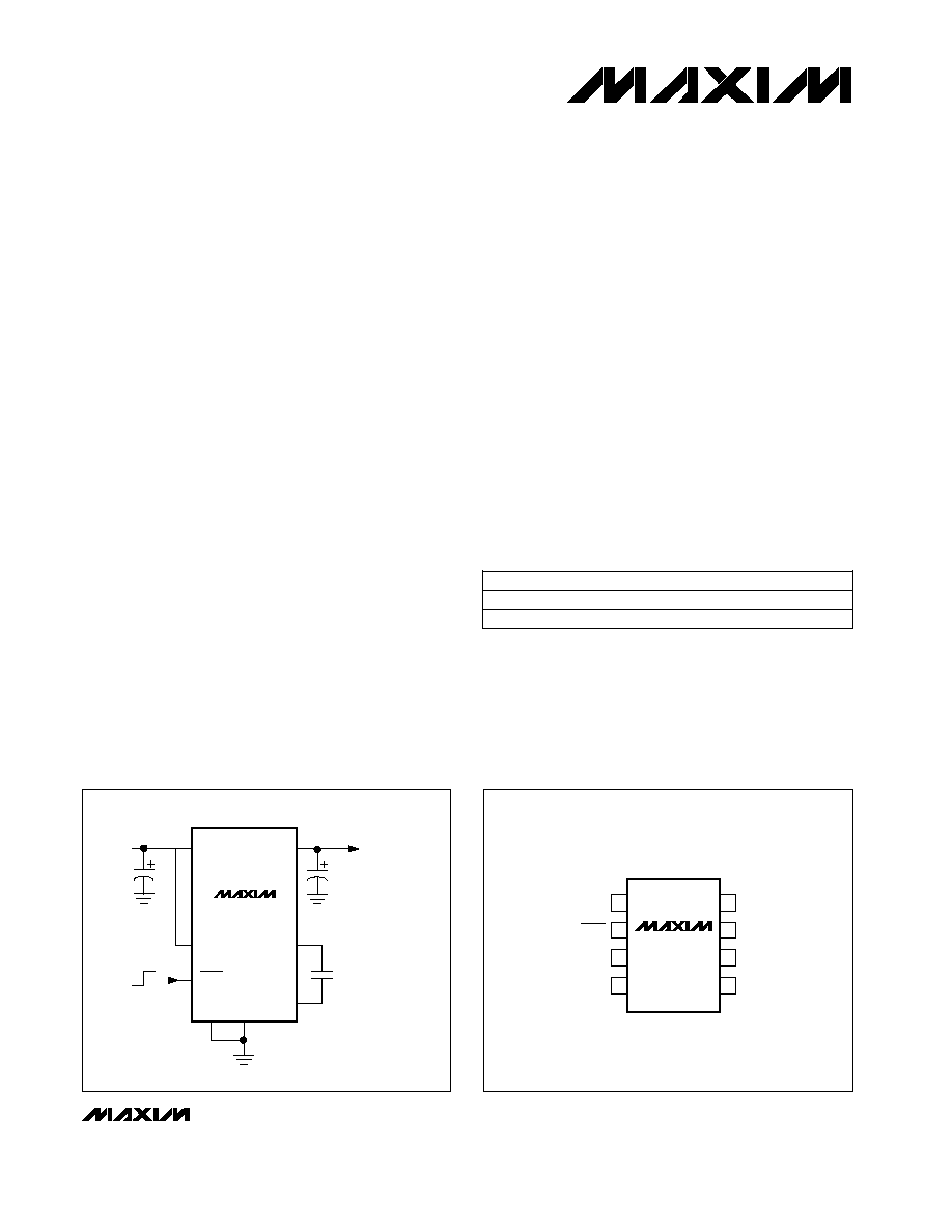
C1-
PGND
GND
1
2
8
7
OUT
C1+
SHDN
IN
FSET
µ
MAX
TOP VIEW
3
4
6
5
MAX679
__________________Pin Configuration
MAX679
OUT
C1+
C1-
OFF/ON
IN
FSET
SHDN
INPUT
2V to 3.6V
OUTPUT
3.3V, 20mA
C
IN
C
OUT
C1
GND
PGND
__________Typical Operating Circuit
19-1217; Rev 0; 4/97
PART
MAX679C/D
0°C to +70°C
TEMP. RANGE
PIN-PACKAGE
Dice*
______________Ordering Information
*
Dice are tested at T
A
= +25°C only.
For free samples & the latest literature: http://www.maxim-ic.com, or phone 1-800-998-8800
MAX679EUA
-40°C to +85°C
8 µMAX
MAX679
Regulated 3.3V Charge Pump
2
_______________________________________________________________________________________
ABSOLUTE MAXIMUM RATINGS
ELECTRICAL CHARACTERISTICS
(V
IN
= V
S HDN
= V
FSET
= 2V, C
IN
= 4.7µF, C1 = 0.33µF, C
OUT
= 10µF,
T
A
= -40°C to +85°C
, unless otherwise noted. Typical values
are at T
A
= +25°C.) (Note 1)
Stresses beyond those listed under "Absolute Maximum Ratings" may cause permanent damage to the device. These are stress ratings only, and functional
operation of the device at these or any other conditions beyond those indicated in the operational sections of the specifications is not implied. Exposure to
absolute maximum rating conditions for extended periods may affect device reliability.
Note 1:
Specifications to -40°C are guaranteed by design, not production tested.
IN, OUT, SHDN, FSET to GND....................................-0.3V to 6V
PGND to GND.....................................................................±0.3V
C1- to GND ..................................................-0.3V to (V
IN
+ 0.3V)
C1+ to GND..............................................-0.3V to (V
OUT
+ 0.3V)
OUT Short to GND ..............................................................10sec
Continuous Power Dissipation (T
A
= +70°C)
µMAX (derate 4.1mW/°C above +70°C) .......................330mW
Operating Temperature Range ...........................-40°C to +85°C
Storage Temperature Range .............................-65°C to +160°C
Lead Temperature (soldering, 10sec) .............................+300°C
FSET = GND
FSET
,
SHDN = GND or V
IN
V
IN
= 2V, I
OUT
= 10mA
V
IN
= 3.6V
V
IN
= 1.8V
V
IN
= 1.8V, V
OUT
> 3.17V
V
IN
= 2.5V, FSET = IN or GND
V
OUT
= 3.6V, SHDN = GND
OUT = GND, V
IN
= 3.3V
V
IN
= 3.3V
FSET = IN
CONDITIONS
%
80
Efficiency
mA
100
200
Output Short-Circuit Current
kHz
700
1000
1300
V
0.8
1.6
V
1.8
3.6
Input Voltage
Input Undervoltage Lockout Voltage
260
330
450
Switching Frequency
µA
0.1
1
FSET, SHDN Input Leakage Current
V
0.7 x
0.5 x
V
IN
V
IN
FSET, SHDN Input Voltage High
V
0.5 x
0.3 x
V
IN
V
IN
FSET, SHDN Input Voltage Low
mA
20
Output Current
µA
50
80
No-Load Supply Current
µA
15
25
Leakage Current into OUT in Shutdown
µA
1
5
Supply Current in Shutdown
UNITS
MIN
TYP
MAX
PARAMETER
2V < V
IN
< 3.3V,
0mA < I
OUT
< 20mA
3.15
3.45
Output Voltage
T
A
= 0°C to +85°C
T
A
= -40°C to +85°C
V
3.17
3.3
3.43
MAX679
Regulated 3.3V Charge Pump
_______________________________________________________________________________________
3
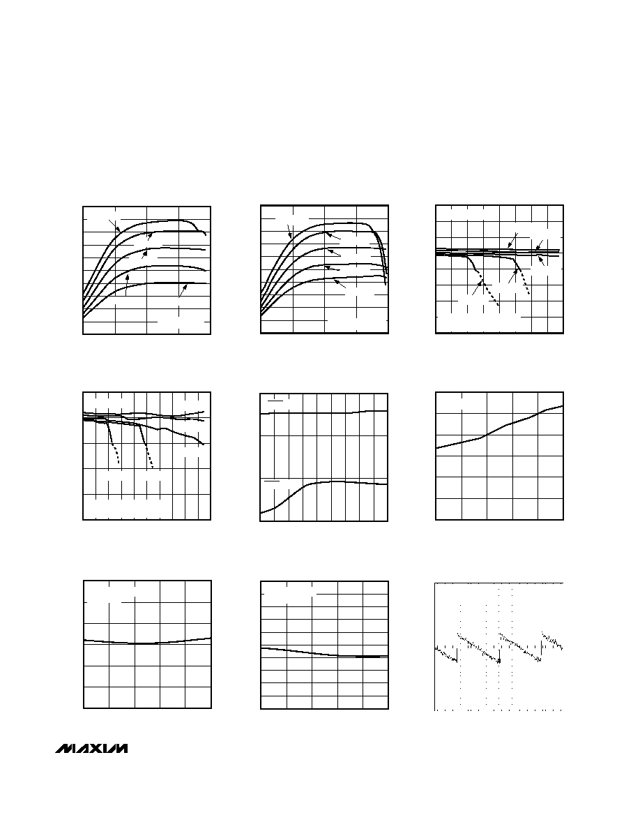
0
EFFICIENCY
vs. OUTPUT CURRENT
20
10
MAX679 TOC01a
OUTPUT CURRENT (mA)
EFFICIENCY (%)
10
50
70
60
40
30
0.01
1
100
90
80
100
0.1
FSET = IN (1MHz)
V
IN
= 3.0V
V
IN
= 3.5V
V
IN
= 2.4V
V
IN
= 2.0V
V
IN
= 1.8V
0
0.01
EFFICIENCY
vs. OUTPUT CURRENT
20
10
30
MAX679 TOC01b
OUTPUT CURRENT (mA)
EFFICIENCY (%)
10
60
50
80
70
40
0.1
100
90
100
1
V
IN
= 3.5V
V
IN
= 3.0V
V
IN
= 2.4V
V
IN
= 2.0V
V
IN
= 1.8V
FSET = GND (330kHz)
2.8
0
OUTPUT VOLTAGE
vs. OUTPUT CURRENT
3.0
2.9
MAX679 TOC02a
OUTPUT CURRENT (mA)
OUTPUT VOLTAGE (V)
3.3
3.4
3.1
3.2
20
30
10
60
70
80
3.5
3.6
40
50
FSET = GND (330kHz)
DASHED LINES INDICATE
OUTPUT OUT OF REGULATION
V
IN
= 3.5V
V
IN
= 3.0V
V
IN
= 2.4V
V
IN
= 2.0V
V
IN
= 1.8V
2.9
0
OUTPUT VOLTAGE
vs. OUTPUT CURRENT
3.0
MAX679 TOC02b
OUTPUT CURRENT (mA)
OUTPUT VOLTAGE (V)
80 90
3.2
3.1
20 30
10
60 70
100
3.3
3.4
40 50
FSET = IN (1MHz)
DASHED LINES INDICATE
OUTPUT OUT OF REGULATION
V
IN
= 3.5V
V
IN
= 3.0V
V
IN
= 2.4V
V
IN
= 2.0V
V
IN
= 1.8V
0.1
1.8
SUPPLY CURRENT
vs. SUPPLY VOLTAGE
MAX679 TOC05
SUPPLY VOLTAGE (V)
SUPPLY CURRENT (
µ
A)
3.2 3.4
10
1
2.2
2.0
3.0
3.6
100
2.6
2.8
2.4
SHDN = IN
SHDN = GND
0
-40
SHUTDOWN SUPPLY CURRENT
vs. TEMPERATURE
100
MAX679 TOC06
TEMPERATURE (°C)
SHUTDOWN SUPPLY CURRENT (nA)
60
300
400
200
-15
35
85
500
600
10
V
IN
= 2.4V
__________________________________________Typical Operating Characteristics
(Typical Operating Circuit with: V
IN
= V
S HDN
= 2V, C
IN
= 4.7µF, C1 = 0.33µF, C
OUT
= 10µF, tested in-circuit, T
A
= +25°C, unless
otherwise noted.)
300
-40
PUMP FREQUENCY
vs. TEMPERATURE
310
MAX679 TOC08a
TEMPERATURE (°C)
PUMP FREQUENCY (kHz)
60
330
340
320
-15
35
85
350
360
10
FSET = GND (330kHz)
V
IN
= 2.5V
900
-40
PUMP FREQUENCY
vs. TEMPERATURE
940
920
960
MAX679 TOC08b
TEMPERATURE (°C)
PUMP FREQUENCY (kHz)
60
1020
1000
1060
1040
980
-15
35
85
1080
1100
10
FSET = IN (1MHz)
V
IN
= 2.5V
OUTPUT RIPPLE (2mA LOAD)
MAX679 TOC09
V
OUT
50mV/div
AC COUPLED
100
µ
s/div
FSET = GND (330kHz)
MAX679
Regulated 3.3V Charge Pump
4
_______________________________________________________________________________________
____________________________Typical Operating Characteristics (continued)
(Typical Operating Circuit with: V
IN
= V
S HDN
= 2V, C
IN
= 4.7µF, C1 = 0.33µF, C
OUT
= 10µF, tested in-circuit, T
A
= +25°C, unless
otherwise noted.)
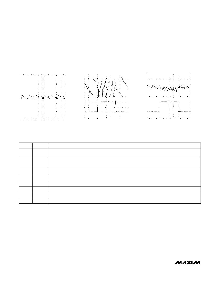
______________________________________________________________Pin Description
NAME
FUNCTION
1
FSET
Set Charge-Pump Frequency Input. FSET = GND selects 330kHz and FSET = IN selects 1MHz. Do not leave
FSET unconnected.
2
SHDN
Shutdown Input. The device shuts down, the output disconnects from the input, and the supply current
decreases to 1µA when SHDN is a logic low. Connect SHDN to IN for normal operation.
PIN
3
IN
Supply Input. Connect to an input supply in the 1.8V to 3.6V range. Bypass IN to GND with a (C
OUT
/ 2)µF
capacitor.
4
GND
Ground. Analog ground for internal reference and control circuitry.
8
OUT
3.3V Power Output. Bypass OUT to GND with an output filter capacitor (see the
Design Procedure section).
7
C1+
Positive Terminal of the Charge-Pump Capacitor
6
C1-
Negative Terminal of the Charge-Pump Capacitor
5
PGND
Power Ground. Charge-pump current flows through this pin.
LOAD-TRANSIENT RESPONSE
(1mA TO 10mA LOAD, V
IN
= 3V)
MAX679 TOC11
V
OUT
10mV/div
AC COUPLED
I
OUT
5mA/div
100
µ
s/div
V
IN
= 3V
FSET = IN (1MHz)
LOAD-TRANSIENT RESPONSE
(1mA TO 10mA LOAD, V
IN
= 2V)
MAX679 TOC12
V
OUT
10mV/div
AC COUPLED
I
OUT
5mA/div
50
µ
s/div
V
IN
= 2V
FSET = IN (1MHz)
_______________Detailed Description
The MAX679 regulated charge pump has a 50% duty-
cycle clock. In phase one (charge phase), the charge-
transfer capacitor (C1) charges to the input voltage,
and output current is delivered by the output filter
capacitor (C
OUT
). In phase two (transfer phase), C1 is
placed in series with the input and connects to the out-
put, transferring its charge to C
OUT
. If the clock were to
run continuously, this process would eventually gener-
ate an output voltage equal to two times the input volt-
age (hence the name "doubler").
The charge pump regulates by gating the oscillator on
and off as needed to maintain output regulation. This
method has low quiescent current, but to achieve
acceptable output ripple, C1 must be significantly
lower in value than C
OUT
.
Start-Up Sequence
The MAX679 soft-start circuitry prevents excessive cur-
rent from being drawn from the battery at start-up or
when the output is shorted. This is done by limiting the
charge pump to 1/10 the normal current until either the
output is in regulation or the first 4096 charge-pump
OUTPUT RIPPLE (2mA LOAD)
MAX679 TOC10
V
OUT
50mV/div
AC COUPLED
100
µ
s/div
FSET = IN (1MHz)
MAX679
Regulated 3.3V Charge Pump
_______________________________________________________________________________________
5
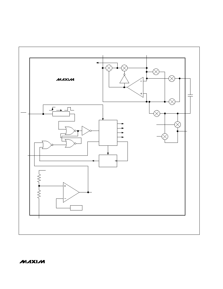
P6
IN
OUT
P5
P4
SW
P3
T
C
P2
PGND
C1-
C1
C1+
10% OF N1
SC
C
N1
T
P1
PULSER
SW
C
T
SC
CLOCK
RESET
2
12
COUNTER
OSCILLATOR +
CONTROL LOGIC
CHIP SUPPLY
OUT
FSET
SHDN
1.25V REF
GND
EAOUT (1 = OUTPUT OVER REGULATION POINT)
MAX679
SW
T
C
SC
SWITCH CONNECTS OUT TO IN DURING START-UP
TRANSFER PHASE OF PUMP
CHARGE PHASE OF PUMP (FULL STRENGTH)
CHARGE PHASE OF PUMP (REDUCED STRENGTH)
=
=
=
=
Figure 1. Block Diagram