 | ÐлекÑÑоннÑй компоненÑ: MAX555CCB | СкаÑаÑÑ:  PDF PDF  ZIP ZIP |
MAX555 DS
General Description
The MAX555 is an advanced, monolithic, 12-bit digital-
to-analog converter (DAC) with complementary 50
outputs. Fabricated using an oxide-isolated bipolar
process, the MAX555 is designed for signal-reconstruc-
tion applications at an output update rate of 300Msps.
It incorporates an analog multiplying function with
10MHz useable input bandwidth. The voltage-output
DAC uses precision laser trimming to achieve 12-bit
accuracy with ±1/2LSB integral and differential linearity
(±0.012% FS). Absolute gain error is a low 1% of full
scale. Full-scale transitions occur in less than 0.5ns.
Internal registers and a unique decoder reduce glitch-
ing and allow the MAX555 to achieve precise RF perfor-
mance with over 73dBc of spurious-free dynamic range
at 50Msps with f
OUT
= 3.1MHz, or 62dBc at 300Msps
with f
OUT
= 18.6MHz.
The MAX555 operates from a single -5.2V supply and
dissipates 980mW (nominal). It comes in a 64-pin TQFP
package with exposed paddle for enhanced thermal
dissipation.
________________________Applications
Direct Digital Synthesis
Arbitrary Waveform Generation
HDTV/High-Resolution Graphics
Instrumentation
Communications Local Oscillators
Automated Tester Applications
____________________________Features
o 12-Bit Resolution
o ±1/2LSB Integral and Differential Nonlinearity
o Capable of 300Msps (min) Update Rate
o Complementary 50 Outputs
o Multiplying Reference Input
o Low Glitch Energy (5.6pVs)
o Single -5.2V Power Supply
o On-Chip Data Registers
o ECL-Compatible Inputs with Differential Clock
Ordering Information
MAX555
300Msps, 12-Bit DAC with
Complementary Voltage Outputs
________________________________________________________________ Maxim Integrated Products
1
-20mA
LGND
VOUT
VOUT
CLK
CLK
ROFFSET
REF
50
800
800
50
AV
EE
BYPASS
DECODED
BIT
LINES
12-BIT
ECL
LINES
LEVEL-SENSITIVE TRANSPARENT LATCH
MAX555
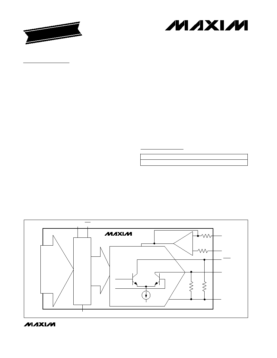
___________________________________________________Simplified Block Diagram
19-0297; Rev 3; 6/02
PART
MAX555CCB
0°C to +70°C
TEMP RANGE
PIN-PACKAGE
64 TQFP-EP*
Pin Configuration appears at end of data sheet.
EVALUATION KIT MANUAL
AVAILABLE
For pricing, delivery, and ordering information, please contact Maxim/Dallas Direct! at
1-888-629-4642, or visit Maxim's website at www.maxim-ic.com.
*EP = Exposed pad.
MAX555
300Msps, 12-Bit DAC with
Complementary Voltage Outputs
2
_______________________________________________________________________________________
ABSOLUTE MAXIMUM RATINGS
ELECTRICAL CHARACTERISTICS
(AV
EE
= DV
EE
= -5.2V, V
REF
= 1.000V, T
MIN
to T
MAX
= 0°C to +70°C, unless otherwise noted.) (Note 2.)
Stresses beyond those listed under "Absolute Maximum Ratings" may cause permanent damage to the device. These are stress ratings only, and functional
operation of the device at these or any other conditions beyond those indicated in the operational sections of the specifications is not implied. Exposure to
absolute maximum rating conditions for extended periods may affect device reliability.
Note 1: Typical thermal resistance, junction-to-case R
JC
= 25°C/W. See Package Information.
Analog Supply Voltage (AV
EE
) .................................-7V to +0.3V
Digital Supply Voltage (DV
EE
) ..................................-7V to +0.3V
Digital Input Voltage (D0D11) ...................................-5.5V to 0V
Reference Input Voltage (V
IN
) .................................0V to +1.25V
Reference Input Current....................................0mA to +1.56mA
Output Compliance Voltage (V
OC
)......................-1.25V to +1.0V
Output Common-Mode Voltage (V
CM
) ................-0.25V to +1.0V
Continuous Power Dissipation (T
A
= +70°C)
(without additional heatsink) ..............................................1.3W
Operating Temperature Range...............................0°C to +70°C
Junction Temperature Range (Note 1) .................0°C to +150°C
Storage Temperature Range .............................-65°C to +150°C
Lead Temperature (soldering, 10s) .................................+300°C
V
REF
= 1.000V, current out, into
virtual ground, end-point linearity
Major carry, T
A
= +25°C
10% to 90%, T
A
= +25°C
90% to 10%, T
A
= +25°C
V
REF
= 1.000V, voltage out, VOUT/VIN (Note 3)
±0.024% FS, 1LSB change
D0D11 = logic 1, V
REF
= 1.000V,
measured at VOUT
±0.1% FS
CONDITIONS
ns
15
Settling Time
4
% FS
-0.05
±0.01
0.05
DLE2
Differential Linearity Error
-0.012
±0.003
0.012
DLE1
pVs
5.6
Glitch Energy
ps
570
t
RISE
Rise Time
ps
410
t
FALL
Fall Time
% FS
-1.0
±0.2
+1.0
GE
Absolute Gain Error
Guaranteed
12-Bit Monotonicity
µA
40
100
I
OS
Output Offset Current
UNITS
MIN
TYP
MAX
SYMBOL
PARAMETER
VOUT
VOUT
V
REF
= 1.000V, current out, into
virtual ground, end-point linearity
VOUT
% FS
-0.05
±0.01
0.05
ILE2
Integral Linearity Error
VOUT
-0.012
±0.006
0.012
ILE1
D0D11 = logic 0, V
REF
= 0V,
measured at VOUT
µA
3
50
I
LEAK
Output Leakage Current
f
OUT
= 5MHz, f
CLK
= 50MHz
72
f
OUT
= 20MHz, f
CLK
= 100MHz
f
OUT
= 10MHz, f
CLK
= 50MHz
63
68
f
OUT
= 30MHz, f
CLK
= 200MHz
f
OUT
= 30MHz, f
CLK
= 100MHz
57
58
f
OUT
= 40MHz, f
CLK
= 200MHz
54
dBc
f
OUT
= 40MHz, f
CLK
= 250MHz
53
f
OUT
= 40MHz, f
CLK
= 300MHz
f
OUT
= 50MHz, f
CLK
= 250MHz
54
51
f
OUT
= 50MHz, f
CLK
= 300MHz
SFDR
Spurious-Free Dynamic Range
51
nV
Hz
Bits 011 high, T
A
= +25°C
10.6
Output Noise
DC ACCURACY
TIME-DOMAIN PERFORMANCE (Note 4)
DYNAMIC PERFORMANCE (Notes 4, 5)
MAX555
300Msps, 12-Bit DAC with
Complementary Voltage Outputs
_______________________________________________________________________________________
3
ELECTRICAL CHARACTERISTICS (continued)
(AV
EE
= DV
EE
= -5.2V, V
REF
= 1.000V, T
MIN
to T
MAX
= 0°C to +70°C, unless otherwise noted.) (Note 2.)
AV
EE
= DV
EE
= -5.2V
AV
EE
= DV
EE
= -5.2V
V
IL
= -1.95V
VOUT, VOUT
VOUT, VOUT
V
IH
= -0.75V
V
REF
= 1.000V, R
L
= 0
T
A
= +25°C
T
A
= +25°C
Bypass = 1, transparent mode (Notes 4, 7)
Bypass = 1, transparent mode (Notes 4, 7)
-3dB
V
REF
= 1.000V
Bypass = 0, clocked mode (Notes 4, 7)
Bypass = 0, clocked mode (Notes 4, 7)
Bypass = 0, clocked mode (Notes 4, 7)
Bypass = 1, transparent mode (Notes 4, 7)
CONDITIONS
mA
110
150
190
DI
EE
Digital Power-Supply Current
mA
30
46
60
AI
EE
Analog Power-Supply Current
pF
15
C
OUT
Output Capacitance
49.5
50.0
50.5
R
OUT
Output Resistance
mA
19.0
20.0
21.0
I
OUT
Full-Scale Output Current
µV
-250
0
+250
V
OS
Input Offset Voltage
kV/V
3
20
AV
OL
Open-Loop Gain
MHz
10
BW
Multiplying Input Bandwidth
775
800
825
R
IN
Amplifier Input Resistance
ps
900
t
DD
MSBs Decode Delay
µA
1
2
I
IL
Input Current, Logic Low
µA
10
200
I
IH
Input Current, Logic High
ns
2.9
t
PD1
MSBs Data-to-VOUT
Propagation Delay
ns
2
t
PD2
LSBs Data-to-VOUT
Propagation Delay
ns
2.8
t
PD3
Clock-to-VOUT
Propagation Delay
ns
0.8
t
HOLD
Data-to-Clock Hold Time
V
-1.1
-0.75
0
V
IH
Logic "1" Voltage
V
-2.0
-1.95
-1.48
V
IL
Logic "0" Voltage
ns
1
t
SU
Data-to-Clock Setup Time
UNITS
MIN
TYP
MAX
SYMBOL
PARAMETER
W
0.98
1.3
P
DISS
Power Dissipation
°C/W
25
T
JA
Package Thermal Resistance,
Junction to Ambient
Note 2: All devices are 100% production tested at +25°C and are guaranteed by design for T
A
= T
MIN
to T
MAX
as specified.
Note 3: The gain-error method of calculation is shown below:
Definition:
[V
MEASURE(FS)
- V
IDEAL(FS)
] x 100
GE(%) =
V
IDEAL(FS)
where FS indicates full-scale measurements.
GE Method:
GE(%) = [(4096 / 4095) V
MEASURE
- 16(V
REF
/ R
IN
) (R
OUT
)] x 100
----
16(V
REF
/ R
IN
) (R
OUT
)
= [(4096 / 4095) V
MEASURE
- 1] x 100
1
where: V
REF
= 1.000V, R
IN
= 800
, R
OUT
= 50
, V
MEASURE
= VOUT (FS).
Note 4: Dynamic and timing specifications are obtained from device characterization and simulation testing and are not production tested.
Note 5: Spurious-free dynamic range is measured from the fundamental frequency to any harmonic or nonharmonic spurs within the
bandwidth f
CLK
/2, unless otherwise specified.
Note 6: Guaranteed by design.
Note 7: Timing definitions are detailed in Figure 2.
Minimum data rate = DC (Note 6)
MHz
300
f
D
Data Update Rate
DIGITAL INPUTS
CONTROL AMPLIFIER
OUTPUT PERFORMANCE
POWER SUPPLIES
DIGITAL TIMING
MAX555
300Msps, 12-Bit DAC with
Complementary Voltage Outputs
4
_______________________________________________________________________________________
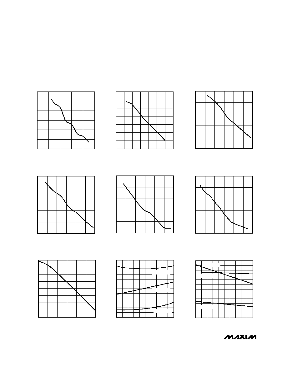
__________________________________________Typical Operating Characteristics
(AV
EE
= DV
EE
= -5.2V, V
REF
= 0.75V, T
A
= +25°C, unless otherwise noted.)
62
66
64
70
68
72
74
0
8
4
12
16
20
SPURIOUS-FREE DYNAMIC RANGE
vs. f
OUT
(f
CLK
= 50MHz)
MAX555-01
f
OUT
(MHz)
SFDR (dBc)
60
64
62
68
66
72
70
74
0
8
12
4
16
20
24
28
SPURIOUS-FREE DYNAMIC RANGE
vs. f
OUT
(f
CLK
= 100MHz)
MAX555-02
f
OUT
(MHz)
SFDR (dBc)
50
54
62
58
66
70
0
12
6
18
24
30
36
SPURIOUS-FREE DYNAMIC RANGE
vs. f
OUT
(f
CLK
= 150MHz)
MAX555-03
f
OUT
(MHz)
SFDR (dBc)
74
SPURIOUS-FREE DYNAMIC RANGE
vs. f
CLK
(f
OUT
~ 1/16 f
CLK
)
58
70
MAX555-07
CLOCK FREQUENCY (MHz)
SFDR (dB)
350
300
250
200
150
100
50
66
62
60
72
68
64
-48
0.5
0.6
0.7
0.8
0.9
1.0
3RD HARMONIC DISTORTION
vs. V
REF
VOLTAGE (f
OUT
~ 1/5 f
CLK
)
-52
MAX555-08
V
REF
(V)
3RD HARMONIC (dBc)
-56
-50
-54
-58
-60
-62
-64
-66
-68
-70
-72
f
CLK
= 100MHz
f
CLK
= 200MHz
f
CLK
= 300MHz
-48
0.5
0.6
0.7
0.8
0.9
1.0
2ND HARMONIC DISTORTION
vs. V
REF
VOLTAGE (f
OUT
~ 1/5 f
CLK
)
-52
MAX555-09
V
REF
(V)
3RD HARMONIC (dBc)
-56
-50
-54
-58
-60
-62
-64
-66
-68
-70
-72
f
CLK
= 100MHz
f
CLK
= 200MHz
f
CLK
= 300MHz
52
56
64
60
68
72
0
12
6
18
24
30
36
SPURIOUS-FREE DYNAMIC RANGE
vs. f
OUT
(f
CLK
= 200MHz)
MAX555-04
f
OUT
(MHz)
SFDR (dBc)
52
56
64
60
68
72
0
14
7
21
28
35
42
SPURIOUS-FREE DYNAMIC RANGE
vs. f
OUT
(f
CLK
= 250MHz)
MAX555-05
f
OUT
(MHz)
SFDR (dBc)
50
54
62
58
66
70
0
20
10
30
40
50
60
SPURIOUS-FREE DYNAMIC RANGE
vs. f
OUT
(f
CLK
= 300MHz)
MAX555-06
f
OUT
(MHz)
SFDR (dBc)
MAX555
300Msps, 12-Bit DAC with
Complementary Voltage Outputs
_______________________________________________________________________________________
5
_______________Detailed Description
Figure 1's functional diagram shows the MAX555's three
major divisions: a digital section, a control-amplifier sec-
tion, and a resistor-divider network. The digital section
consists of a master/slave register, decoding logic, and
current switches. The control-amplifier section includes a
control amplifier and an array of 23 current sources divid-
ed into three groups. The resistor divider scales the cur-
rents from these groups to achieve the correct binary
weighting at the output. The output of the resistor-divider
network is laser trimmed to 50
, a key feature for driving
into controlled impedance transmission lines.
The first group of current sources comprises the six
MSBs, D11D6 (resulting in 15 identical, plus two binary
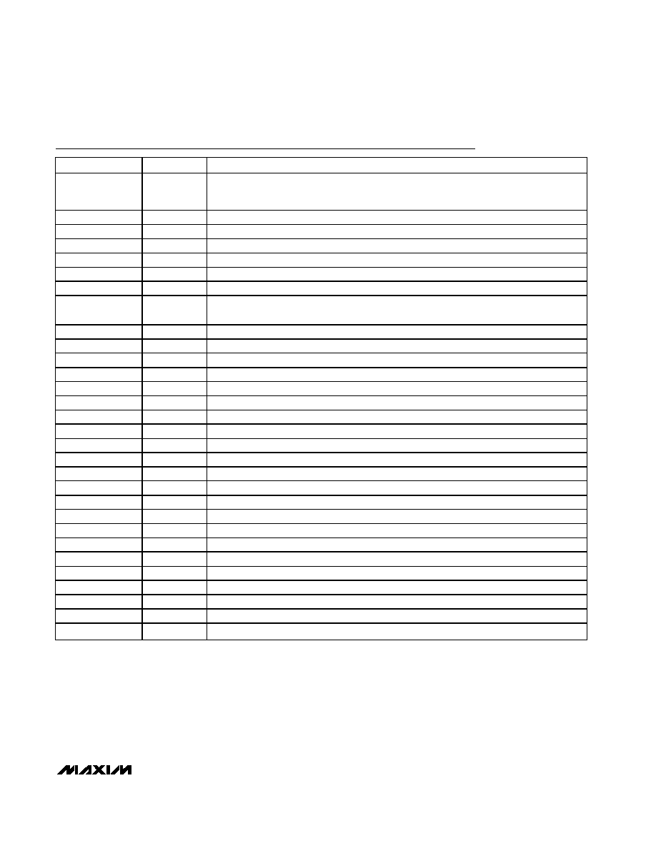
Pin Description
PIN
NAME
FUNCTION
1, 14, 1619, 27,
28, 29, 3138, 48,
49, 64
AGND
Analog Ground. Note: Exposed pad on the back of the package must be connected to
AGND.
2, 6, 54, 60
DGND
Digital Ground
3
D8
Data Bit 8 (ECL Input)
4
D9
Data Bit 9 (ECL Input)
5
D10
Data Bit 10 (ECL Input)
7, 53
DV
EE
-5.2V Digital Power Supply
8
D11
Data Bit 11 (ECL Input)--MSB
9, 10, 11, 13, 39,
46, 58
N.C.
No Connection
12
LBIAS
Ladder-Bias Alternate Compensation Output. Connect bypass capacitor to AV
EE
.
15
ALTCOMPC
Control-Amplifier PTAT Reference Compensation Input. Connect bypass capacitor to AV
EE
.
20
ROFFSET
Offset Compensation Input
21, 22
REF
Analog Reference Voltage Inputs (Kelvin Connection)
23
REF/2
Analog Reference Voltage Center-Tap Input
24, 25
AV
EE
-5.2V Analog Power Supply
26
LOOPCRNT
Test Node. Must connect to AGND.
30
ALTCOMPIB
PTAT-IB Reference Compensation Output. Connects bypass capacitor to AV
EE
.
40, 41
VOUT
Complementary DAC Output
42, 43
LGND
Ladder Ground
44, 45
VOUT
DAC Output
47
D0
Data Bit 0 (ECL Input)--LSB
50
D1
Data Bit 1 (ECL Input)
51
D2
Data Bit 2 (ECL Input)
52
D3
Data Bit 3 (ECL Input)
55
CLK
Complementary Clock Input (ECL Input)
56
CLK
Clock Input (ECL Input)
57
BYPASS
Disables Latching of Data when High (ECL Input)
59
D4
Data Bit 4 (ECL Input)
61
D5
Data Bit 5 (ECL Input)
62
D6
Data Bit 6 (ECL Input)
63
D7
Data Bit 7 (ECL Input)