 | –≠–ª–µ–∫—Ç—Ä–æ–Ω–Ω—ã–π –∫–æ–º–ø–æ–Ω–µ–Ω—Ç: MAX5418 | –°–∫–∞—á–∞—Ç—å:  PDF PDF  ZIP ZIP |

General Description
The MAX5417/MAX5418/MAX5419 nonvolatile, linear-
taper, digital potentiometers perform the function of a
mechanical potentiometer, but replace the mechanics
with a simple 2-wire digital interface, allowing communi-
cation with multiple devices. Each device performs the
same function as a discrete potentiometer or variable
resistor and has 256 tap points.
The devices feature an internal, nonvolatile EEPROM
used to store the wiper position for initialization during
power-up. The fast-mode I
2
CTM-compatible serial inter-
face allows communication at data rates up to 400kbps,
minimizing board space and reducing interconnection
complexity in many applications. Each device is available
with one of four factory-preset addresses (see the
Selector Guide) and features an address input for a total
of eight unique address combinations.
The MAX5417/MAX5418/MAX5419 provide three nomi-
nal resistance values: 50k
(MAX5417), 100k
(MAX5418), or 200k
(MAX5419). The nominal resistor
temperature coefficient is 35ppm/∞C end-to-end, and
only 5ppm/∞C ratiometric. This makes the devices ideal
for applications requiring a low-temperature-coefficient
variable resistor, such as low-drift, programmable gain-
amplifier circuit configurations.
The MAX5417/MAX5418/MAX5419 are available in a
3mm x 3mm 8-pin TDFN package, and are specified
over the extended -40∞C to +85∞C temperature range.
Applications
Mechanical Potentiometer Replacement
Low-Drift Programmable-Gain Amplifiers
Volume Control
Liquid-Crystal Display (LCD) Contrast Control
Features
Power-On Recall of Wiper Position from
Nonvolatile Memory
Tiny 3mm x 3mm 8-Pin TDFN Package
35ppm/∞C End-to-End Resistance Temperature
Coefficient
5ppm/∞C Ratiometric Temperature Coefficient
50k/100k/200k Resistor Values
Fast I
2
C-Compatible Serial Interface
500nA (typ) Static Supply Current
Single-Supply Operation: +2.7V to +5.25V
256 Tap Positions
±0.5 LSB DNL in Voltage-Divider Mode
±0.5 LSB INL in Voltage-Divider Mode
MAX5417/MAX5418/MAX5419
256-Tap, Nonvolatile, I
2
C-Interface,
Digital Potentiometers
________________________________________________________________ Maxim Integrated Products
1
V
DD
GND
SDA
SCL
8-BIT
SHIFT
REGISTER
8-BIT
LATCH
8-BIT
NV
MEMORY
I
2
C
INTERFACE
A
0
8
8
256
W
L
256-
POSITION
DECODER
H
POR
MAX5417
MAX5418
MAX5419
Ordering Information/Selector Guide
Functional Diagram
19-3185; Rev 2; 8/04
For pricing, delivery, and ordering information, please contact Maxim/Dallas Direct! at
1-888-629-4642, or visit Maxim's website at www.maxim-ic.com.
Pin Configuration appears at end of data sheet.
I
2
C is a trademark of Phillips Corp.
Purchase of I
2
C components from Maxim Integrated Products,
Inc. or one of its sublicensed Associated Companies, conveys
a license under the Philips I
2
C Patent Rights to use these com-
ponents in an I
2
C system, provided that the system conforms
to the I
2
C Standard Specification as defined by Philips.
*Future product--contact factory for availability.
**Exposed pad.
PART
TEMP RANGE
I
2
C ADDRESS
R (k
)
PIN-PACKAGE
TOP MARK
MAX5417LETA
-40∞C to +85∞C
010100A
0
50
8 TDFN-EP**
AIB
MAX5417META*
-40∞C to +85∞C
010101A
0
50
8 TDFN-EP**
ALS
MAX5417NETA*
-40∞C to +85∞C
010110A
0
50
8 TDFN-EP**
ALT
MAX5417PETA*
-40∞C to +85∞C
010111A
0
50
8 TDFN-EP**
ALU
MAX5418LETA
-40∞C to +85∞C
010100A
0
100
8 TDFN-EP**
AIC
MAX5418META*
-40∞C to +85∞C
010101A
0
100
8 TDFN-EP**
ALV
MAX5418NETA*
-40∞C to +85∞C
010110A
0
100
8 TDFN-EP**
ALW
MAX5418PETA*
-40∞C to +85∞C
010111A
0
100
8 TDFN-EP**
ALX
MAX5419LETA
-40∞C to +85∞C
010100A
0
200
8 TDFN-EP**
AID
MAX5419META*
-40∞C to +85∞C
010101A
0
200
8 TDFN-EP**
ALY
MAX5419NETA*
-40∞C to +85∞C
010110A
0
200
8 TDFN-EP**
ALZ
MAX5419PETA*
-40∞C to +85∞C
010111A
0
200
8 TDFN-EP**
AMA
MAX5417/MAX5418/MAX5419
256-Tap, Nonvolatile, I
2
C-Interface,
Digital Potentiometers
2
_______________________________________________________________________________________
ABSOLUTE MAXIMUM RATINGS
ELECTRICAL CHARACTERISTICS
(V
DD
= +2.7V to +5.25V, H = V
DD
, L = GND, T
A
= -40∞C to +85∞C, unless otherwise noted. Typical values are at V
DD
= +5V, T
A
= +25∞C.)
Stresses beyond those listed under "Absolute Maximum Ratings" may cause permanent damage to the device. These are stress ratings only, and functional
operation of the device at these or any other conditions beyond those indicated in the operational sections of the specifications is not implied. Exposure to
absolute maximum rating conditions for extended periods may affect device reliability.
V
DD
to GND ...........................................................-0.3V to +6.0V
All Other Pins to GND.................................-0.3V to (V
DD
+ 0.3V)
Maximum Continuous Current into H, L, and W
MAX5417......................................................................
±1.3mA
MAX5418......................................................................
±0.6mA
MAX5419......................................................................
±0.3mA
Continuous Power Dissipation (T
A
= +70∞C)
8-Pin TDFN (derate 24.4mW/∞C above +70∞C) .........1951mW
Operating Temperature Range ...........................-40∞C to +85∞C
Junction Temperature ......................................................+150∞C
Storage Temperature Range .............................-60∞C to +150∞C
Lead Temperature (soldering, 10s) .................................+300∞C
PARAMETER
SYMBOL
CONDITIONS
MIN
TYP
MAX
UNITS
DC PERFORMANCE (VOLTAGE-DIVIDER MODE)
Resolution
256
Taps
Integral Nonlinearity
INL
(Note 1)
±0.5
LSB
Differential Nonlinearity
DNL
(Note 1)
±0.5
LSB
End-to-End Temperature
Coefficient
TC
R
35
ppm/∞C
Ratiometric Temperature
Coefficient
5
ppm/∞C
MAX5417_, 50
-0.6
MAX5418_, 100k
-0.3
Full-Scale Error
MAX5419_, 200k
-0.15
LSB
MAX5417_, 50k
0.6
MAX5418_, 100k
0.3
Zero-Scale Error
MAX5419_, 200k
0.15
LSB
DC PERFORMANCE (VARIABLE-RESISTOR MODE)
V
DD
= 3V
±3
Integral Nonlinearity
(Note 2)
INL
V
DD
= 5V
±1.5
LSB
V
DD
= 3V, MAX5417_, 50k
,
guaranteed monotonic
-1
+2
V
DD
= 3V, MAX5418_, 100k
±1
MAX5419_, 200k
±1
Differential Nonlinearity
(Note 2)
DNL
V
DD
= 5V
±1
LSB
DC PERFORMANCE (RESISTOR CHARACTERISTICS)
Wiper Resistance
R
W
V
DD
= 3V to 5.25V (Note 3)
325
675
Wiper Capacitance
C
W
10
pF
MAX5417_
37.5
50
62.5
MAX5418_
75
100
125
End-to-End Resistance
R
HL
MAX5419_
150
200
250
k
MAX5417/MAX5418/MAX5419
256-Tap, Nonvolatile, I
2
C-Interface,
Digital Potentiometers
_______________________________________________________________________________________
3
ELECTRICAL CHARACTERISTICS (continued)
(V
DD
= +2.7V to +5.25V, H = V
DD
, L = GND, T
A
= -40∞C to +85∞C, unless otherwise noted. Typical values are at V
DD
= +5V, T
A
= +25∞C.)
PARAMETER
SYMBOL
CONDITIONS
MIN
TYP
MAX
UNITS
DIGITAL INPUTS
V
DD
= 3.4V to 5.25V
2.4
Input High Voltage (Note 4)
V
IH
V
DD
< 3.4V
0.7 x V
DD
V
Input Low Voltage
V
IL
V
DD
= 2.7V to 5.25V (Note 4)
0.8
V
Low-Level Output Voltage
V
OL
3mA sink current
0.4
V
Input Leakage Current
I
LEAK
±1
µA
Input Capacitance
5
pF
DYNAMIC CHARACTERISTICS
MAX5417_
100
MAX5418_
50
Wiper -3dB Bandwidth (Note 5)
MAX5419_
25
kHz
NONVOLATILE MEMORY
Data Retention
T
A
= +85∞C
50
Years
T
A
= +25∞C
200,000
Endurance
T
A
= +85∞C
50,000
Stores
POWER SUPPLY
Power-Supply Voltage
V
DD
2.70
5.25
V
Standby Current
I
DD
Digital inputs = V
DD
or GND,
T
A
= +25∞C
0.5
1
µA
Programming Current
During nonvolatile write;
digital inputs = V
DD
or GND (Note 6)
200
400
µA
PARAMETER
SYMBOL
CONDITIONS
MIN
TYP
MAX
UNITS
ANALOG SECTION
MAX5417_
500
MAX5418_
600
Wiper Settling Time (Note 8)
t
IL
MAX5419_
1000
ns
DIGITAL SECTION
SCL Clock Frequency
f
SCL
400
kHz
Setup Time for START Condition
t
SU-STA
0.6
µs
Hold Time for START Condition
t
HD-STA
0.6
µs
CLK High Time
t
HIGH
0.6
µs
CLK Low Time
t
LOW
1.3
µs
TIMING CHARACTERISTICS
(V
DD
= +2.7V to +5.25V, H = V
DD
, L = GND, T
A
= -40∞C to +85∞C, unless otherwise noted. Typical values are at V
DD
= +5V, T
A
=
+25∞C. See Figures 1 and 2.) (Note 7)
MAX5417/MAX5418/MAX5419
256-Tap, Nonvolatile, I
2
C-Interface,
Digital Potentiometers
4
_______________________________________________________________________________________
Note 1:
The DNL and INL are measured with the potentiometer configured as a voltage-divider with H = V
DD
and L = GND. The
wiper terminal is unloaded and measured with a high-input-impedance voltmeter.
Note 2:
The DNL and INL are measured with the potentiometer configured as a variable resistor. H is unconnected and L = GND.
For the 5V condition, the wiper terminal is driven with a source current of 80µA for the 50k
configuration, 40µA for the
100k
configuration, and 20µA for the 200k configuration. For the 3V condition, the wiper terminal is driven with a source
current of 40µA for the 50k
configuration, 20µA for the 100k configuration, and 10µA for the 200k configuration.
Note 3:
The wiper resistance is measured using the source currents given in Note 2. For operation to V
DD
= 2.7V, see Wiper
Resistance vs. Temperature in the Typical Operating Characteristics.
Note 4:
The device draws higher supply current when the digital inputs are driven with voltages between (V
DD
- 0.5V) and (GND +
0.5V). See Supply Current vs. Digital Input Voltage in the Typical Operating Characteristics.
Note 5:
Wiper at midscale with a 10pF load (DC measurement). L = GND; an AC source is applied to H; and the W output is mea-
sured. A 3dB bandwidth occurs when the AC W/H value is 3dB lower than the DC W/H value.
Note 6:
The programming current operates only during power-up and NV writes.
Note 7:
SCL clock period includes rise and fall times t
R
and t
F
. All digital input signals are specified with t
R
= t
F
= 2ns and timed
from a voltage level of (V
IL
+ V
IH
) / 2.
Note 8:
Wiper settling time is the worst-case 0% to 50% rise time measured between consecutive wiper positions. H = V
DD
,
L = GND, and the wiper terminal is unloaded and measured with a 10pF oscilloscope probe (see the Typical Operating
Characteristics for the tap-to-tap switching transient).
Note 9:
An appropriate bus pullup resistance must be selected depending on board capacitance. Refer to the document linked to
this web address: www.semiconductors.philips.com/acrobat/literature/9398/39340011.pdf.
Note 10: The idle time begins from the initiation of the stop pulse.
PARAMETER
SYMBOL
CONDITIONS
MIN
TYP
MAX
UNITS
Data Setup Time
t
SU-DAT
100
ns
Data Hold Time
t
HD-DAT
0
0.9
µs
SDA, SCL Rise Time
t
R
300
ns
SDA, SCL Fall Time
t
F
300
ns
Setup Time for STOP Condition
t
SU-STO
0.6
µs
Bus Free Time Between STOP
and START Condition
t
BUF
Minimum power-up rate = 0.2V/ms
1.3
µs
Pulse Width of Spike Suppressed
t
SP
50
ns
Maximum Capacitive Load for
Each Bus Line
C
B
(Note 9)
400
pF
Write NV Register Busy Time
t
BUSY
(Note 10)
12
ms
TIMING CHARACTERISTICS (continued)
(V
DD
= +2.7V to +5.25V, H = V
DD
, L = GND, T
A
= -40∞C to +85∞C, unless otherwise noted. Typical values are at V
DD
= +5V, T
A
=
+25∞C. See Figures 1 and 2.) (Note 7)
MAX5417/MAX5418/MAX5419
256-Tap, Nonvolatile, I
2
C-Interface,
Digital Potentiometers
_______________________________________________________________________________________
5
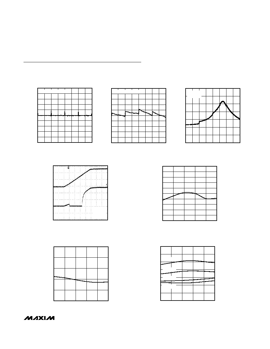
WIPER TRANSIENT AT POWER-ON
MAX5417 toc04
W
1V/div
V
DD
2V/div
4
µs/div
C
L
= 10pF
TAP = 128
H = V
DD
END-TO-END RESISTANCE % CHANGE
vs. TEMPERATURE
MAX5417 toc05
TEMPERATURE (
∞C)
END-TO-END RESISTANCE % CHANGE
60
35
10
-15
-0.8
-0.6
-0.4
-0.2
0
0.2
0.4
0.6
0.8
1.0
-1.0
-40
85
DNL vs. TAP POSITION
MAX5417 toc01
TAP POSITION
RESISTANCE DNL (LSB)
224
192
160
128
96
64
32
-0.20
-0.15
-0.10
-0.05
0
0.10
0.20
0.05
0.15
0.25
-0.25
0
256
VOLTAGE-DIVIDER MODE
TAP POSITION
RESISTANCE INL (LSB)
224
192
160
128
96
64
32
-0.20
-0.15
-0.10
-0.05
0
0.10
0.20
0.05
0.15
0.25
-0.25
0
256
INL vs. TAP POSITION
MAX5417 toc02
VOLTAGE-DIVIDER MODE
WIPER RESISTANCE vs. TAP POSITION
MAX5417 toc03
TAP POSITION
RESISTANCE (
)
224
192
160
128
96
64
32
100
200
300
400
500
600
700
0
0
256
V
DD
= 2.7V
I
SRC
= 50
µA
Typical Operating Characteristics
(V
DD
= +5V, T
A
= +25∞C, unless otherwise noted.)
STANDBY SUPPLY CURRENT
vs. TEMPERATURE
MAX5417 toc06
TEMPERATURE (
∞C)
STANDBY SUPPLY CURRENT (
µ
A)
60
35
10
-15
0.2
0.4
0.6
0.8
1.0
0
-40
85
WIPER RESISTANCE vs. TEMPERATURE
MAX5417 toc07
TEMPERATURE (
∞C)
RESISTANCE (
)
60
35
10
-15
100
200
300
400
500
600
700
0
-40
85
V
DD
= 2.7V
V
DD
= 3.0V
V
DD
= 4.5V
V
DD
= 5.25V