 | –≠–ª–µ–∫—Ç—Ä–æ–Ω–Ω—ã–π –∫–æ–º–ø–æ–Ω–µ–Ω—Ç: MAX5408 | –°–∫–∞—á–∞—Ç—å:  PDF PDF  ZIP ZIP |
General Description
The MAX5408≠MAX5411 dual, logarithmic taper digital
potentiometers, with 32-tap points each, replace
mechanical potentiometers in audio applications requir-
ing digitally controlled resistors. The MAX5408/
MAX5410 are dual potentiometers with one wiper per
potentiometer. The MAX5409/MAX5411 are dual poten-
tiometers with two wipers per potentiometer (see
Functional Diagram). An SPITM-compatible serial inter-
face controls the wiper positions. The MAX5408≠
MAX5411 have a factory-set resistance of 10k
per
potentiometer. A zero-crossing detect feature mini-
mizes the audible noise generated by wiper transitions.
The MAX5408≠MAX5411 have nominal temperature
coefficients of 35ppm/∞C end-to-end and 5ppm/∞C
ratiometric. The MAX5408≠MAX5411 are available in
16-pin QSOP and 16-pin thin QFN packages and are
specified over the extended temperature range (-40∞C
to +85∞C).
Applications
Stereo Volume Control
Fading and Balancing Stereo Signals
Mechanical Potentiometer Replacement
Features
o Log Taper with 2dB Steps Between Taps
o 32-Tap Positions for Each Wiper
o Small 16-Pin QSOP/QFN Packages
o Single-Supply Voltage Operation
+2.7V to +3.6V (MAX5408/MAX5409)
+4.5V to +5.5V (MAX5410/MAX5411)
o Low 0.5µA Standby Supply Current
o Zero-Crossing Detection for Clickless Switching
o Mute Function to -90dB
o 10k Fixed Resistance Value
o 3-Wire SPI-Compatible Serial Data Interface
o Power-On Reset: Wiper Goes to Maximum
Attenuation
o Digital Output for Readback and Daisy-Chaining
Capabilities
MAX5408≠MAX5411
Dual, Audio, Log Taper Digital Potentiometers
________________________________________________________________ Maxim Integrated Products
1
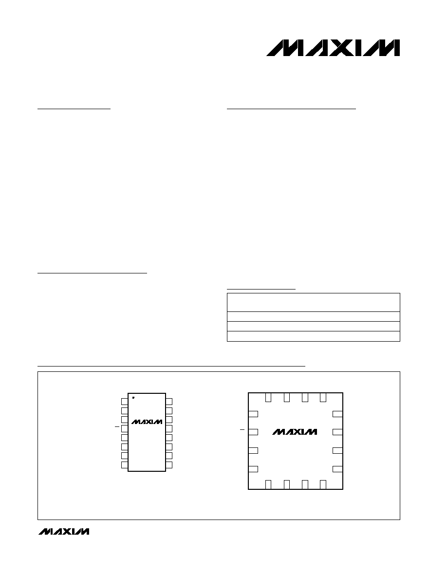
Pin Configurations
Ordering Information
19-2049; Rev 2; 9/02
For pricing, delivery, and ordering information, please contact Maxim/Dallas Direct! at
1-888-629-4642, or visit Maxim's website at www.maxim-ic.com.
PART
TEMP RANGE
PIN-
PACKAGE
WIPERS PER
RESISTOR
MAX5408EEE -40
∞C to +85∞C 16 QSOP
1
MAX5408ETE
-40
∞C to +85∞C 16 Thin QFN
1
MAX5409EEE -40
∞C to +85∞C 16 QSOP
2
16
15
14
13
12
11
10
9
1
2
3
4
5
6
7
8
DOUT
V
DD
V
LOGIC
GND
AGND
H1
L1
W1A
N.C. (W1B)
TOP VIEW
MAX5408-
MAX5411
QSOP
DIN
SCLK
L0
CS
H0
W0A
N.C. (W0B)
16
15
14
13
DIN
DOUT
V
DD
V
LOGIC
5
6
7
8
W0A
N.C. (W0B) N.C. (W1B)
W1A
9
10
11
12
L1
( ) ARE FOR MAX5409/MAX5411 ONLY
H1
AGND
GND
4
3
2
1
L0
H0
CS
SCLK
MAX5408-
MAX5411
THIN QFN
(4mm x 4mm)
(5mm x 6mm)
Ordering Information continued at end of data sheet.
Functional Diagram appears at end of data sheet.
SPI is a trademark of Motorola, Inc.

V
DD
, V
LOGIC
, CS, SCLK, DIN to GND ......................-0.3V to +6V
H_, L_, and W_ to GND ..............................-0.3V to (V
DD
+ 0.3V)
DOUT to GND.............................................-0.3V to (V
DD
+ 0.3V)
AGND to GND .......................................................-0.3V to +0.3V
Input and Output Latchup Immunity...............................±200mA
Maximum Continuous Current into H_, L_, and W_.........±500µA
Continuous Power Dissipation (T
A
= +70∞C)
16-Pin QSOP (derate 8.3mW/∞C above +70∞C)........666.7mW
16-Pin QFN (derate 18.5mW/∞C above +70∞C) .........1481mW
Operating Temperature Range ...........................-40∞C to +85∞C
Storage Temperature Range .............................-60∞C to +150∞C
Maximum Junction Temperature .....................................+150∞C
Lead Temperature (soldering, 10s) .................................+300∞C
MAX5408≠MAX5411
Dual, Audio, Log Taper Digital Potentiometers
2
_______________________________________________________________________________________
ABSOLUTE MAXIMUM RATINGS
ELECTRICAL CHARACTERISTICS
(V
DD
= +2.7V to +3.6V (MAX5408/MAX5409), V
DD
= +4.5V to +5.5V (MAX5410/MAX5411), V
H_
= V
DD
, V
L_
= 0, T
A
= T
MIN
to T
MAX
.
Typical values are at T
A
= +25∞C, unless otherwise specified.)
Stresses beyond those listed under "Absolute Maximum Ratings" may cause permanent damage to the device. These are stress ratings only, and functional
operation of the device at these or any other conditions beyond those indicated in the operational sections of the specifications is not implied. Exposure to
absolute maximum rating conditions for extended periods may affect device reliability.
PARAMETER
SYMBOL
CONDITIONS
MIN
TYP
MAX
UNITS
End-to-End Resistance
7
10
13
k
Maximum Bandwidth
(Note 1) C
W_
= 50pF
100
kHz
Absolute Tolerance
±0.25
dB
Tap-to-Tap Tolerance
±0.1
dB
Total Harmonic Distortion + Noise
THD+N
V
IN
= 1V
RMS
, f = 1kHz, tap = -6dB
0.002
%
Channel Isolation
-100
dB
Interchannel Matching
f = 20Hz to 20kHz, tap = -6dB
±0.5
dB
Mute Attenuation
-90
dB
Power-Supply Rejection Ratio
PSRR
-80
dB
Wiper Resistance
R
W
1000
1700
Wiper Capacitance
C
W
10
pF
Digital Clock Feedthrough
f
SCLK
= 20Hz to 20kHz, tap = -6dB
-90
dB
End-to-End Resistance
Temperature Coefficient
35
ppm/∞C
Ratiometric Resistance
Temperature Coefficient
5
ppm/∞C
DIGITAL INPUTS (V
LOGIC
> 4.5V)
Input High Voltage
V
IH
2.4
V
Input Low Voltage
V
IL
0.8
V
Input Leakage Current
±1
µA
Input Capacitance
5
pF
DIGITAL INPUTS (V
LOGIC
< 4.5V)
Input High Voltage
V
IH
0.7 x
V
LOGIC
V
Input Low Voltage
V
IL
0. 3 x
V
LOGIC
V
Input Leakage Current
±1
µA
Input Capacitance
5
pF
MAX5408≠MAX5411
Dual, Audio, Log Taper Digital Potentiometers
_______________________________________________________________________________________
3
ELECTRICAL CHARACTERISTICS (continued)
(V
DD
= +2.7V to +3.6V (MAX5408/MAX5409), V
DD
= +4.5V to +5.5V (MAX5410/MAX5411), V
H_
= V
DD
, V
L_
= 0, T
A
= T
MIN
to T
MAX
.
Typical values are at T
A
= +25∞C, unless otherwise specified.)
PARAMETER
SYMBOL
CONDITIONS
MIN
TYP
MAX
UNITS
DIGITAL OUTPUT
Output High Voltage
V
OH
I
SOURCE
= 0.5mA
V
LOGIC
- 0.5
V
Output Low Voltage
V
OL
I
SINK
= 2mA
0.4
V
TIMING CHARACTERISTICS (Figure 1)
SCLK Clock Period
t
CP
100
ns
SCLK Pulse Width High
t
CH
40
ns
SCLK Pulse Width Low
t
CL
40
ns
CS Fall to SCLK Rise Setup
Time
t
CSS
40
ns
SCLK Rise to CS Rise Hold Time
t
CSH
0
ns
DIN Setup Time
t
DS
40
ns
DIN Hold Time
t
DH
0
ns
SCLK Fall to DOUT Valid
Propagation Delay
t
DO
C
LOAD
= 200pF
80
ns
CS Rise to SCLK Rise Hold Time
t
CS1
40
ns
CS Pulse Width High
t
CSW
100
ns
Wiper Settling Time
t
IW
Zero-crossing detect disabled
1
µs
POWER SUPPLIES
MAX5408/MAX5409
2.7
3.6
Supply Voltage
V
DD
MAX5410/MAX5411
4.5
5.5
V
Active Supply Current
f
SCLK
= 2MHz (Note 2)
100
Standby Supply Current
I
DD
(Note 3)
0.2
10
µA
Logic Supply Voltage
V
LOGIC
2.7
5.5
V
Logic Active Supply Current
f
S C L K
= 2M H z, D OU T = fl oati ng ( N ote 2)
120
Logic Standby Supply Current
I
LOGIC
DOUT = floating (Note 3)
0.5
10
µA
Note 1: Guaranteed by design, not production tested.
Note 2: Supply current measured while changing wiper position with zero crossing enabled.
Note 3: Supply current measured while wiper position is fixed.
MAX5408≠MAX5411
Dual, Audio, Log Taper Digital Potentiometers
4
_______________________________________________________________________________________
Typical Operating Characteristics
(V
DD
= +3V (MAX5408/MAX5409), V
DD
= +5V (MAX5410/MAX5411), DOUT = floating)
988
990
989
991
994
995
993
992
996
0
1.0 1.5 2.0 2.5
0.5
3.0 3.5 4.0 4.5 5.0
WIPER RESISTANCE vs.
WIPER VOLTAGE
MAX5408-11
toc01
WIPER VOLTAGE (V)
WIPER RESISTANCE (
)
TAP POSITION 31
V
DD
= 5V = V
LOGIC
, L_ = GND
-0.20
-0.15
-0.10
-0.05
0
0.05
0.10
0.15
0.20
-40
-15
10
35
60
85
END-TO-END RESISTANCE % CHANGE
vs. TEMPERATURE
MAX5408-11 toc02
TEMPERATURE (
∞C)
END-TO-END RESISTANCE CHANGE (%)
-70
-60
-40
-50
-20
-10
-30
0
0
8
12
4
16
20
24
28
32
ATTENUATION vs. TAP POSITION
MAX5408-11 toc03
TAP POSITION
ATTENUATION (dB)
20
25
30
35
40
45
50
55
60
-40
-15
10
35
60
85
TOTAL SUPPLY CURRENT
VS.
TEMPERATURE
MAX5408-11 toc04
TEMPERATURE (
∞C)
TOTAL SUPPLY CURRENT (
µ
A)
ZERO-CROSSING ENABLED
I
TOTAL
= I
DD
+ I
LOGIC
ACTIVE MODE
4
µs/div
TAP-TO-TAP SWITCHING TRANSIENT
(ZERO-CROSSING DISABLE)
V
W_
2V/div
CS
2V/div
MAX5408-11 toc05
V
H
_ = 5V
V
L
_ = 0
0
0.10
0.05
0.20
0.15
0.25
0.30
2.5
3.5
4.0
3.0
4.5
5.0
5.5
LOGIC CURRENT
vs. LOGIC VOLTAGE
MAX5408-11 toc06
LOGIC SUPPLY VOLTAGE (V)
LOGIC SUPPLY CURRENT (
µ
A)
STANDBY MODE
SCLK = GND

MAX5408≠MAX5411
Dual, Audio, Log Taper Digital Potentiometers
_______________________________________________________________________________________
5
Typical Operating Characteristics (continued)
(V
DD
= +3V (MAX5408/MAX5409), V
DD
= +5V (MAX5410/MAX5411), DOUT = floating)
0
15
10
5
20
25
30
35
40
45
50
2.5
3.5
3.0
4.0
4.5
5.0
5.5
LOGIC CURRENT
vs. LOGIC VOLTAGE
MAX5408-11 toc07
LOGIC SUPPLY VOLTAGE (V)
LOGIC SUPPLY CURRENT (
µ
A)
ACTIVE MODE
SCLK = 2MHz, O to V
LOGIC
0
0.05
0.10
0.15
0.20
0.25
0.30
0.35
0.40
0.45
0.50
0.55
2.5
3.0
3.5
4.0
4.5
5.0
5.5
SUPPLY CURRENT
vs. SUPPLY VOLTAGE
MAX5408-11 toc08
V
DD
(V)
I
DD
(
µ
A)
ZERO-CROSSING DETECTION DISABLED
ACTIVE
STANDBY
Pin Description
PIN
M A X5 4 0 8 /
M A X5 4 1 0 ( Q F N )
M A X5 4 0 8 /
M A X5 4 1 0 ( Q SO P)
M A X5 4 0 9 /
M A X5 4 1 1 ( Q F N )
M A X5 4 0 9 /
M A X5 4 1 1 ( Q SO P)
NAME
FUNCTION
1
3
1
3
SCLK
Serial Clock Input
2
4
2
4
CS
Chip-Select Input
3
5
3
5
H0
High Terminal of Resistor 0
4
6
4
6
L0
Low Terminal of Resistor 0
5
7
5
7
W0A
Wiper Terminal A of Resistor 0
--
--
6
8
W0B
Wiper Terminal B of Resistor 0
--
--
7
9
W1B
Wiper Terminal B of Resistor 1
8
10
8
10
W1A
Wiper Terminal A of Resistor 1
9
11
9
11
L1
Low Terminal of Resistor 1
10
12
10
12
H1
High Terminal of Resistor 1
11
13
11
13
AGND
Analog Ground
12
14
12
14
GND
Ground
13
15
13
15
V
LOGIC
Digital Logic Power Supply
14
16
14
16
V
DD
Analog Power Supply
15
1
15
1
DOUT
Serial Data Output
16
2
16
2
DIN
Serial Data Input
6, 7
8, 9
--
--
N.C.
No Connection. Not internally connected.