 | –≠–ª–µ–∫—Ç—Ä–æ–Ω–Ω—ã–π –∫–æ–º–ø–æ–Ω–µ–Ω—Ç: MAX5352 | –°–∫–∞—á–∞—Ç—å:  PDF PDF  ZIP ZIP |
__________________General Description
The MAX5352/MAX5353 combine a low-power, voltage-
output, 12-bit digital-to-analog converter (DAC) and a
precision output amplifier in an 8-pin µMAX or DIP pack-
age. The MAX5352 operates from a single +5V supply,
and the MAX5353 operates from a single +3.3V supply.
Both devices draw less than 280µA of supply current.
The output amplifier's inverting input is available to the
user, allowing specific gain configurations, remote
sensing, and high output current capability. This makes
the MAX5352/MAX5353 ideal for a wide range of appli-
cations, including industrial process control. Other fea-
tures include a software shutdown and power-on reset.
The serial interface is compatible with SPITM/QSPITM
and MicrowireTM. The DAC has a double-buffered input,
organized as an input register followed by a DAC regis-
ter. A 16-bit serial word loads data into the input regis-
ter. The DAC register can be updated independently or
simultaneously with the input register. All logic inputs
are TTL/CMOS-logic compatible and buffered with
Schmitt triggers to allow direct interfacing to opto-
couplers.
________________________Applications
Industrial Process Controls
Automatic Test Equipment
Digital Offset and Gain Adjustment
Motion Control
Remote Industrial Controls
Microprocessor-Controlled Systems
______________________________Features
o
12-Bit DAC with Configurable Output Amplifier
o
+5V Single-Supply Operation (MAX5352)
+3.3V Single-Supply Operation (MAX5353)
o
Low Supply Current: 0.28mA Normal Operation
2µA Shutdown Mode
o
Available in 8-Pin µMAX
o
Power-On Reset Clears DAC Output to Zero
o
SPI/QSPI and Microwire Compatible
o
Schmitt-Trigger Digital Inputs for Direct
Optocoupler Interface
o
+3.3V MAX5353 Directly Interfaces with +5V Logic
MAX5352/MAX5353
Low-Power, 12-Bit Voltage-Output DACs
with Serial Interface
________________________________________________________________
Maxim Integrated Products
1
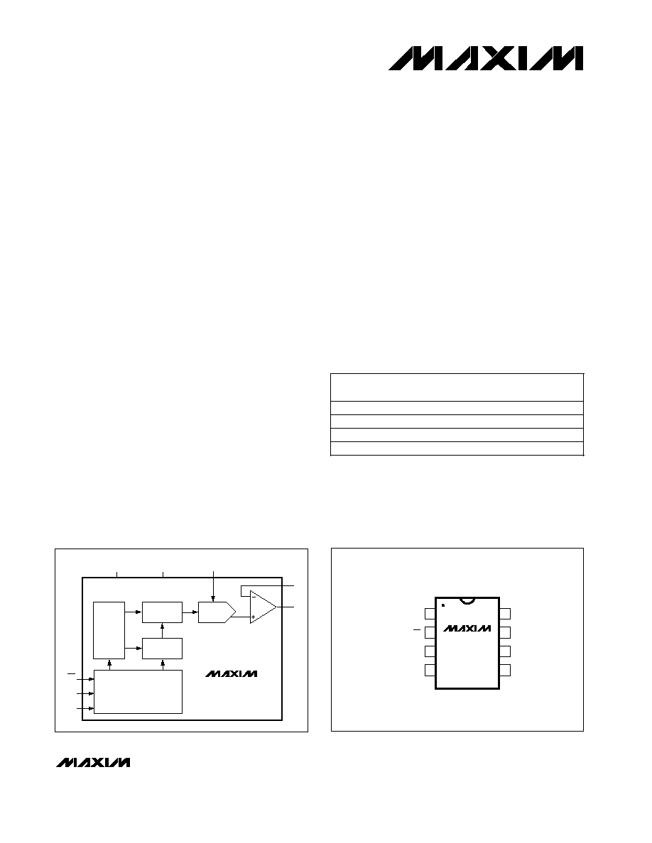
MAX5352
MAX5353
OUT
FB
CS
DIN
SCLK
DAC
REF
DAC
REGISTER
INPUT
REGISTER
CONTROL
V
DD
GND
16-BIT
SHIFT
REGISTER
____________________Functional Diagram
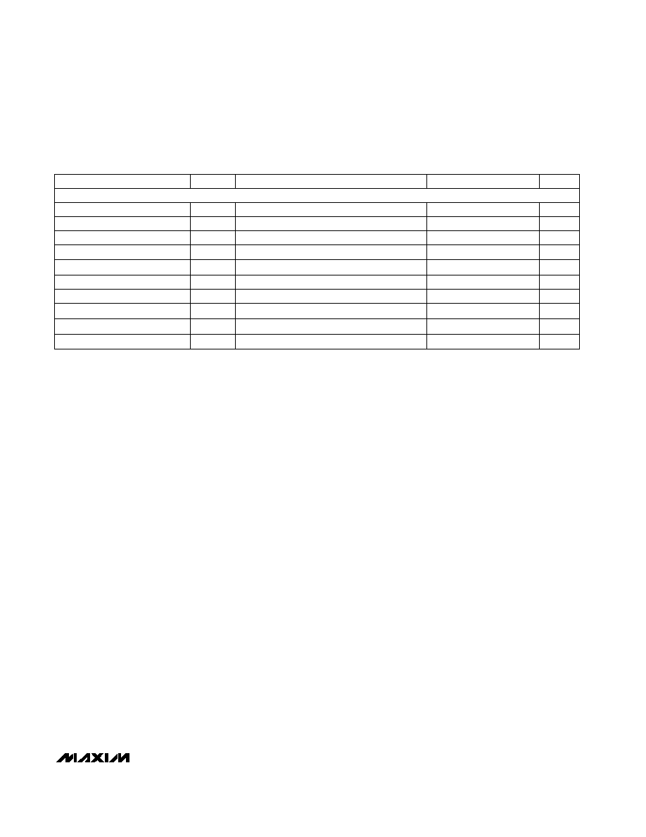
REF
DIN
FB
SCLK
1
2
8
7
V
DD
GND
CS
OUT
MAX5352
MAX5353
DIP/
µ
MAX
TOP VIEW
3
4
6
5
_______________________Pin Configuration
19-1196; Rev 0; 2/97
PART*
MAX5352
ACPA
MAX5352BCPA
0∞C to +70∞C
0∞C to +70∞C
TEMP. RANGE
PIN-PACKAGE
8 Plastic DIP
8 Plastic DIP
_________________Ordering Information
Ordering Information continued at end of data sheet.
*
Contact factory for availability of 8-pin SO package.
For free samples & the latest literature: http://www.maxim-ic.com, or phone 1-800-998-8800
INL
(LSB)
±1/2
±1
SPI and QSPI are registered trademarks of Motorola, Inc. Microwire is a registered trademark of National Semiconductor Corp.
MAX5352ACUA
MAX5352BCUA
0∞C to +70∞C
0∞C to +70∞C
8 µMAX
8 µMAX
±1/2
±1

MAX5352/MAX5353
Low-Power, 12-Bit Voltage-Output DACs
with Serial Interface
2
_______________________________________________________________________________________
ABSOLUTE MAXIMUM RATINGS
ELECTRICAL CHARACTERISTICS: MAX5352
(V
DD
= +5V ±10%, REF = 2.5V, GND = 0V, R
L
= 5k
, C
L
= 100pF, T
A
= T
MIN
to T
MAX
, unless otherwise noted. Typical values are at
T
A
= +25∞C. Output buffer connected in unity-gain configuration (Figure 8).)
Stresses beyond those listed under "Absolute Maximum Ratings" may cause permanent damage to the device. These are stress ratings only, and functional
operation of the device at these or any other conditions beyond those indicated in the operational sections of the specifications is not implied. Exposure to
absolute maximum rating conditions for extended periods may affect device reliability.
V
DD
to GND .................................................................-0.3V, +6V
REF, OUT, FB to GND ................................-0.3V to (V
DD
+ 0.3V)
Digital Inputs to GND ...............................................-0.3V to +6V
Continuous Current into Any Pin.......................................±20mA
Continuous Power Dissipation (T
A
= +70∞C)
Plastic DIP (derate 9.09mW/∞C above +70∞C) .................727mW
µMAX (derate 4.10mW/∞C above +70∞C) ......................330mW
CERDIP (derate 8.00mW/∞C above +70∞C) ...................640mW
Operating Temperature Ranges
MAX5352_C_A/MAX5353_C_A.............................0∞C to +70∞C
MAX5352_E_A/MAX5353_E_A ..........................-40∞C to +85∞C
MAX5352BMJA/MAX5353BMJA .....................-55∞C to +125∞C
Storage Temperature Range .............................-65∞C to +150∞C
Lead Temperature (soldering, 10sec) .............................+300∞C
Code dependent, minimum at code 1554 hex
4.5V
V
DD
5.5V
MAX5352BMJA
CONDITIONS
k
14
20
R
REF
Reference Input Resistance
V
0
V
DD
- 1.4
V
REF
Reference Input Range
µV/V
PSRR
Power-Supply Rejection Ratio
600
±0.5
Bits
12
N
Resolution
ppm/∞C
1
Gain-Error Tempco
LSB
GE
Gain Error (Note 1)
-0.3
±3
ppm/∞C
6
TCV
OS
Offset-Error Tempco
LSB
±1.0
INL
Integral Nonlinearity
(Note 1)
±2.0
±0.3
±8
mV
V
OS
Offset Error
UNITS
MIN
TYP
MAX
SYMBOL
PARAMETER
MAX5352A
MAX5352B
Guaranteed monotonic
LSB
±1.0
DNL
Differential Nonlinearity
V
REF
= 0.67Vp-p
kHz
650
Reference -3dB Bandwidth
Input code = all 0s, V
REF
= 3.6Vp-p at 1kHz
V
REF
= 1Vp-p at 25kHz, code = full scale
dB
77
SINAD
Signal-to-Noise Plus
Distortion Ratio
dB
-84
Reference Feedthrough
V
2.4
V
IH
Input High Voltage
V
IN
= 0V or V
DD
pF
8
C
IN
Input Capacitance
µA
0.001
±0.5
I
IN
Input Leakage Current
V
0.8
V
IL
Input Low Voltage
STATIC PERFORMANCE--ANALOG SECTION
DIGITAL INPUTS
REFERENCE INPUT
MULTIPLYING-MODE PERFORMANCE

MAX5352/MAX5353
Low-Power, 12-Bit Voltage-Output DACs
with Serial Interface
_______________________________________________________________________________________
3
ELECTRICAL CHARACTERISTICS: MAX5352 (continued)
(V
DD
= +5V ±10%, REF = 2.5V, GND = 0V, R
L
= 5k
, C
L
= 100pF, T
A
= T
MIN
to T
MAX
, unless otherwise noted. Typical values are at
T
A
= +25∞C. Output buffer connected in unity-gain configuration (Figure 8).)
(Note 3)
CS = V
DD
, DIN = 100kHz
Rail-to-rail (Note 2)
To ±1/2LSB, V
STEP
= 2.5V
CONDITIONS
mA
0.28
0.4
I
DD
Supply Current
V
4.5
5.5
V
DD
Supply Voltage
nV-s
5
Digital Feedthrough
µs
20
Start-Up Time
µA
0.001
±0.1
Current into FB
V
0 to V
DD
Output Voltage Swing
µs
14
Output Settling Time
V/µs
0.6
SR
Voltage Output Slew Rate
UNITS
MIN
TYP
MAX
SYMBOL
PARAMETER
(Note 3)
µA
4
20
Supply Current in Shutdown
µA
0.001
±0.5
Reference Current in Shutdown
ns
40
t
CH
SCLK Pulse Width High
ns
100
t
CP
SCLK Clock Period
ns
40
t
CSS
CS Fall to SCLK Rise Setup Time
ns
40
t
DS
DIN Setup Time
ns
0
t
CSH
SCLK Rise to CS Rise Hold Time
ns
40
t
CL
SCLK Pulse Width Low
ns
40
t
CS1
CS Rise to SCLK Rise Hold Time
ns
100
t
CSW
CS Pulse Width High
ns
40
t
CS0
SCLK Rise to CS Fall Delay
ns
0
t
DH
DIN Hold Time
Note 1:
Guaranteed from code 11 to code 4095 in unity-gain configuration.
Note 2:
Accuracy is better than 1LSB for V
OUT
= 8mV to V
DD
- 100mV, guaranteed by a power-supply rejection test at the
end points.
Note 3:
R
L
=
, digital inputs at GND or V
DD
.
DIGITAL INPUTS
DYNAMIC PERFORMANCE
POWER SUPPLIES
TIMING CHARACTERISTICS
(Figure 6)

MAX5352/MAX5353
Low-Power, 12-Bit Voltage-Output DACs
with Serial Interface
4
_______________________________________________________________________________________
ELECTRICAL CHARACTERISTICS: MAX5353
(V
DD
= +3.15V to +3.6V, REF = 1.25V, GND = 0V, R
L
= 5k
, C
L
= 100pF, T
A
= T
MIN
to T
MAX
, unless otherwise noted. Typical values
are at T
A
= +25∞C. Output buffer connected in unity-gain configuration (Figure 8).)
Guaranteed monotonic
LSB
Code dependent, minimum at code 1554 hex
±1.0
V
REF
= 0.67Vp-p
DNL
kHz
Differential Nonlinearity
650
MAX5353BMJA
Reference -3dB Bandwidth
CONDITIONS
Input code = all 0s, V
REF
= 1.9Vp-p at 1kHz
V
REF
= 1Vp-p at 25kHz, code = full scale
dB
72
k
14
20
R
REF
Reference Input Resistance
V
0
V
DD
- 1.4
V
REF
Reference Input Range
SINAD
Signal-to-Noise Plus
Distortion Ratio
dB
-84
Reference Feedthrough
V
2.4
V
IH
Input High Voltage
µV/V
PSRR
Power-Supply Rejection Ratio
600
V
IN
= 0V or V
DD
±1
MAX5353A
MAX5353B
Bits
12
N
Resolution
ppm/∞C
1
Gain-Error Tempco
LSB
GE
Gain Error (Note 4)
-0.3
±3
pF
ppm/∞C
6
TCV
OS
Offset-Error Tempco
LSB
±2
INL
Integral Nonlinearity
(Note 4)
8
±4
C
IN
Input Capacitance
µA
±0.3
±8
0.001
±0.5
I
IN
mV
Input Leakage Current
V
OS
Offset Error
UNITS
MIN
TYP
MAX
SYMBOL
PARAMETER
V
0.6
V
IL
Input Low Voltage
To ±1/2LSB, V
STEP
= 1.25V
Rail-to-rail (Note 5)
V
0 to V
DD
Output Voltage Swing
µs
14
Output Settling Time
V/µs
0.6
SR
Voltage Output Slew Rate
µA
0.001
±0.1
Current into FB
CS = V
DD
, DIN = 100kHz
V
3.15
3.6
V
DD
Supply Voltage
nV-s
5
Digital Feedthrough
(Note 6)
(Note 6)
µA
0.001
±0.5
Reference Current in Shutdown
µA
1.6
10
Supply Current in Shutdown
mA
0.24
0.4
I
DD
Supply Current
µs
20
Start-Up Time
STATIC PERFORMANCE--ANALOG SECTION
DIGITAL INPUTS
REFERENCE INPUT
MULTIPLYING-MODE PERFORMANCE
(V
DD
= +3.3V)
DYNAMIC PERFORMANCE
POWER SUPPLIES
MAX5352/MAX5353
Low-Power, 12-Bit Voltage-Output DACs
with Serial Interface
_______________________________________________________________________________________
5
ELECTRICAL CHARACTERISTICS: MAX5353 (continued)
(V
DD
= +3.15V to +3.6V, REF = 1.25V, GND = 0V, R
L
= 5k
, C
L
= 100pF, T
A
= T
MIN
to T
MAX
, unless otherwise noted. Typical values
are at T
A
= +25∞C. Output buffer connected in unity-gain configuration (Figure 8).)
ns
CONDITIONS
40
t
CH
SCLK Pulse Width High
ns
100
t
CP
SCLK Clock Period
ns
40
t
CSS
CS Fall to SCLK Rise Setup Time
ns
40
t
DS
DIN Setup Time
ns
0
t
CSH
SCLK Rise to CS Rise Hold Time
ns
40
t
CL
SCLK Pulse Width Low
UNITS
MIN
TYP
MAX
SYMBOL
PARAMETER
ns
40
t
CS1
CS Rise to SCLK Rise Hold Time
ns
0
t
DH
DIN Hold Time
ns
100
t
CSW
CS Pulse Width High
ns
40
t
CS0
SCLK Rise to CS Fall Delay
Note 4:
Guaranteed from code 22 to code 4095 in unity-gain configuration.
Note 5:
Accuracy is better than 1LSB for V
OUT
= 8mV to V
DD
- 150mV, guaranteed by a power-supply rejection test at the
end points.
Note 6:
R
L
=
, digital inputs at GND or V
DD
.
TIMING CHARACTERISTICS
(Figure 6)