 | –≠–ª–µ–∫—Ç—Ä–æ–Ω–Ω—ã–π –∫–æ–º–ø–æ–Ω–µ–Ω—Ç: MAX532 | –°–∫–∞—á–∞—Ç—å:  PDF PDF  ZIP ZIP |

_______________General Description
The MAX532 is a complete, dual, serial-input, 12-bit
multiplying digital-to-analog converter (MDAC) with out-
put amplifiers. No external user trims are required to
achieve full specified performance. The MAX532's 3-
wire serial interface minimizes the number of package
pins, so it uses less board space than parallel-interface
parts. The interface is SPITM, QSPITM and MicrowireTM
compatible. A serial output, DOUT, allows cascading
of two or more MAX532s and read-back of the data
written to the device.
The device's serial interface minimizes digital-noise
feedthrough from its logic pins to its analog outputs.
Serial interfacing also simplifies opto-coupler-isolated
or transformer-isolated applications.
The MAX532 is specified with ±12V to ±15V power sup-
plies. All logic inputs are TTL and CMOS compatible. It
comes in space-saving 16-pin DIP and wide SO packages.
________________________Applications
Automatic Test Equipment
Arbitrary Waveform Generators
Programmable-Gain Amplifiers
Motion Control Systems
Servo Controls
____________________________Features
o
Two 12-Bit MDACs with Output Amplifiers
o
Fast, 6MHz 3-Wire Interface
o
SPI, QSPI, and Microwire Compatible
o
±12V Output Swing
o
±10mA Output Current
o
2.5µs Settling Time to ±1/2LSB
o
Guaranteed Monotonic Over Temperature
o
Low Integral Nonlinearity: ±1/2LSB Max
o
Low Gain Tempco: 2ppm/∞C
o
Operates from ±12V to ±15V Supplies
o
Power-On Reset
o
Available in 16-Pin DIP and Wide SO Packages
______________Ordering Information
MAX532
Dual, Serial-Input,
Voltage-Output, 12-Bit MDAC
________________________________________________________________
Maxim Integrated Products
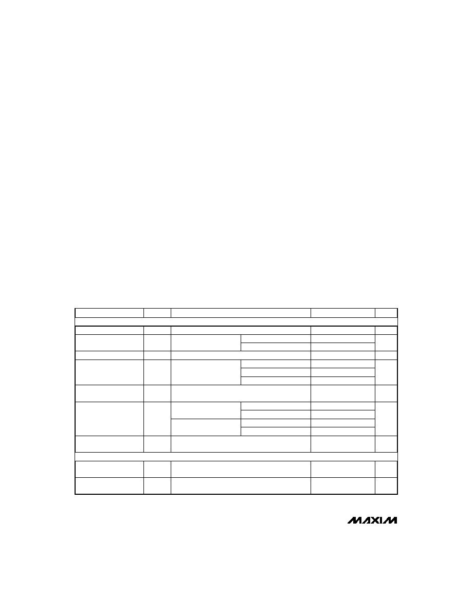
1
16
15
14
13
12
11
10
9
1
2
3
4
5
6
7
8
V
DD
LDAC
CS
DIN
AGNDA
VOUTA
VREFA
RFBA
TOP VIEW
DOUT
SCLK
DGND
V
SS
RFBB
VREFB
VOUTB
AGNDB
DIP/Wide SO
MAX532
__________________Pin Configuration
DACA
LATCH
24-BIT SHIFT
REGISTER
DACB
LATCH
DACA
RFBA
VOUTA
DOUT
RFBB
VOUTB
AGNDB
AGNDA
VREFA
DIN
SCLK
CS
LDAC
VREFB
DACB
V
DD
V
SS
DGND
MAX532
________________Functional Diagram
Call toll free 1-800-998-8800 for free samples or literature.
19-0046; Rev. 1; 3/94
PART
TEMP. RANGE PIN-PACKAGE
MAX532ACPE
0∞C to +70∞C
16 Plastic DIP
MAX532BCPE
0∞C to +70∞C
16 Plastic DIP
MAX532ACWE
0∞C to +70∞C
16 Wide SO
MAX532BCWE
0∞C to +70∞C
16 Wide SO
MAX532BC/D
0∞C to +70∞C
Dice*
TMMicrowire is a trademark of National Semiconductor Corp. SPI and QSPI are trademarks of Motorola, Inc.
±1/2
±1
±1/2
±1
±1
ERROR
(LSBs)
Ordering Information continued on last page.
* Contact factory for dice specifications.
MAX532
Dual, Serial-Input,
Voltage-Output, 12-Bit MDAC
2
_______________________________________________________________________________________
Pin Voltages
V
DD
to DGND, AGNDA, AGNDB........................-0.3V to +17V
V
SS
to DGND, AGNDA, AGNDB (Note 1) ..........+0.3V to -17V
VREFA, VREFB.............................(V
SS
- 0.3V) to (V
DD
+ 0.3V)
AGNDA, AGNDB .....................(DGND - 0.3V) to (V
DD
+ 0.3V)
VOUTA, VOUTB ...........................(V
SS
- 0.3V) to (V
DD
+ 0.3V)
RFBA, RFBB.................................(V
SS
- 0.3V) to (V
DD
+ 0.3V)
SCLK, DIN, DOUT,
LDAC, CS ..(DGND - 0.3V) to (V
DD
+ 0.3V)
DOUT Sink Current .............................................................20mA
Continuous Power Dissipation (T
A
= +70∞C)
Plastic DIP (derate 10.53mW/∞C above +70∞C) ..........842mW
Wide SO (derate 9.52mW/∞C above +70∞C)................762mW
CERDIP (derate 10.00mW/∞C above +70∞C) ...............800mW
Operating Temperature Ranges:
MAX532_C__ ......................................................0∞C to +70∞C
MAX532_E__....................................................-40∞C to +85∞C
MAX532_MJE ................................................-55∞C to +125∞C
Junction Temperatures:
MAX532_C__, E__........................................................+150∞C
MAX532_MJE...............................................................+175∞C
Storage Temperature Range ........................... -65∞C to +160∞C
Lead Temperature (soldering, 10sec) ........................... +300∞C
ELECTRICAL CHARACTERISTICS
(V
DD
= 11.4V to 16.5V, V
SS
= -11.4V to -16.5V, AGNDA = AGNDB = DGND = 0V, VREFA and VREFB = +10V, R
L
= 2k
,
C
L
= 100pF, VOUT_ connected to RFB_, T
A
= T
MIN
to T
MAX
, unless otherwise noted.)
Stresses beyond those listed under "Absolute Maximum Ratings" may cause permanent damage to the device. These are stress ratings only, and functional
operation of the device at these or any other conditions beyond those indicated in the operational sections of the specifications is not implied. Exposure to
absolute maximum rating conditions for extended periods may affect device reliability.
ABSOLUTE MAXIMUM RATINGS
PARAMETER
CONDITIONS
MIN
TYP
MAX
UNITS
SYMBOL
Resolution
INL
12
Bits
Relative Accuracy
±1
LSB
Differential Nonlinearity
Guaranteed monotonic
±1
LSB
±1/2
MAX532A
MAX532B
±2
T
A
= +25∞C, MAX532_
±3
Zero-Code Offset Error
DAC latch loaded
with all 0s
±4
mV
T
A
= T
MIN
to T
MAX
, MAX532B
±5
µV/∞C
DAC latch loaded with all 0s
±2
MAX532A
T
A
= +25∞C, DAC latch
loaded with all 1s
±5
MAX532B
±0.5
±3.0
%
8
10
13
k
±2
ppm/∞C
of FSR
Gain Error
T
A
= T
MIN
to T
MAX
, DAC
latch loaded with all 1s
±7
LSB
MAX532B
±4
MAX532A
T
A
= T
MIN
to T
MAX
, MAX532A
Zero-Code Offset
Temperature Coefficient
Gain-Error Temperature
Coefficient
VREFA, VREFB Input
Resistance
VREFA, VREFB Input
Resistance Matching
STATIC PERFORMANCE
(Note 1)
REFERENCE INPUTS (VREFA, VREFB)
Note 1:
If V
SS
is open-circuited with V
DD
and either AGND applied, the V
SS
pin will float positive, exceeding the Absolute Maximum Ratings.
A Schottky diode connected between V
SS
and GND ensures the maximum ratings will not be exceeded.

MAX532
Dual, Serial-Input,
Voltage-Output, 12-Bit MDAC
_______________________________________________________________________________________
3
ELECTRICAL CHARACTERISTICS (continued)
(V
DD
= 11.4V to 16.5V, V
SS
= -11.4V to -16.5V, AGNDA = AGNDB = DGND = 0V, VREFA and VREFB = +10V, R
L
= 2k
, C
L
= 100pF,
VOUT_ connected to RFB_, T
A
= T
MIN
to T
MAX
, unless otherwise noted.)
PARAMETER
CONDITIONS
MIN
TYP
MAX
UNITS
SYMBOL
V
INL
V
OL
Input Low Voltage
0.8
V
I
SINK
= 5mA
0.08
0.4
Output Voltage Low
I
SINK
= 16mA
0.2
V
V
INH
Input High Voltage
2.4
V
Input Current
Digital inputs at 0V or V
DD
±1
µA
8
pF
Input Capacitance (Note 2)
I
LKG
Output High Leakage
V
DOUT
= 0V to V
DD
±10
µA
C
OUT
15
pF
DC Output Impedance
0.2
Short-Circuit Current
VOUTA, VOUTB connected to AGNDA, AGNDB
20
mA
Output Voltage Swing
V
V
DD
Positive Supply Voltage
11.4
16.5
V
V
SS
Negative Supply Voltage
-11.4
-16.5
V
±0.035
PSR
Power-Supply Rejection
±0.035
LSB/%
I
DD
Positive Supply Current
Output unloaded
5
10
mA
I
SS
Negative Supply Current
Output unloaded
4
6
mA
Settling time to within 1/2 LSB of final DAC value; DAC
latch alternately loaded with all 0s and all 1s
2.5
µs
Slew Rate
8
V/µs
DAC latch alternately loaded with 011...11 and 100...00
60
nV-s
Output High Capacitance
(Note 2)
Full scale/
V
DD
, V
DD
= 11.4V to 16.5V, VREF = -8.9V,
DAC latches loaded with all 1s
Full scale/
V
SS
, V
SS
= -11.4V to -16.5V, VREF = 8.9V,
DAC latches loaded with all 1s
VREFA to VOUTB
-100
Channel-to-Channel
Isolation
VREFB to VOUTA
-100
dB
Voltage-Output
Settling Time
Digital-to-Analog
Glitch Impulse
VREFA = 20V
p-p
10kHz
sine wave; DAC latches
loaded with all 0s
VREFB = 20V
p-p
10kHz
sine wave; DAC latches
loaded with all 0s
(V
DD
- 2.5)
to
(V
SS
+ 2.5)
DIGITAL INPUTS (SCLK, DIN,
LDAC
,
CS
)
DIGITAL OUTPUT (DOUT)
(Note 3)
ANALOG OUTPUTS (VOUTA, VOUTB)
POWER REQUIREMENTS
AC CHARACTERISTICS
MAX532
Dual, Serial-Input,
Voltage-Output, 12-Bit MDAC
4
_______________________________________________________________________________________
ELECTRICAL CHARACTERISTICS (continued)
(V
DD
= 11.4V to 16.5V, V
SS
= -11.4V to -16.5V, AGNDA = AGNDB = DGND = 0V, VREFA and VREFB = +10V, R
L
= 2k
, C
L
= 100pF,
VOUT_ connected to RFB_, T
A
= T
MIN
to T
MAX
, unless otherwise noted.)
PARAMETER
CONDITIONS
MIN
TYP
MAX
UNITS
SYMBOL
VREF = 100mV
p-p
sine wave;
DAC latch loaded with all 1s
1.0
MHz
VREF = 20V
p-p
10kHz sine wave;
DAC latch loaded with all 0s
-77
dB
Full-Power Bandwidth
125
kHz
THD
Total Harmonic Distortion
-90
dB
Output Noise Voltage
0.1Hz to 10Hz
2
µV
RMS
Digital Crosstalk
DACA code all 1s, DACB code transition from all 0s to all 1s
10
nV-s
Digital Feedthrough
CS = 1; transitions on SCLK, LDAC, DIN
1.1
nV-s
PARAMETER
t
CL
CONDITIONS
MIN
TYP
MAX
SCLK Pulse Width Low
UNITS
SYMBOL
f
CLK
t
CH
80
ns
t
DS
50
ns
t
CSS1
CS Rise to SCLK Rise Setup Time
SCLK Clock Frequency
50
ns
t
CSS0
CS Fall to SCLK Rise Setup Time
6.25
MHz
50
ns
t
DH
DIN to SCLK Rise Hold Time
0
ns
SCLK Pulse Width High
80
ns
Multiplying Feedthrough
Error
Unity-Gain Small-Signal
Bandwidth
VREF = 20V
p-p
sine wave;
DAC latch loaded with all 1s
VREF = 6V
RMS
, 1kHz sine wave;
DAC latch loaded with all 1s
Note 1:
Static performance tested at V
DD
= +15V, V
SS
= -15V. Performance over supplies guaranteed by PSR test.
Note 2:
Guaranteed by design. Not subject to production testing.
Note 3:
Open-drain output.
TIMING CHARACTERISTICS
(V
DD
= 11.4V to 16.5V, V
SS
= -11.4V to -16.5V, AGNDA = AGNDB = DGND = 0V) (Notes 4, 5)
t
CSH0
SCLK Fall to
CS Fall Hold Time
5
ns
t
CSH1
SCLK Rise to
CS Rise Hold Time
80
ns
t
CSW
CS Pulse Width High
120
ns
t
DO
SCLK Fall to DOUT Valid (Note 6)
C
L
= 20pF, R
PULL-UP
= 1k
to 5V
0
200
ns
t
DV
CS Fall to DOUT Enable (Note 7)
C
L
= 20pF, R
PULL-UP
= 1k
to 5V
100
ns
t
TR
CS Rise to DOUT Disable (Note 7)
C
L
= 20pF, R
PULL-UP
= 1k
to 5V
60
ns
t
LDAC
LDAC Pulse Width Low
60
ns
t
LDACS
CS Rise to LDAC Fall Setup Time
100
ns
DIN to SCLK Rise Setup Time
Note 4:
All input signals are specified with t
R
= t
F
5ns. Logic input swing is 0V to 5V.
Note 5:
See Figure 1.
Note 6:
Timing is for SCLK fall to DOUT fall to 0.8V, or for SCLK fall to DOUT rise to 2.4V. Additional time must be added for any
larger passive RC pull-up delay.
Note 7:
DOUT enable: DOUT falls to 4.5V from 5.0V. DOUT disable: DOUT rises to 0.5V from 0V.

MAX532
Dual, Serial-Input,
Voltage-Output, 12-Bit MDAC
_________________________________________________________________________________________________
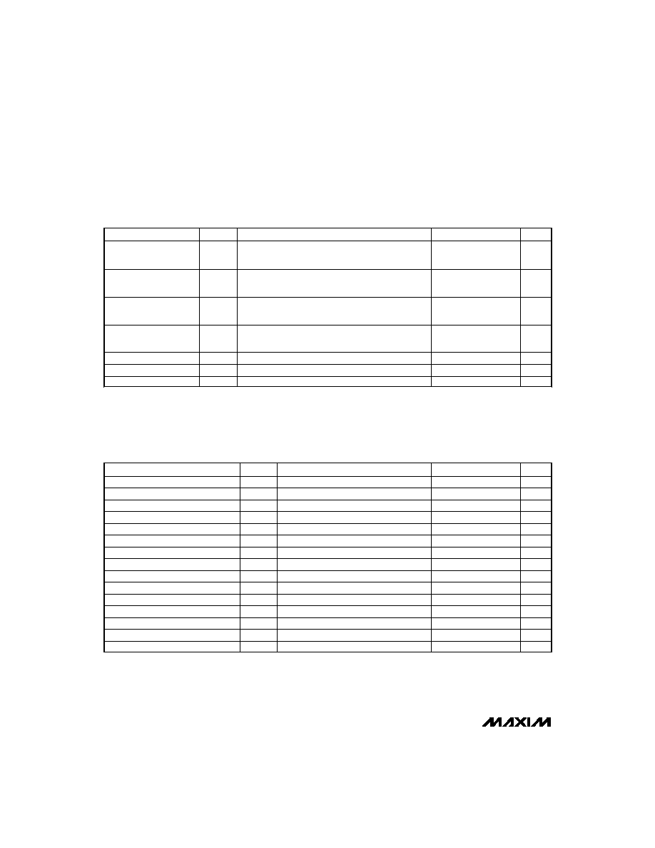
5
25
0
10
1k
10k
OUTPUT VOLTAGE SWING
vs. RESISTIVE LOAD
10
20
LOAD RESISTANCE (
)
V
OUT
(V
p-p
)
100
15
5
VREF = 20V
p-p
at 1kHz
0
10
100k
NOISE SPECTRAL DENSITY
100
300
FREQUENCY (Hz)
NOISE SPECTRAL DENSITY (nV Hz)
200
100
1k
10k
VREF = 0V
DAC CODE = 11...111
GAIN = -1
5
-40
100
10k
10M
LARGE-SIGNAL FREQUENCY RESPONSE
FREQUENCY (Hz)
GAIN (dB)
-5
0
-10
-15
-30
1k
100k
1M
VREF = 20Vp-p
DAC CODE = 11...111
GAIN = -1
-20
-25
-35
5
-25
100
10k
10M
SMALL-SIGNAL FREQUENCY RESPONSE
FREQUENCY (Hz)
GAIN (dB)
-5
0
-10
-15
-20
1k
100k
1M
VREF = 100mV
p-p
DAC CODE = 11...111
-35
-85
1k
100k
MULTIPLYING FEEDTHROUGH ERROR
-75
FREQUENCY (Hz)
ATTENUATION (dB)
-65
-50
-45
-40
-55
-60
-70
-80
10k
1M
VREFA = 20V
p-p
VREFB = AGNDB
DAC CODE = 00...00
-94
-106
100
1k
10k
TOTAL HARMONIC DISTORTION + NOISE
vs. FREQUENCY (BANDWIDTH = 80kHz)
-102
FREQUENCY (Hz)
THD (dB)
-100
-98
-96
-104
VREF = 6V
RMS
DAC CODE = 111...111
-60
-100
100
10k
100k
TOTAL HARMONIC DISTORTION + NOISE
vs. FREQUENCY (BANDWIDTH > 500kHz)
-75
-65
FREQUENCY (Hz)
THD (dB)
1k
-70
-90
-80
-85
-95
VREF = 6V
RMS
DAC CODE = 111...111
__________________________________________Typical Operating Characteristics
(V
DD
= 15V, V
SS
= -15V, R
L
= 2k
, C
L
= 100pF, unless otherwise noted.)