 | –≠–ª–µ–∫—Ç—Ä–æ–Ω–Ω—ã–π –∫–æ–º–ø–æ–Ω–µ–Ω—Ç: MAX5168 | –°–∫–∞—á–∞—Ç—å:  PDF PDF  ZIP ZIP |
General Description
The MAX5168 contains 32 sample/hold amplifiers and
four 1-of-8 multiplexers. The logic controlling the muxes
and sample/hold amplifiers combines the four muxes into
a unified 1-of-32 multiplexer with a sample/hold at each
output. Additional logic allows two devices to function as
a single 64-channel unit. The MAX5168 is available with
an output impedance of 50
, 500, or 1k.
The MAX5168 operates with +10V and -5V supplies, and
a separate +5V digital logic supply. Manufactured with a
proprietary BiCMOS process, it provides high accuracy,
fast acquisition time, a low droop rate, and a low hold
step. The MAX5168 has a typical linearity error of less
than 0.01% and can accurately acquire 8V step input sig-
nals to 0.01% accuracy in 2.5µs within the +7V to -4V
input signal range. Transitions from sample mode to hold
mode result in only a 0.5mV error. While in hold mode, the
output voltage slowly droops at a rate of 1mV/s.
The MAX5168 is available in a 48-pin TQFP package and
is specified for both the commercial (0∞C to +70∞C) and
extended industrial (-40∞C to +85∞C) temperature ranges.
________________________Applications
Automatic Test Systems (ATE)
Industrial Process Controls
Arbitrary Function Generators
Avionics Equipment
Features
o 32-Channel Sample/Hold
o 0.01% Accuracy of Acquired Signal
o 0.01% Linearity Error
o Fast Acquisition Time: 2.5µs
o Low Droop Rate: 1mV/s
o Low Hold Step: 0.25mV
o Wide Output Voltage Range: +7V to -4V
MAX5168
32-Channel Sample/Hold Amplifier
with a Single Multiplexed Input
________________________________________________________________ Maxim Integrated Products
1
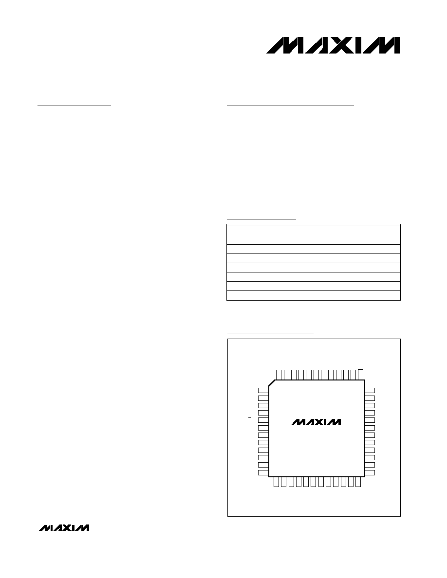
OUT21
OUT20
OUT19
OUT18
OUT17
OUT16
V
DD
OUT15
OUT14
OUT13
OUT12
OUT11
ADDR2
ADDR3
ADDR4
SELECT
S/H
CONFIG
V
L
DGND
V
SS
AGND
IN
N.C.
1
2
3
4
5
6
7
8
9
10
11
12
13
14
15
16
17
18
19
20
21
22
23
24
48
47
46
45
44
43
42
41
40
39
38
37
36
35
34
33
32
31
30
29
28
27
26
25
N.C.
OUT0
OUT1
OUT2
OUT3
OUT4
OUT5
OUT6
OUT7
OUT8
OUT9
OUT10
ADDR1
ADDR0
OUT31
OUT30
OUT29
OUT28
OUT27
OUT26
OUT25
OUT24
OUT23
OUT22
TQFP
MAX5168
TOP VIEW
Pin Configuration
19-1674; Rev 0; 4/00
Ordering Information
48 TQFP
PIN-
PACKAGE
TEMP. RANGE
0∞C to +70∞C
MAX5168LCCM
PART
48 TQFP
0∞C to +70∞C
MAX5168MCCM
48 TQFP
0∞C to +70∞C
MAX5168NCCM
48 TQFP
-40∞C to +85∞C
MAX5168LECM
48 TQFP
-40∞C to +85∞C
MAX5168MECM
48 TQFP
-40∞C to +85∞C
MAX5168NECM
50
R
OUT
(
)
500
1k
50
500
1k
For free samples and the latest literature, visit www.maxim-ic.com or phone 1-800-998-8800.
For small orders, phone 1-800-835-8769.

IN = AGND, T
A
=
MAX5168
32-Channel Sample/Hold Amplifier
with a Single Multiplexed Input
2
_______________________________________________________________________________________
ABSOLUTE MAXIMUM RATINGS
ELECTRICAL CHARACTERISTICS
(V
DD
= +10.0V, V
SS
= -5.0V, V
L
= +5.0V ±5%, AGND = DGND = 0, R
L
= 5k
, C
L
= 50pF, T
A
= T
MIN
to T
MAX
, unless otherwise noted.
Typical values are at T
A
= +25∞C.)
Stresses beyond those listed under "Absolute Maximum Ratings" may cause permanent damage to the device. These are stress ratings only, and functional
operation of the device at these or any other conditions beyond those indicated in the operational sections of the specifications is not implied. Exposure to
absolute maximum rating conditions for extended periods may affect device reliability.
V
DD
to AGND.......................................................-0.3V to +11.0V
V
SS
to AGND .........................................................-6.0V to +0.3V
V
DD
to V
SS
......................................................................+15.75V
V
L
to DGND ...........................................................-0.3V to +6.0V
V
L
to AGND ...........................................................-0.3V to +6.0V
DGND to AGND.....................................................-0.3V to +2.0V
IN, OUT_ .....................................................................V
SS
to V
DD
Logic Inputs to DGND ...........................................-0.3V to +6.0V
Maximum Current into OUT_ ............................................±10mA
Maximum Current into Logic Inputs .................................±20mA
Continuous Power Dissipation (T
A
= +70∞C)
48-Pin TQFP (derate 12.5mW/∞C above +70∞C)......1000mW
Operating Temperature Ranges
MAX5168_CCM ................................................0∞C to +70∞C
MAX5168_ECM..............................................-40∞C to +85∞C
Storage Temperature Range .............................-65∞C to +150∞C
Lead Temperature (soldering, 10s) .................................+300∞C
Figure 2 (Note 1)
IN = AGND
To ±1mV of final value, Figure 2 (Note 1)
-4.0V < V
IN
< +7V, R
L
=
T
A
= +25∞C,
R
L
=
, Figure 2
R
L
=
,
C
L
= 250pF
(Note 1)
V
IN
= 0, sample mode
V
IN
= 0, sample mode
8V step with 500ns
rising edge (Note 1)
MAX5168N
+15∞C
T
A
+65∞C (Note 1)
8V step to 0.08%
R
L
=
100mV step to ±1mV
CONDITIONS
ns
200
t
AP
Aperture Delay
µs
1
2
t
H
Hold-Mode Settling Time
1
µs
2.5
4
t
AQ
Acquisition Time
V
V
SS
V
DD
V
CH
Output Clamp High
mA
2
I
SINK
Output Sink Current
mA
2
I
SOURCE
Output Source Current
700
1000
1300
350
500
650
R
OUT_
mV
0.25
1.00
V
HS
Hold Step
%
0.01
0.08
Linearity Error
35
50
65
DC Output Impedance
pF
10
20
C
IN
Input Capacitance
MAX5168M
-72
-76
MAX5168L
dB
-72
-76
Analog Crosstalk
mV/s
1
40
Droop Rate
mV
-30
-5
+30
V
OS
Offset Voltage
µV/∞C
20
40
C
L
= 250pF for
MAX5168L
C
L
= 10nF for
MAX5168M/N
V
V
SS
+
V
DD
-
0.75
2.4
V
OUT_
Output Voltage Range
UNITS
MIN
TYP
MAX
SYMBOL
PARAMETER
IN = AGND, T
A
= +25∞C
IN = AGND, T
A
= +25∞C
ANALOG SECTION
TIMING PERFORMANCE

MAX5168
32-Channel Sample/Hold Amplifier
with a Single Multiplexed Input
_______________________________________________________________________________________
3
ELECTRICAL CHARACTERISTICS (continued)
(V
DD
= +10.0V, V
SS
= -5.0V, V
L
= +5.0V ±5%, AGND = DGND = 0, R
L
= 5k
, C
L
= 50pF, T
A
= T
MIN
to T
MAX
, unless otherwise noted.
Typical values are at T
A
= +25∞C.)
Note 1: Guaranteed by design.
Note 2: Do not exceed the absolute maximum rating for V
DD
to V
SS
of +15.75V (see Absolute Maximum Ratings).
Figure 2 (Note 1)
Figure 2 (Note 1)
CONDITIONS
ns
50
t
SET
Data Setup Time
ns
200
t
PW
S/H Pulse Width
ADDR_ = 0.8V or 2.0V,
S/H = 0.8V or 2.0V
mA
5
UNITS
MIN
TYP
MAX
SYMBOL
PARAMETER
R
L
=
R
L
=
(Note 2)
(Note 2)
IN = DGND or V
CC
Figure 2 (Note 1)
mA
36
I
SS
Negative Analog Supply Current
mA
36
I
DD
Positive Analog Supply Current
V
4.75
5
5.25
V
L
Digital Logic Supply
V
-4.75
-5
-5.45
V
SS
Negative Analog Supply
V
9.5
10
10.5
V
DD
Positive Analog Supply
µA
-1
+1
I
I
Input Current
V
0.8
V
IL
Input Voltage Low
V
2.0
V
IH
Input Voltage High
ns
150
t
DH
Data Hold Time
For V
DD
and V
SS
, sample mode,
IN = AGND
ADDR_ = DGND or V
L,
S/H = DGND or V
L
dB
-60
-75
PSRR
Power-Supply Rejection Ratio
mA
0.5
I
L
Digital Logic Supply Current
POWER SUPPLIES
DIGITAL INPUTS
MAX5168
32-Channel Sample/Hold Amplifier
with a Single Multiplexed Input
4
_______________________________________________________________________________________
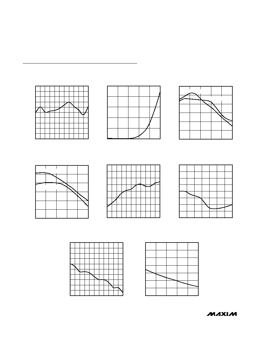
Typical Operating Characteristics
(V
DD
= +10V, V
SS
= -5V, V
L
= +5V, V
IN
= +5V, R
L
=
, C
L
= 0, AGND = DGND = 0, V
CH
= V
DD
, V
CL
= V
SS
, T
A
= +25∞C, unless
otherwise noted.)
0
0.4
0.2
1.0
0.8
0.6
1.2
1.4
1.8
1.6
2.0
-4
-2 -1
-3
0
1
2
3
4
5
6
7
DROOP RATE vs. INPUT VOLTAGE
MAX5168 TOC 01
INPUT VOLTAGE (V)
DROOP RATE (mV/s)
0
10
30
20
40
50
-40
10
-15
35
60
85
DROOP RATE vs. TEMPERATURE
MAX5168 TOC 02
TEMPERATURE (∞C)
DROOP RATE (mV/s)
0
-40
-20
-80
-60
-100
-120
0.1
10
1
100
1000
10,000
POWER-SUPPLY REJECTION RATIO
SAMPLE MODE
MAX5168 TOC 03
FREQUENCY (kHz)
PSRR (dB)
NEGATIVE SUPPLY (V
SS
)
POSITIVE SUPPLY (V
DD
)
0
-40
-20
-80
-60
-100
-120
0.1
10
1
100
1000
10,000
POWER-SUPPLY REJECTION RATIO
HOLD MODE
MAX5168 TOC 04
FREQUENCY (kHz)
PSRR (dB)
NEGATIVE SUPPLY (V
SS
)
POSITIVE SUPPLY (V
DD
)
0
-20
-140
-60
-40
-80
-100
-120
-160
-4
-2 -1
0
-3
1
2
5
4
6
3
7
HOLD STEP vs. INPUT VOLTAGE
MAX5168 TOC 05
INPUT VOLTAGE (V)
HOLD STEP (
µ
V)
80
90
85
100
95
115
110
105
120
-55
-15
-35
5
25
45
65
85
HOLD STEP vs. TEMPERATURE
MAX5168 TOC 06
TEMPERATURE (∞C)
HOLD STEP (
µ
V)
-5.0
-4.6
-4.8
-4.0
-4.2
-4.4
-3.8
-3.6
-3.2
-3.4
-3.0
-4
-2 -1
-3
0
1
2
3
4
5
6
7
OFFSET VOLTAGE vs. INPUT VOLTAGE
MAX5168 TOC 07
INPUT VOLTAGE (V)
OFFSET VOLTAGE (mV)
-7
-5
-6
-3
-4
-1
-2
0
-40
10
-15
35
60
85
OFFSET VOLTAGE vs. TEMPERATURE
MAX5168 TOC 08
TEMPERATURE (∞C)
OFFSET VOLTAGE (mV)

MAX5168
32-Channel Sample/Hold Amplifier
with a Single Multiplexed Input
_______________________________________________________________________________________
5
NAME
FUNCTION
1
ADDR2
Bit 2 of the Address Decoder
2
ADDR3
Bit 3 of the Address Decoder
PIN
3
ADDR4
Bit 4 of the Address Decoder
4
SELECT
Enables the S/H pin. The polarity of SELECT is determined by the state of the CONFIG pin. If CONFIG
is low, then SELECT is active-high. If CONFIG is high, then SELECT is active-low. When SELECT is not
in its active state, all 32 channels are in hold mode independent of the S/H pin.
8
DGND
Digital GND
7
V
L
+5V Logic Supply
6
CONFIG
Sets the polarity of the SELECT pin.
5
S/H
Puts the selected channel into sample mode when low. Places all channels into hold mode when high.
12, 13
N.C.
No connection. Not internally connected.
11
IN
Input Pin
10
AGND
Analog GND
9
V
SS
-5V Analog Supply
Pin Description
47
ADDR0
Bit 0 of the Address Decoder
31≠46
OUT16≠OUT31
Outputs 16≠31 Pins
30
V
DD
+10V Analog Supply
14≠29
OUT0≠OUT15
Outputs 0≠15 Pins
48
ADDR1
Bit 1 of the Address Decoder