 | –≠–ª–µ–∫—Ç—Ä–æ–Ω–Ω—ã–π –∫–æ–º–ø–æ–Ω–µ–Ω—Ç: MAX5150 | –°–∫–∞—á–∞—Ç—å:  PDF PDF  ZIP ZIP |
_______________General Description
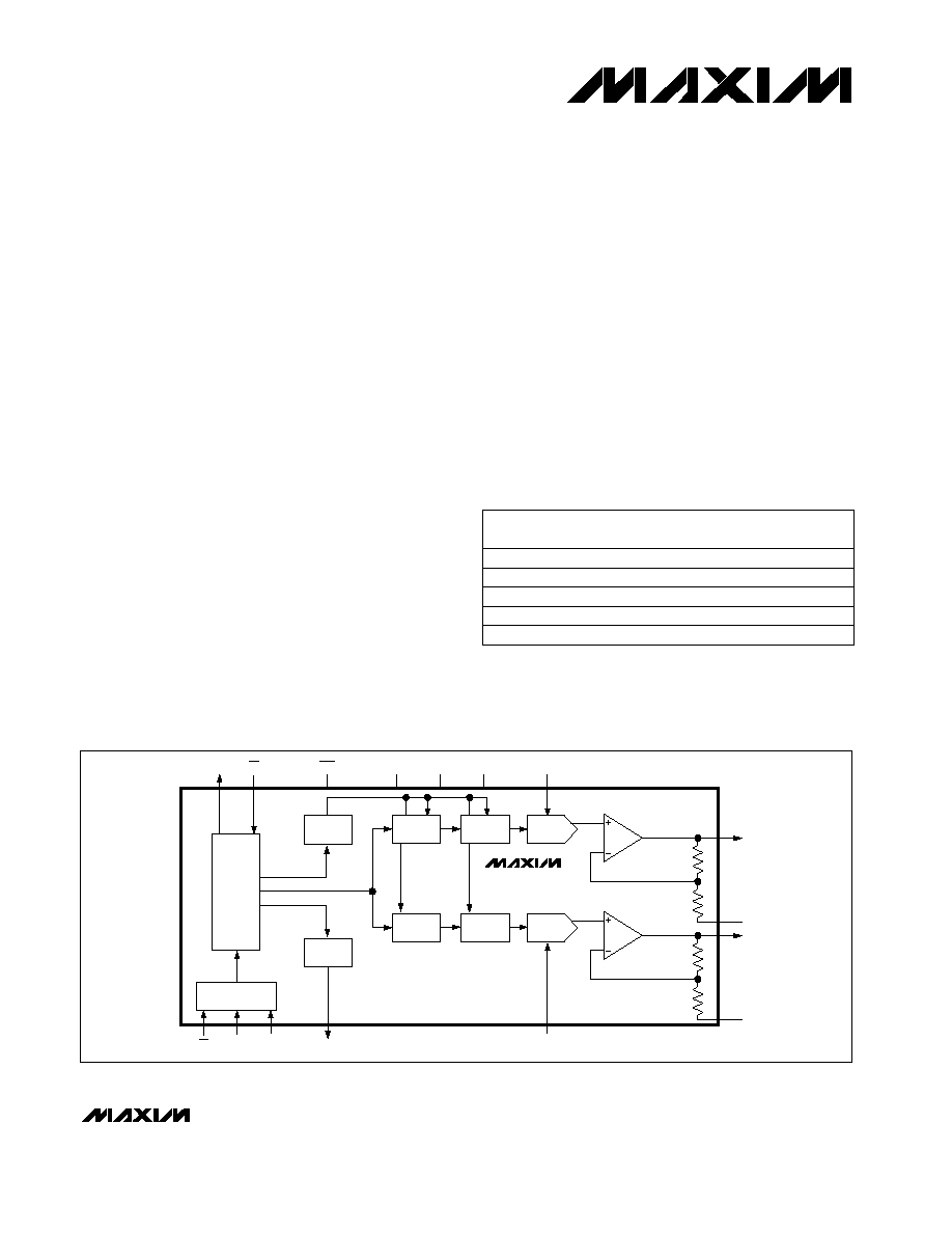
The MAX5150/MAX5151 low-power, serial, voltage-out-
put, dual 13-bit digital-to-analog converters (DACs)
consume only 500µA from a single +5V (MAX5150) or
+3V (MAX5151) supply. These devices feature Rail-to-
Rail
Æ
output swing and are available in a space-saving
16-pin QSOP package. To maximize the dynamic
range, the DAC output amplifiers are configured with an
internal gain of +2.
The 3-wire serial interface is SPITM/QSPITM and
MicrowireTM compatible. Each DAC has a double-
buffered input organized as an input register followed
by a DAC register, which allows the input and DAC reg-
isters to be updated independently or simultaneously
with a 16-bit serial word. Additional features include
programmable shutdown (2µA), hardware-shutdown
lockout, a separate reference voltage input for each
DAC that accepts AC and DC signals, and an active-
low clear input (CL) that resets all registers and DACs
to zero. These devices provide a programmable logic
pin for added functionality, and a serial-data output pin
for daisy-chaining.
________________________Applications
Industrial Process Control
Remote Industrial Controls
Digital Offset and Gain
Microprocessor-
Adjustment
Controlled Systems
Motion Control
Automatic Test
Equipment (ATE)
____________________________Features
o
13-Bit Dual DAC with Internal Gain of +2
o
Rail-to-Rail Output Swing
o
16µs Settling Time
o
Single-Supply Operation: +5V (MAX5150)
+3V (MAX5151)
o
Low Quiescent Current: 500µA (normal operation)
2µA (shutdown mode)
o
SPI/QSPI and Microwire Compatible
o
Available in Space-Saving 16-Pin QSOP Package
o
Power-On Reset Clears Registers and DACs
to Zero
o
Adjustable Output Offset
MAX5150/MAX5151
Low-Power, Dual, 13-Bit Voltage-Output DACs
with Serial Interface
________________________________________________________________
Maxim Integrated Products
1
19-1255; Rev 0; 8/97
______________Ordering Information
Rail-to-Rail is a registered trademark of Nippon Motorola Ltd.
SPI and QSPI are trademarks of Motorola, Inc.
Microwire is a trademark of National Semiconductor Corp.
For free samples & the latest literature: http://www.maxim-ic.com, or phone 1-800-998-8800
For small orders, phone 408-737-7600 ext. 3468.
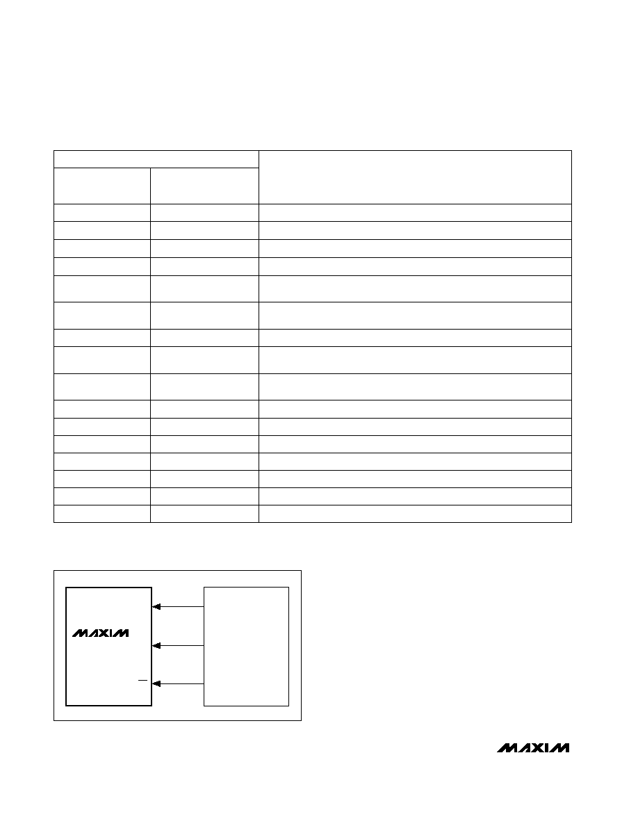
REFA
V
DD
AGND
DGND
PDL
CL
DOUT
16-BIT
SHIFT
REGISTER
SERIAL
CONTROL
INPUT
REG A
SCLK
UPO
REFB
DIN
CS
DAC A
DAC B
OUTB
R
R
FBB
OUTA
R
R
FBA
DAC
REG A
INPUT
REG B
LOGIC
OUTPUT
DECODE
CONTROL
DAC
REG B
MAX5150
MAX5151
_________________________________________________________Functional Diagram
Ordering Information continued at end of data sheet.
*
Dice are tested at T
A
= +25∞C, DC parameters only.
INL
(LSB)
PIN-PACKAGE
TEMP. RANGE
PART
±1
±1/2
±1
±1/2
16 QSOP
16 QSOP
16 Plastic DIP
16 Plastic DIP
0∞C to +70∞C
0∞C to +70∞C
0∞C to +70∞C
0∞C to +70∞C
MAX5150BCEE
MAX5150ACEE
MAX5150BCPE
MAX5150
ACPE
Pin Configuration appears at end of data sheet.
±1
Dice*
0∞C to +70∞C
MAX5150BC/D

MAX5150/MAX5151
Low-Power, Dual, 13-Bit Voltage-Output DACs
with Serial Interface
2
_______________________________________________________________________________________
ABSOLUTE MAXIMUM RATINGS
ELECTRICAL CHARACTERISTICS--MAX5150
(V
DD
= +5V ±10%, V
REFA
= V
REFB
= 2.048V, R
L
= 10k
, C
L
= 100pF, T
A
= T
MIN
to T
MAX
, unless otherwise noted. Typical values are
at T
A
= +25∞C (OS_ tied to AGND for a gain of +2).)
Stresses beyond those listed under "Absolute Maximum Ratings" may cause permanent damage to the device. These are stress ratings only, and functional
operation of the device at these or any other conditions beyond those indicated in the operational sections of the specifications is not implied. Exposure to
absolute maximum rating conditions for extended periods may affect device reliability.
V
DD
to AGND............................................................-0.3V to +6V
V
DD
to DGND ...........................................................-0.3V to +6V
AGND to DGND ..................................................................±0.3V
OSA, OSB to AGND........................(AGND - 4V) to (V
DD
+ 0.3V)
REF_, OUT_ to AGND.................................-0.3V to (V
DD
+ 0.3V)
Digital Inputs (SCLK, DIN, CS, CL, PDL)
to DGND ..............................................................-0.3V to +6V
Digital Outputs (DOUT, UPO)
to DGND ................................................-0.3V to (V
DD
+ 0.3V)
Maximum Current into Any Pin .........................................±20mA
Continuous Power Dissipation (T
A
= +70∞C)
Plastic DIP (derate 10.5mW/∞C above +70∞C) ...........842mW
QSOP (derate 8.30mW/∞C above +70∞C) ...................667mW
CERDIP (derate 10.00mW/∞C above +70∞C) ..............800mW
Operating Temperature Ranges
MAX515_ _C_ E .................................................0∞C to +70∞C
MAX515_ _E_ E ..............................................-40C∞ to +85∞C
MAX515_ _MJE.............................................-55∞C to +125∞C
(Note 1)
Input code = 0000 hex,
V
REF_
= (V
DD
- 1.4Vp-p) at 1kHz
Input code = 1FFF hex,
V
REF_
= 0.67Vp-p at 2.5V
DC
4.5V
V
DD
5.5V
Minimum with code 1555 hex
Normalized to 2.048V
Guaranteed monotonic
Code = 12
Normalized to 2.048V
dB
-82
Reference Feedthrough
kHz
300
Reference 3dB Bandwidth
k
14
20
R
REF
Reference Input Resistance
REF
Reference Input Range
V
0
V
DD
- 1.4
±1
LSB
±1/2
INL
Bits
13
Resolution
Integral Nonlinearity
PSRR
V
DD
Power-Supply
Rejection Ratio
µV/V
20
260
ppm/∞C
4
Gain-Error Tempco
LSB
±1
DNL
Differential Nonlinearity
mV
±6
Vos
Offset Error
ppm/∞C
4
TCVos
Offset Tempco
mV
-0.2
±3
Gain Error
MAX5150A
MAX5150B
CONDITIONS
UNITS
MIN
TYP
MAX
SYMBOL
PARAMETER
Input code = 1FFF hex,
V
REF_
= 1Vp-p at 1.25V
DC
, f = 25kHz
dB
75
SINAD
Signal-to-Noise plus
Distortion Ratio
CL, PDL, CS, DIN, SCLK
V
0.8
V
IL
Input Low Voltage
V
IN
= 0V to V
DD
µA
0.001
±1
I
IN
Input Leakage Current
pF
8
C
IN
Input Capacitance
mV
200
V
HYS
Input Hysteresis
CL, PDL, CS, DIN, SCLK
V
3.0
V
IH
Input High Voltage
REFERENCE INPUT
STATIC PERFORMANCE--ANALOG SECTION
MULTIPLYING-MODE PERFORMANCE
DIGITAL INPUTS
MAX5150/MAX5151
Low-Power, Dual, 13-Bit Voltage-Output DACs
with Serial Interface
_______________________________________________________________________________________
3
ELECTRICAL CHARACTERISTICS--MAX5150 (continued)
(V
DD
= +5V ±10%, V
REFA
= V
REFB
= 2.048V, R
L
= 10k
, C
L
= 100pF, T
A
= T
MIN
to T
MAX
, unless otherwise noted. Typical values are
at T
A
= +25∞C (OS_ tied to AGND for a gain of +2).)
CONDITIONS
Rail-to-rail (Note 2)
To 1/2LSB of full-scale, V
STEP
= 4V
I
SOURCE
= 2mA
UNITS
I
SINK
= 2mA
k
24
34
R
OS
OSA or OSB Input Resistance
V
0 to V
DD
Output Voltage Swing
µs
16
Output Settling Time
V/µs
0.75
SR
Voltage Output Slew Rate
V
OL
Output Low Voltage
V
0.13
0.4
MIN
TYP
MAX
SYMBOL
PARAMETER
V
OH
Output High Voltage
V
V
DD -
0.5
µs
25
Time Required to Exit Shutdown
CS = V
DD
, f
DIN
= 100kHz, V
SCLK
= 5Vp-p
nV-s
5
Digital Feedthrough
nV-s
5
Digital Crosstalk
V
4.5
5.5
V
DD
Positive Supply Voltage
(Note 3)
mA
0.5
0.65
I
DD
Power-Supply Current
(Note 3)
µA
2
10
I
DD (SHDN)
Power-Supply Current
in Shutdown
µA
0
±1
Reference Current in Shutdown
ns
100
t
CP
SCLK Clock Period
ns
40
t
CH
SCLK Pulse Width High
ns
40
t
CL
SCLK Pulse Width Low
ns
40
t
CSS
CS Fall to SCLK Rise
Setup Time
ns
0
t
CSH
SCLK Rise to CS Rise Hold Time
ns
40
t
DS
SDI Setup Time
ns
0
t
DH
SDI Hold Time
C
LOAD
= 200pF
ns
80
t
DO1
SCLK Rise to DOUT
Valid Propagation Delay
Note 1:
Accuracy is specified from code 12 to code 8191.
Note 2:
Accuracy is better than 1LSB for V
OUT
_ greater than 6mV and less than V
DD
- 50mV. Guaranteed by PSRR test at the end
points.
Note 3:
Digital inputs are set to either V
DD
or DGND, code = 0000 hex, R
L
=
.
C
LOAD
= 200pF
ns
80
t
DO2
SCLK Fall to DOUT
Valid Propagation Delay
ns
40
t
CS1
CS Rise to SCLK Rise Hold
ns
100
t
CSW
CS Pulse Width High
ns
10
t
CS0
SCLK Rise to CS Fall Delay
DYNAMIC PERFORMANCE
POWER SUPPLIES
DIGITAL OUTPUTS
TIMING CHARACTERISTICS
Resolution
MAX5150/MAX5151
Low-Power, Dual, 13-Bit Voltage-Output DACs
with Serial Interface
4
_______________________________________________________________________________________
ELECTRICAL CHARACTERISTICS--MAX5151
(V
DD
= +2.7V to +3.6V, V
REFA
= V
REFB
= 1.25V, R
L
= 10k
, C
L
= 100pF, T
A
= T
MIN
to T
MAX
, unless otherwise noted. Typical values
are at T
A
= +25∞C (OS_ pins tied to AGND for a gain of +2).)
nV-s
5
Digital Crosstalk
CS = V
DD
, f
DIN
= 100kHz, V
SCLK
= 3Vp-p
nV-s
5
Digital Feedthrough
µs
25
Time Required for Valid
Operation after Shutdown
Input code = 1FFF hex,
V
REF_
= 1Vp-p at 1V
DC
, f = 15kHz
dB
73
SINAD
Signal-to-Noise plus
Distortion Ratio
(Note 4)
Input code = 0000 hex,
V
REF_
= (V
DD
- 1.4)Vp-p at 1kHz
Input code = 1FFF hex,
V
REF_
= 0.67Vp-p at 0.75V
DC
CL, PDL, CS, DIN, SCLK
2.7V
V
DD
3.6V
Minimum with code 1555 hex
Normalized to 1.25V
Guaranteed monotonic
Code = 20
Normalized to 1.25V
V
0.8
VIL
Input Low Voltage
V
IN
= 0V to V
DD
µA
0
±1
IIN
Input Leakage Current
pF
8
C
IN
Input Capacitance
mV
200
VHYS
Input Hysteresis
CL, PDL, CS, DIN, SCLK
V
dB
-82
Reference Feedthrough
kHz
300
Reference 3dB Bandwidth
2.2
VIH
Input High Voltage
k
14
20
R
REF
Reference Input Resistance
±2
MAX5151A
MAX5151B
LSB
±1
INL
Bits
13
Integral Nonlinearity
PSRR
V
DD
Power-Supply
Rejection Ratio
µV/V
40
320
ppm/∞C
6.5
Gain-Error Tempco
LSB
±1
DNL
Differential Nonlinearity
mV
±6
Vos
Offset Error
ppm/∞C
6.5
TCVos
Offset Tempco
mV
-0.2
±5
Gain Error
Rail-to-rail (Note 5)
I
SOURCE
= 2mA
k
24
34
R
OS
OSA or OSB Input Resistance
V
0 to V
DD
Output Voltage Swing
V
V
DD
- 0.5
VOH
Output High Voltage
CONDITIONS
UNITS
MIN
TYP
MAX
SYMBOL
PARAMETER
REF
Reference Input Range
V
0
V
DD
- 1.4
DIGITAL OUTPUTS
I
SINK
= 2mA
V
0.13
0.4
VOL
Output Low Voltage
To 1/2LSB of full-scale, V
STEP
= 2.5V
µs
16
Output Settling Time
V/µs
0.75
SR
Voltage Output Slew Rate
REFERENCE INPUT (VREF)
MULTIPLYING-MODE PERFORMANCE
DIGITAL INPUTS
STATIC PERFORMANCE--ANALOG
DYNAMIC PERFORMANCE

MAX5150/MAX5151
Low-Power, Dual, 13-Bit Voltage-Output DACs
with Serial Interface
_______________________________________________________________________________________
5
Note 4:
Accuracy is specified from code 20 to code 8191.
Note 5:
Accuracy is better than 1LSB for V
OUT
greater than 6mV and less than V
DD
- 80mV. Guaranteed by PSRR test at the end
points.
Note 6:
Digital inputs are set to either V
DD
or DGND, code = 0000 hex, R
L
=
.
ELECTRICAL CHARACTERISTICS--MAX5151 (continued)
(V
DD
= +2.7V to +3.6V, V
REFA
= V
REFB
= 1.25V, R
L
= 10k
, C
L
= 100pF, T
A
= T
MIN
to T
MAX
, unless otherwise noted. Typical values
are at T
A
= +25∞C (OS_ pins tied to AGND for a gain of +2).)
C
LOAD
= 200pF
ns
120
t
DO2
SCLK Fall to DOUT Valid
Propagation Delay
ns
100
t
CSW
CS Pulse Width High
ns
40
t
CS1
CS Rise to SCLK Rise Hold
ns
10
t
CS0
SCLK Rise to CS Fall Delay
CONDITIONS
UNITS
(Note 6)
mA
0.45
0.6
I
DD
Power-Supply Current
(Note 6)
µA
1
8
I
DD (SHDN)
Power-Supply Current
in Shutdown
µA
MIN
TYP
MAX
0
±1
Reference Current in Shutdown
ns
100
SYMBOL
PARAMETER
t
CP
SCLK Clock Period
ns
40
t
CH
SCLK Pulse Width High
ns
40
t
CL
SCLK Pulse Width Low
ns
40
t
CSS
CS Fall to SCLK Rise
Setup Time
ns
0
t
CSH
SCLK Rise to CS Rise Hold Time
ns
50
t
DS
SDI Setup Time
ns
0
t
DH
SDI Hold Time
C
LOAD
= 200pF
ns
120
t
DO1
SCLK Rise to DOUT Valid
Propagation Delay
V
2.7
3.6
V
DD
Positive Supply Voltage
POWER SUPPLIES
TIMING CHARACTERISTICS

MAX5150/MAX5151
Low-Power, Dual, 13-Bit Voltage-Output DACs
with Serial Interface
6
_______________________________________________________________________________________
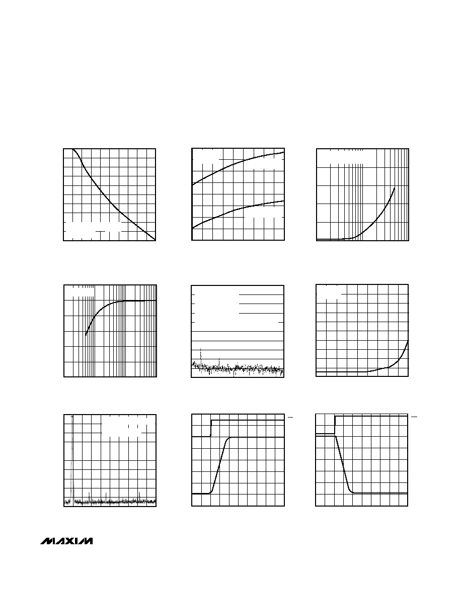
__________________________________________Typical Operating Characteristics
(V
DD
= +5V, R
L
= 10k
, C
L
= 100pF, OS_ pins tied to AGND, unless otherwise noted.)
-20
-16
-18
-12
-14
-8
-10
-6
-2
-4
0
1
370
740
1110
1480
1850
REFERENCE VOLTAGE INPUT
FREQUENCY RESPONSE
MAX5150/5151-01
FREQUENCY (kHz)
RELATIVE OUTPUT (dB)
V
REF
= 0.67Vp-p @ 2.5V
DC
CODE = 1FFF (HEX)
400
450
550
500
650
600
700
-55
5
-15
-35
45
25
65
105
85
125
SUPPLY CURRENT vs. TEMPERATURE
MAX5150/5151 toc05
TEMPERATURE (∞C)
SUPPLY CURRENT (
µ
A)
V
REF
= 2.048V
R
L
=
CODE = 1FFF (HEX)
CODE = 0000 (HEX)
-30
-80
1
10
100
TOTAL HARMONIC DISTORTION
PLUS NOISE vs. FREQUENCY
-70
MAX5150/5151 toc06
FREQUENCY (kHz)
THD + NOISE (dB)
-60
-50
-40
V
REF
= 1Vp-p @ 2.5V
DC
CODE = 1FFF (HEX)
0
0.1
1
10
100
FULL-SCALE ERROR vs. LOAD
-2.5
-2.0
-3.0
-1.5
-1.0
-0.5
0.5
1.0
MAX5150/5151 toc08
R
L
(k
)
FULL-SCALE ERROR (LSB)
V
REF
= 2.048V
-100
-80
-90
-60
-70
-40
-50
0.5
1.6
2.7
3.8
4.9
6.0
-30
-10
-20
0
OUTPUT FFT PLOT
MAX5150/5151 toc12
V
REF
= 2.45Vp-p @ 1.225V
DC
f = 1kHz
CODE = 1FFF (HEX)
NOTE: RELATIVE TO FULL-SCALE
FREQUENCY (kHz)
RELATIVE OUTPUT (dB)
-150
-130
-140
-110
-120
-90
-100
-80
-60
-70
-50
0.5
1.5 2.0 2.5
1.0
3.0 3.5 4.0
5.0
4.5
5.5
REFERENCE FEEDTHROUGH AT 1kHz
MAX5150/5151 toc10
FREQUENCY (kHz)
RELATIVE OUTPUT (dB)
V
REF
= 3Vp-p @ 1.5V
DC
f = 1kHz
CODE = 0000 (HEX)
NOTE: RELATIVE TO FULL-SCALE OUTPUT
0
1
2
3
4
5
6
-55
5
25
-15
-35
45
65
85 105 125
SHUTDOWN CURRENT
vs. TEMPERATURE
MAX5150/5151 toc13
TEMPERATURE (∞C)
SHUTDOWN CURRENT (
µ
A)
V
REF
= 1V
DYNAMIC RESPONSE RISE TIME
MAX5150/5151 toc17
2
µ
s/div
OUT_
1V/div
5V/div
CS
V
REF
= 2.048V
2
µ
s/div
DYNAMIC RESPONSE FALL TIME
MAX5150/5151 toc18
V
REF
= 2.048V
OUT_
1V/div
5V/div
CS
MAX5150
MAX5150/MAX5151
Low-Power, Dual, 13-Bit Voltage-Output DACs
with Serial Interface
_______________________________________________________________________________________
7
_____________________________Typical Operating Characteristics (continued)
(V
DD
= +3V, R
L
= 10k
, C
L
= 100pF, OS_pins tied to AGND, unless otherwise noted.)
-20
-16
-18
-12
-14
-8
-10
-6
-2
-4
0
1
320
640
960
1280
1600
REFERENCE VOLTAGE INPUT
FREQUENCY RESPONSE
MAX5150/5151 toc15
FREQUENCY (kHz)
RELATIVE OUTPUT (dB)
V
REF
= 0.67Vp-p @ 0.75V
DC
CODE = 1FFF
400
440
420
500
480
460
540
520
560
-55
5
25
-35 -15
45
65
85 105 125
SUPPLY CURRENT vs. TEMPERATURE
MAX5150/5151 toc04
TEMPERATURE (∞C)
SUPPLY CURRENT (
µ
A)
V
REF
= 1V
R
L
=
CODE = 1FFF (HEX)
CODE = 0000 (HEX)
-30
-80
1
10
100
TOTAL HARMONIC DISTORTION
PLUS NOISE vs. FREQUENCY
-70
MAX5150/5151 toc07
FREQUENCY (kHz)
THD + NOISE (dB)
-60
-50
-40
V
REF
= 1Vp-p @ 1V
DC
CODE = 1FFF (HEX)
0.5
-2.5
0.1
1
10
100
FULL-SCALE ERROR vs. LOAD
-1.0
-1.5
-2.0
-0.5
0
MAX5150/5151 toc09
R
L
(k
)
FULL-SCALE ERROR (LSB)
V
REF
= 1.25V
-100
-80
-90
-60
-70
-40
-50
-30
-10
-20
0
0.5
2.7
3.8
4.9
1.6
6.0
OUTPUT FFT PLOT
MAX5150/5151
FREQUENCY (kHz)
RELATIVE OUTPUT (dB)
V
REF
= 1.4Vp-p @ 0.75V
DC
f = 1kHz
CODE = 1FFF (HEX)
-150
-130
-140
-110
-120
-90
-100
-80
-60
-70
-50
0.5
1.5 2.0 2.5
1.0
3.0 3.5 4.0
5.0
4.5
5.5
REFERENCE FEEDTHROUGH AT 1kHz
MAX5150/5151 toc11
FREQUENCY (kHz)
RELATIVE OUTPUT (dB)
V
REF
= 2Vp-p @ 1V
DC
f = 1kHz
CODE = 0000 (HEX)
NOTE: RELATIVE TO FULL-SCALE OUTPUT
1.2
1.0
1.6
1.4
2.0
1.8
2.2
2.4
2.8
2.6
3.0
-55
-15
5
25
-35
45
65
85 105 125
SHUTDOWN CURRENT
vs. TEMPERATURE
MAX5150/5151 toc14
TEMPERATURE (∞C)
SHUTDOWN CURRENT (
µ
A)
V
REF
= 1V
R
L
=
DYNAMIC RESPONSE FALL TIME
MAX5150/5151 toc24
V
REF
= 1.25V
2
µ
s/div
OUT_
500mV/div
CS
2V/div
DYNAMIC RESPONSE RISE TIME
MAX5150/5151 toc20
2
µ
s/div
V
REF
=
1.25V
OUT_
500mV/div
2V/div
CS
MAX5151

MAX5150/MAX5151
Low-Power, Dual, 13-Bit Voltage-Output DACs
with Serial Interface
8
_______________________________________________________________________________________
_____________________________Typical Operating Characteristics (continued)
(V
DD
= +5V (MAX5150), V
DD
= +3V (MAX5151), R
L
= 10k
, C
L
= 100pF, OS_ pins tied to AGND, unless otherwise noted.)
0.40
0.45
0.50
0.55
0.60
0.65
2.0
2.5
3.0
3.5
4.0
4.5
5.0
5.5
6.0
SUPPLY CURRENT
vs. SUPPLY VOLTAGE
MAX5150/5151 TOC02
SUPPLY VOLTAGE (V)
SUPPLY CURRENT (mA)
R
L
=
MAX5150
MAX5151
CODE = 1FFF HEX
CODE = 0000 HEX
OUTB
200
µ
V/div
AC COUPLED
OUTA
5V/div
MAX5150
ANALOG CROSSTALK
MAX5150/5151 toc22
V
REF
= 2.048V, GAIN = +2, CODE = 1FFF HEX
250
µ
s/div
MAX5150
DIGITAL FEEDTHROUGH
MAX5150/5151 toc23
OUTA
500
µ
V/div
AC COUPLED
SCLK
5V/div
2.5
µ
s/div
5
µ
s/div
MAX5150
MAJOR-CARRY TRANSITION
MAX5150/5151 toc19
TRANSITION FROM 1000 HEX TO 0FFF HEX
OUT_
50mV/div
AC COUPLED
2V/div
CS
MAX5150/MAX5151

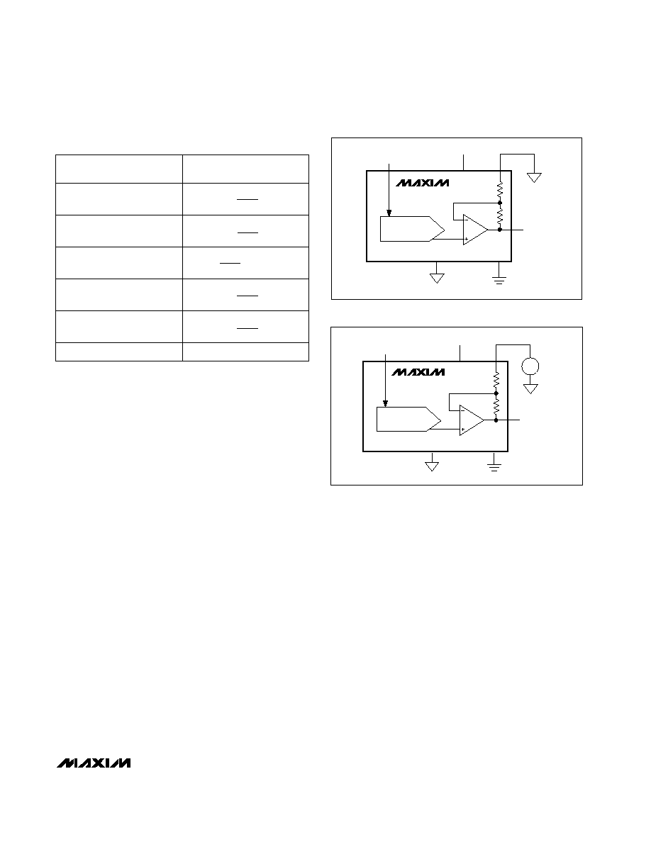
_______________Detailed Description
The MAX5150/MAX5151 dual, 13-bit, voltage-output
DACs are easily configured with a 3-wire serial inter-
face. These devices include a 16-bit data-in/data-out
shift register, and each DAC has a double-buffered
input composed of an input register and a DAC register
(see
Functional Diagram). In addition, trimmed internal
resistors produce an internal gain of +2 that maximizes
output voltage swing. The amplifier's offset-adjust pin
allows for a DC shift in the DAC's output.
Both DACs use an inverted R-2R ladder network that
produces a weighted voltage proportional to the input
voltage value. Each DAC has its own reference input to
facilitate independent full-scale values. Figure 1
depicts a simplified circuit diagram of one of the two
DACs.
Reference Inputs
The reference inputs accept both AC and DC values
with a voltage range extending from 0V to (V
DD
- 1.4V).
Determine the output voltage using the following equa-
tion (OS_ = AGND):
V
OUT
= (V
REF
x NB / 8192) x 2
where NB is the numeric value of the DAC's binary
input code (0 to 8191) and V
REF
is the reference volt-
age.
The reference input impedance ranges from 14k
(1555 hex) to several giga ohms (with an input code of
0000 hex). The reference input capacitance is code
dependent and typically ranges from 15pF with an
input code of all zeros to 50pF with an input code of all
ones.
Output Amplifier
The output amplifiers on the MAX5150/MAX5151 have
internal resistors that provide for a gain of +2 when OS_
is connected to AGND. These resistors are trimmed to
minimize gain error. The output amplifiers have a typi-
cal slew rate of 0.75V/µs and settle to 1/2LSB within
16µs, with a load of 10k
in parallel with 100pF. Loads
less than 2k
degrade performance.
The OS_ pin can be used to produce an adjustable off-
set voltage at the output. For instance, to achieve a 1V
offset, apply -1V to the OS_ pin to produce an output
range from 1V to (1V + V
REF
x 2). Note that the DAC's
output range is still limited by the maximum output volt-
age specification.
Power-Down Mode
The MAX5150/MAX5151 feature a software-program-
mable shutdown mode that reduces the typical supply
current to 2µA. The two DACs can be shutdown inde-
pendently, or simultaneously using the appropriate pro-
gramming command. Enter shutdown mode by writing
the appropriate input-control word (Table 1). In shut-
down mode, the reference inputs
and amplifier out-
MAX5150/MAX5151
Low-Power, Dual, 13-Bit Voltage-Output DACs
with Serial Interface
_______________________________________________________________________________________
9
Digital Ground
DGND
9
Serial-Data Output
DOUT
10
User-Programmable Output
UPO
11
Power-Down Lockout. The device can-
not be powered down when PDL is low.
PDL
12
Reference for DAC B
REFB
13
Clears all DACs and registers
(resets to 0).
CL
5
Chip-Select Input
CS
6
Serial-Data Input
DIN
7
Serial-Register Clock Input
SCLK
8
Reference for DAC A
REFA
4
DAC A Offset Adjustment
OSA
3
PIN
DAC A Output Voltage
OUTA
2
Analog Ground
AGND
1
FUNCTION
NAME
14
OSB
DAC B Offset Adjustment
15
OUTB
DAC B Output Voltage
16
V
DD
Positive Power Supply
OUT_
OS_
R
R
SHOWN FOR ALL 1s ON DAC
D0
D10
D11
D12
2R
2R
2R
2R
2R
R
R
R
REF_
AGND
Figure 1. Simplified DAC Circuit Diagram
_____________________Pin Description
MSB
LSB
MAX5150/MAX5151
puts become high impedance, and the serial inter-
face
remains active. Data in the input registers is
saved, allowing the MAX5150/MAX5151 to recall the
output state prior to entering shutdown when returning
to normal mode. Exit shutdown by recalling the previ-
ous condition or by updating the DAC with new infor-
mation. When returning to normal operation (exiting
shutdown), wait 20µs for output stabilization.
Serial Interface
The MAX5150/MAX5151 3-wire serial interface is com-
patible with both Microwire (Figure 2) and SPI/QSPI
(Figure 3) serial-interface standards. The 16-bit serial
input word consists of an address bit, two control bits,
and 13 bits of data (MSB to LSB) as shown in Figure 4.
Low-Power, Dual, 13-Bit Voltage-Output DACs
with Serial Interface
10
______________________________________________________________________________________
16-BIT SERIAL WORD
FUNCTION
A0
C1
C0
D12.......................D0
(MSB) (LSB)
0 0 1
13-bit DAC data
Load input register A; DAC registers are unchanged.
0 1 1
13-bit DAC data
Load all DAC registers from the shift register
(start up both DACs with new data.).
1 1 0
13-bit DAC data
Load input register B; all DAC registers are updated.
0 1 0
13-bit DAC data
Load input register A; all DAC registers are updated.
1 0 1
13-bit DAC data
Load input register B; DAC registers are unchanged.
0 0 0
1 1 0 x xxxxxxxxx
Shut down DAC A (provided PDL = 1).
0 0 0
1 0 1 x xxxxxxxxx
Update DAC register B from input register B
(start up DAC B with data previously stored in input register B).
0 0 0
0 0 1 x xxxxxxxxx
Update DAC register A from input register A
(start up DAC A with data previously stored in input register A).
1 1 1
xxxxxxxxxxxxx
Shut down both DACs (provided PDL = 1).
1 0 0
xxxxxxxxxxxxx
Update both DAC registers from their respective input registers
(start up both DACs with data previously stored in the input registers).
0 0 0
1 1 1 x xxxxxxxxx
Shut down DAC B (provided PDL = 1).
0 0 0
0 1 0 x xxxxxxxxx
UPO goes low (default).
0 0 0
0 1 1 x xxxxxxxxx
UPO goes high.
0 0 0
1 0 0 1 xxxxxxxxx
Mode 1, DOUT clocked out on SCLK's rising edge.
0 0 0
1 0 0 0 xxxxxxxxx
Mode 0, DOUT clocked out on SCLK's falling edge (default).
0 0 0
0 0 0 x xxxxxxxxx
No operation (NOP).
Table 1. Serial-Interface Programming Commands
x = Don't care
Note: When A0, C1, and C0 = 0, then D12, D11, D10, and D9 become control bits.
SCLK
DIN
CS
SK
SO
I/O
MAX5150
MAX5151
MICROWIRE
PORT
Figure 2. Connections for Microwire

The address and control bits determine the MAX5150/
MAX5151's response, as outlined in Table 1.
The MAX5150/MAX5151's digital inputs are double
buffered, which allows any of the following: loading the
input register(s) without updating the DAC register(s),
updating the DAC register(s) from the input register(s),
or updating the input and DAC registers concurrently.
The address and control bits allow the DACs to act
independently.
The 16-bit data can be sent as two 8-bit packets (SPI,
Microwire), with CS low during this period. The address
and control bits determine which register will be updat-
ed, and the state of the registers when exiting shut-
down. The 3-bit address/control determines the
following:
∑ registers to be updated
∑ clock edge on which data is to be clocked out via
the serial-data output (DOUT)
∑ state of the user-programmable logic output
∑ configuration of the device after shutdown.
The general timing diagram of Figure 5 illustrates how
data is acquired. Driving CS low enables the device to
receive data. Otherwise, the interface control circuitry is
disabled. With CS low, data at DIN is clocked into the
register on the rising edge of SCLK. As CS goes high,
data is latched into the input and/or DAC registers
depending on the address and control bits. The maxi-
mum clock frequency guaranteed for proper operation
is 10MHz. Figure 6 depicts a more detailed timing dia-
gram of the serial interface.
MAX5150/MAX5151
Low-Power, Dual, 13-Bit Voltage-Output DACs
with Serial Interface
DIN
SCLK
CS
MOSI
SCK
I/O
SPI/QSPI
PORT
SS
+5V
CPOL = 0, CPHA = 0
MAX5150
MAX5151
Figure 3. Connections for SPI/QSPI
Figure 5. Serial-Interface Timing Diagram
CS
SCLK
DIN
COMMAND
EXECUTED
9
8
16
1
C1
A0
D0
C0
D12 D11 D10
D9
D6
D5
D4
D3
D2
D1
D8
D7
______________________________________________________________________________________
11
MSB.......Data Bits.........LSB
D12.................................D0
13 Data Bits
16 Bits of Serial Data
Control Bits
C1, C0
Address Bits
MSB ..................................................................................LSB
A0
1 Address/2 Control Bits
Figure 4. Serial-Data Format

MAX5150/MAX5151
Low-Power, Dual, 13-Bit Voltage-Output DACs
with Serial Interface
12
______________________________________________________________________________________
SCLK
DIN
t
CSO
t
CSS
t
CL
t
CH
t
CP
t
CSW
t
CS1
t
CSH
t
DS
t
DH
CS
Figure 6. Detailed Serial-Interface Timing Diagram
TO OTHER
SERIAL DEVICES
MAX5150
MAX5151
DIN
SCLK
CS
MAX5150
MAX5151
MAX5150
MAX5151
DIN
DOUT
DOUT
DOUT
SCLK
CS
DIN
SCLK
CS
TO OTHER
SERIAL DEVICES
MAX5150
MAX5151
DIN
SCLK
CS
MAX5150
MAX5151
DIN
SCLK
CS
MAX5150
MAX5151
DIN
SCLK
CS
DIN
SCLK
CS1
CS2
CS3
Figure 7. Daisy Chaining MAX5150/MAX5151s
Figure 8. Multiple MAX5150/MAX5151s Sharing a Common DIN Line
Serial-Data Output
The serial-data output, DOUT, is the internal shift regis-
ter's output. DOUT allows for daisy chaining of devices
and data readback. The MAX5150/MAX5151 can be
programmed to shift data out of DOUT on SCLK's
falling edge (Mode 0) or on the rising edge (Mode 1).
Mode 0 provides a lag of 16 clock cycles, which main-
tains compatibility with SPI/QSPI and Microwire inter-
faces. In Mode 1, the output data lags 15.5 clock
cycles. On power-up, the device defaults to Mode 0.
User-Programmable Logic Output (UPO)
UPO allows an external device to be controlled through
the serial interface (Table 1), thereby reducing the
number of microcontroller I/O pins required.
Power-Down Lockout Input (
P
PD
DL
L
)
The power-down lockout pin (PDL) disables software
shutdown when low. When in shutdown, transitioning
PDL from high to low wakes up the part with the output
set to the state prior to shutdown. PDL can also be
used to asynchronously wake up the device.
Daisy Chaining Devices
Any number of MAX5150/MAX5151s can be daisy
chained by connecting the DOUT pin of one device to
the DIN pin of the following device in the chain (Figure 7).
Since the MAX5150/MAX5151's DOUT pin has an inter-
nal active pull-up, the DOUT sink/source capability
determines the time required to discharge/charge a
capacitive load. Refer to the serial-data-out V
OH
and
V
OL
specifications in the
Electrical Characteristics.
Figure 8 shows an alternate method of connecting sev-
eral MAX5150/MAX5151s. In this configuration, the
data bus is common to all devices; data is not shifted
through a daisy chain. More I/O lines are required in
this configuration because a dedicated chip-select
input (CS) is required for each IC.
__________Applications Information
Unipolar Output
Figure 9 shows the MAX5150/MAX5151 configured for
unipolar, rail-to-rail operation with a gain of +2. The
MAX5150 can produce a 0V to 4.096V output with
2.048V reference (Figure 9), while the MAX5151 can
produce a range of 0V to 2.5V with a 1.25V reference.
Table 2 lists the unipolar output codes. An offset to the
output can be achieved by connecting a voltage to
OS_, as shown in Figure 10. By applying V
OS
_ = -1V,
the output values will range between 1V and (1V +
V
REF
x 2).
MAX5150/MAX5151
Low-Power, Dual, 13-Bit Voltage-Output DACs
with Serial Interface
Table 2. Unipolar Code Table (Gain = +2)
MAX5150
MAX5151
DAC
GAIN = +2
REF_
OUT_
OS_
DGND
AGND
+5V/+3V
V
DD
R
R
Figure 9. Unipolar Output Circuit (Rail-to-Rail)
MAX5150
MAX5151
DAC _
AGND
DGND
REF_
OUT_
OS_
V
OS
+5V/+3V
V
DD
R
R
______________________________________________________________________________________
13
ANALOG OUTPUT
1 1 1 1 1
1 1 1 1
1 1 1 1
1 0 0 0 0
0 0 0 0
0 0 0 1
DAC CONTENTS
MSB
LSB
1 0 0 0 0
0 0 0 0
0 0 0 0
0 1 1 1 1
1 1 1 1
1 1 1 1
0 0 0 0 0
0 0 0 0
0 0 0 0
0V
0 0 0 0 0
0 0 0 0
0 0 0 1
+V
8191
8192
REF
x 2
+V
4097
8192
REF
x 2
+V
4096
8192
V
REF
REF
=
x 2
+V
4095
8192
REF
x 2
+V
1
8192
REF
x 2
Figure 10. Setting OS_ for Output Offset
MAX5150/MAX5151
Bipolar Output
The MAX5150/MAX5151 can be configured for a bipo-
lar output, as shown in Figure 11. The output voltage is
given by the equation (OS_ = AGND):
V
OUT
= V
REF
[((2 x NB) / 8192) - 1]
where NB represents the numeric value of the DAC's
binary input code. Table 3 shows digital codes and the
corresponding output voltage for Figure 11's circuit.
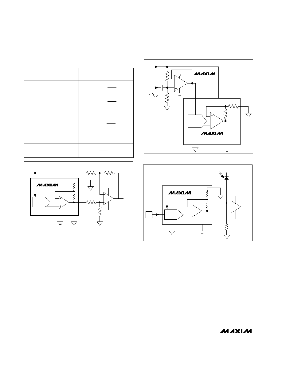
Using an AC Reference
In applications where the reference has an AC signal
component, the MAX5150/MAX5151 have multiplying
capabilities within the reference input voltage range
specifications. Figure 12 shows a technique for apply-
ing a sinusoidal input to REF_, where the AC signal is
offset before being applied to REF.
Harmonic Distortion and Noise
The total harmonic distortion plus noise (THD+N) is typ-
ically less than -78dB at full scale with a 1Vp-p input
swing at 5kHz. The typical -3dB frequency is 300kHz
for both devices, as shown in the
Typical Operating
Characteristics.
Digital Calibration and
Threshold Selection
Figure 13 shows the MAX5150/MAX5151 in a digital
calibration application. With a bright light value applied
to the photodiode (on), the DAC is digitally ramped until
it trips the comparator. The microprocessor stores this
"high" calibration value. Repeat the process with a
dim light (off) to obtain the dark current calibration.
Low-Power, Dual, 13-Bit Voltage-Output DACs
with Serial Interface
14
______________________________________________________________________________________
Table 3. Bipolar Code Table
ANALOG OUTPUT
1 1 1 1 1
1 1 1 1
1 1 1 1
1 0 0 0 0
0 0 0 0
0 0 0 1
DAC CONTENTS
MSB
LSB
1 0 0 0 0
0 0 0 0
0 0 0 0
0V
0 1 1 1 1
1 1 1 1
1 1 1 1
0 0 0 0 0
0 0 0 0
0 0 0 0
0 0 0 0 0
0 0 0 0
0 0 0 1
+V
4095
4096
REF
+V
1
4096
REF
-V
1
4096
REF
-V
4095
4096
REF
-V
4096
4096
- V
REF
REF
=
AGND
DGND
R
R
TOLERANCES: 10k
± 0.1%
MAX5150
MAX5151
DAC _
REF_
OS_
OUT_
10k
10k
10k
10k
V-
V+
V
DD
V
OUT
+5V/+3V
Figure 11. Bipolar Output Circuit
DAC_
OUT
MAX5150
MAX5151
10k
26k
OS_
REF
R
R
V
DD
GND
AGND
+5V/
+3V
AC
REFERENCE
INPUT
500mVp-p
MAX495
+5V/+3V
Figure 12. AC Reference Input Circuit
AGND
DIN
µ
P
DGND
MAX5150
MAX5151
DAC _
REF_
OS_
OUT_
R
R
V-
V+
PHOTODIODE
V+
V
DD
V
OUT
R
PULLDOWN
+5V/+3V
Figure 13. Digital Calibration

The microprocessor then programs the DAC to set an
output voltage at the midpoint of the two calibrated val-
ues. Applications include tachometers, motion sensing,
automatic readers, and liquid clarity analysis.
Digital Control of Gain and Offset
The two DACs can be used to control the offset and
gain for curve-fitting nonlinear functions, such as trans-
ducer linearization or analog compression/expansion
applications. The input signal is used as the reference
for the gain-adjust DAC, whose output is summed with
the output from the offset-adjust DAC. The relative
weight of each DAC output is adjusted by R1, R2, R3,
and R4 (Figure 14).
Power-Supply Considerations
On power-up, the input and DAC registers clear (set to
zero code). For rated performance, V
REF_
should be at
least 1.4V below V
DD
. Bypass the power supply with a
4.7µF capacitor in parallel with a 0.1µF capacitor to
AGND. Minimize lead lengths to reduce lead induc-
tance.
Grounding and Layout Considerations
Digital and AC transient signals on AGND can create
noise at the output. Connect AGND to the highest quali-
ty ground available. Use proper grounding techniques,
such as a multilayer board with a low-inductance
ground plane. Carefully lay out the traces between
channels to reduce AC cross-coupling and crosstalk.
Wire-wrapped boards and sockets are not recommend-
ed. If noise becomes an issue, shielding may be
required.
MAX5150/MAX5151
Low-Power, Dual, 13-Bit Voltage-Output DACs
with Serial Interface
______________________________________________________________________________________
15
AGND
DGND
MAX5150
MAX5151
DACA
V
DD
REFA
V
IN
V
REF
CS
SCLK
DIN
REFB
R1
R3
R
R
R
R
R4
R2
OUTB
OSB
OUTA
OSA
V
OUT
DACB
INPUT
REG A
INPUT
REG B
DAC
REG A
DAC
REG B
≠ OFFSET
[ ]
V
OUT
=
=
GAIN
[ ]
2NA
8192
NA IS THE NUMERIC VALUE OF THE INPUT CODE FOR DACA.
NB IS THE NUMERIC VALUE OF THE INPUT CODE FOR DACB.
R2
R1+R2
R4
R3
2NB
8192
R4
R3
(
V
IN
)(
)(
1+
) (
V
REF
)( )
[ ] [ ]
SHIFT
REGISTER
Figure 14. Digital Control of Gain and Offset

Maxim cannot assume responsibility for use of any circuitry other than circuitry entirely embodied in a Maxim product. No circuit patent licenses are
implied. Maxim reserves the right to change the circuitry and specifications without notice at any time.
16
____________________Maxim Integrated Products, 120 San Gabriel Drive, Sunnyvale, CA 94086 408-737-7600
© 1997 Maxim Integrated Products
Printed USA
is a registered trademark of Maxim Integrated Products.
MAX5150/MAX5151
Low-Power, Dual, 13-Bit Voltage-Output DACs
with Serial Interface
___________________Chip Information
TRANSISTOR COUNT: 3053
SUBSTRATE CONNECTED TO AGND
INL
(LSB)
PIN-PACKAGE
TEMP. RANGE
PART
±2
±2
±1
±2
±1
±1
±2
±1
±2
±1
±1
±1
±1/2
±1
±1/2
16 CERDIP**
-55∞C to +125∞C
MAX5151BMJE
16 QSOP
-40∞C to +85∞C
MAX5151BEEE
16 QSOP
-40∞C to +85∞C
MAX5151AEEE
16 Plastic DIP
-40∞C to +85∞C
MAX5151BEPE
16 Plastic DIP
-40∞C to +85∞C
MAX5151AEPE
Dice*
0∞C to +70∞C
MAX5151BC/D
16 QSOP
0∞C to +70∞C
MAX5151BCEE
16 QSOP
0∞C to +70∞C
MAX5151ACEE
16 Plastic DIP
0∞C to +70∞C
MAX5151BCPE
16 Plastic DIP
0∞C to +70∞C
MAX5151
ACPE
16 CERDIP**
-55∞C to +125∞C
MAX5150BMJE
16 QSOP
-40∞C to +85∞C
MAX5150BEEE
16 QSOP
-40∞C to +85∞C
MAX5150AEEE
16 Plastic DIP
-40∞C to +85∞C
MAX5150BEPE
16 Plastic DIP
-40∞C to +85∞C
MAX5150AEPE
_Ordering Information (continued)
*
Dice are tested at T
A
= +25∞C, DC parameters only.
**
Contact factory for availability.
16
15
14
13
12
11
10
9
1
2
3
4
5
6
7
8
AGND
V
DD
OUTB
OSB
REFB
PDL
UPO
DOUT
DGND
TOP VIEW
MAX5150
MAX5151
DIP/QSOP
OUTA
OSA
CS
REFA
CL
DIN
SCLK
__________________Pin Configuration
QSOP.EPS
________________________________________________________Package Information