 | –≠–ª–µ–∫—Ç—Ä–æ–Ω–Ω—ã–π –∫–æ–º–ø–æ–Ω–µ–Ω—Ç: MAX367 | –°–∫–∞—á–∞—Ç—å:  PDF PDF  ZIP ZIP |
_______________General Description
The MAX366 and MAX367 are multiple, two-terminal circuit
protectors. Placed in series with signal lines, each two-ter-
minal device guards sensitive circuit components against
voltages near and beyond the normal supply voltages.
These devices are used at interfaces where sensitive cir-
cuits are connected to the external world and could
encounter damaging voltages (up to 35V beyond the sup-
ply rails) during power-up, power-down, or fault conditions.
The MAX366 contains three independent protectors and
the MAX367 contains eight. They can protect analog sig-
nals using either unipolar (4.5V to 36V) or bipolar (±2.25V
to ±18V) power supplies. Each protector is symmetrical.
Input and output terminals may be freely interchanged.
These devices are voltage-sensitive MOSFET transistor
arrays that are normally on when power is applied and
normally open circuit when power is off. With ±10V sup-
plies, on-resistance is 100
max and leakage is less than
1nA at +25∞C.
When signal voltages exceed or are within approximately
1.5V of either power-supply voltage (including when
power is off), the two-terminal resistance increases dra-
matically, limiting fault current as well as output voltage to
sensitive circuits. The protected side of the switch main-
tains the correct polarity and clamps approximately 1.5V
below the supply rail. There are no "glitches" or polarity
reversals going into or coming out of a fault condition.
________________________Applications
Process Control Systems
Redundant/Backup Systems
Hot-Insertion Boards/Systems ATE Equipment
Data-Acquisition Systems
Sensitive Instruments
____________________________Features
o
±40V Overvoltage Protection
o
Open Signal Paths with Power Off
100
Signal Paths with Power On
o
1nA Max Path Leakage at +25∞C
o
44V Maximum Supply Voltage Rating
o
Automatic Protection; No Programming or
Controls
______________Ordering Information
MAX366/MAX367
Signal-Line Circuit Protectors
________________________________________________________________
Maxim Integrated Products
1
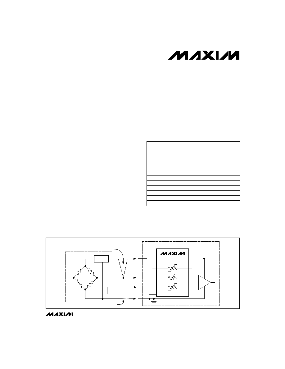
MAX366
OUT1
SENSITIVE
AMPLIFIER
1
FAULT!
FAULT!
IN1
(SHORT)
(OPEN)
REMOTE SENSOR
ELECTRONICS
7
+28V
+12V
OUT2
2
IN2
6
OUT3
3
IN3
5
V+
4
V-
PROTECTOR
+10V REG.
8
___________________________________________________Typical Operating Circuit
Call toll free 1-800-998-8800 for free samples or literature.
19-0326; Rev 0; 12/94
PART
MAX366
CPA
MAX366CSA
MAX366C/D
0∞C to +70∞C
0∞C to +70∞C
0∞C to +70∞C
TEMP. RANGE
PIN-PACKAGE
8 Plastic DIP
8 SO
Dice*
MAX366EPA
MAX366ESA
MAX366MJA
-55∞C to +125∞C
-40∞C to +85∞C
-40∞C to +85∞C
8 Plastic DIP
8 SO
8 CERDIP**
MAX367
CPN
MAX367CWN
MAX367C/D
0∞C to +70∞C
0∞C to +70∞C
0∞C to +70∞C
18 Plastic DIP
18 Wide SO
Dice*
MAX367EPN
MAX367EWN
MAX367MJN
-55∞C to +125∞C
-40∞C to +85∞C
-40∞C to +85∞C
18 Plastic DIP
18 Wide SO
18 CERDIP**
Pin Configurations appear at end of data sheet.
MAX367 available after January 1, 1995.
* Dice are tested at T
A
= +25∞C only.
* Contact factory for availability.

MAX366/MAX367
Signal-Line Circuit Protectors
2
_______________________________________________________________________________________
ABSOLUTE MAXIMUM RATINGS
ELECTRICAL CHARACTERISTICS
(V+ = +15V, V- = -15V, T
A
= T
MIN
to T
MAX
, unless otherwise noted.)
Stresses beyond those listed under "Absolute Maximum Ratings" may cause permanent damage to the device. These are stress ratings only, and functional
operation of the device at these or any other conditions beyond those indicated in the operational sections of the specifications is not implied. Exposure to
absolute maximum rating conditions for extended periods may affect device reliability.
Note 1:
Guaranteed, but not tested.
Note 2:
See
Typical Operating Characteristics curves for fault-free analog signal range at various supply voltages.
V+ to V-......................................................................-0.3V, +44V
IN_, OUT_ ..................................................(V- + 44V), (V+ - 44V)
Continuous Current into Any Terminal..............................±30mA
Peak Current into Any Terminal
(pulsed at 1ms, 10% duty cycle)...................................±70mA
Continuous Power Dissipation (T
A
= +70∞C)
8-Pin Plastic DIP (derate 9.09mW/∞C above +70∞C) ....727mW
8-Pin SO (derate 5.88mW/∞C above +70∞C).................471mW
8-Pin CERDIP (derate 8.00mW/∞C above +70∞C).........640mW
18-Pin Plastic DIP (derate 11.11mW/∞C above +70∞C) ...889mW
18-Pin Wide SO (derate 9.52mW/∞C above +70∞C) .....762mW
18-Pin CERDIP (derate 10.53mW/∞C above +70∞C).....842mW
Operating Temperature Ranges
MAX36_C_ _ ........................................................0∞C to +70∞C
MAX36_E_ _......................................................-40∞C to +85∞C
MAX36_M_ _ ...................................................-55∞C to +125∞C
Storage Temperature Range .............................-65∞C to +150∞C
Lead Temperature (soldering, 10sec) .............................+300∞C
V+ = V- = 0V, V
OUT
= 0V,
V
IN
= ±35V
V+ = 15V, V- = -15V (Note 2)
(Note 1)
V+ = 10V, V- = -10V, V
IN
= ±5V,
I
OUT
= 1mA
V
IN
= ±10V, I
OUT
= 1mA
V
IN
= V+ or V-,
100k
< R
OUT
< 1000M
(Note 1)
V+ = 15V, V- = -15V, V
IN
= ±10V,
I
OUT
= 1mA
V+ = 5V, V- = -5V, V
IN
= ±2V,
I
OUT
= 1mA
CONDITIONS
nA
-10
10
I
IN(OFF)
Signal-Path Leakage
(with Overvoltage)
10
R
(IN-OUT)
Signal-Path Resistance Match
7
400
R
(IN-OUT)
Analog-Signal-Path Resistance
V
-11
11
V
IN
, V
OUT
V
(V+ - 40)
(V- + 40)
V
IN
, V
OUT
Analog Signal Range
Fault-Free Analog Signal Range
140
350
150
125
62
100
V
(V- + 3)
(V+ - 1.5)
V
OUT
Analog-Signal Output
Range (Fault)
62
85
100
125
UNITS
MIN
TYP
MAX
SYMBOL
PARAMETER
+25∞C
All
All
+25∞C
M
C, E, M
C, E
+25∞C
All
+25∞C
C, E
+25∞C
M
C, E, M
TEMP.
RANGE
V+ = V- = 0V, V
IN
= ±35V,
V
OUT
= open circuit
nA
-1000
1000
I
IN(OFF)
Signal-Path Leakage
(Power Off)
-10
10
C, E, M
+25∞C
V
IN
= ±25V, V
OUT
= open circuit
nA
-1000
1000
I
IN(ON)
Signal-Path Leakage
(with Fault Condition)
-10
10
C, E, M
+25∞C
V
IN
= V
OUT
= ±10V
nA
-100
100
I
OUT(ON)
Signal-Path Leakage
(without Fault Condition)
-1
1
C, E, M
+25∞C
-1
1
+25∞C
R
(IN-OUT)
< 1000
(Note 2)
V
±2.25
±18
V+, V-
Power-Supply Range
(without Fault Condition)
+25∞C,
C, E, M
µA
-10
10
I+, I-
Power-Supply Current
C, E, M
V
0
±18
V+, V-
Power-Supply Range
+25∞C,
C, E, M
C, E, M
-1000
1000
POWER SUPPLY
MAX366/MAX367
Signal-Line Circuit Protectors
_______________________________________________________________________________________
3
-25
-35
15
25
35
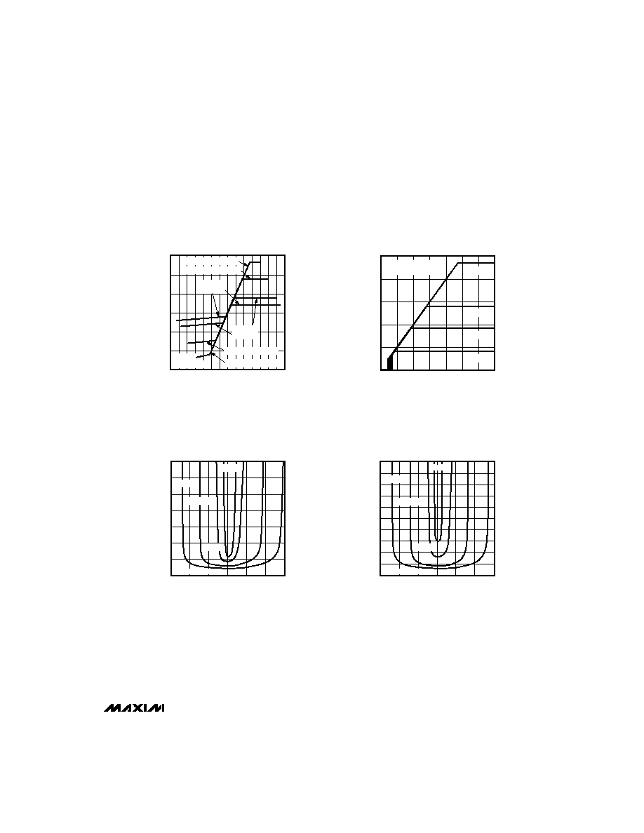
TRANSFER CHARACTERISTICS
(BIPOLAR SUPPLIES)
MAX366/7-02
INPUT VOLTAGE (V)
OUTPUT VOLTAGE (V),
INPUT & OUTPUT CURRENT (
µ
A)
0
-15
-5
5
-15
15
0
-10
-5
10
5
V+ = +3V,
V- = -3V
V+ = +5V,
V- = -5V
V+ = +15V, V- = -15V
V+ = +15V, V- = -15V
V+ = +10V, V- = -10V
V+ = +10V, V- = -10V
OUTPUT
LOAD = 1M
15
25
35
20
30
TRANSFER CHARACTERISTICS
(SINGLE SUPPLY)
MAX366/7-03
INPUT VOLTAGE (V)
V
IN
> (V+ - 35V)
OUTPUT VOLTAGE (V),
INPUT & OUTPUT CURRENT (
µ
A)
0
10
5
15
0
10
25
20
5
V+ = 25V
V+ = 15V
V+ = 10V
V+ = 5V
OUTPUT LOAD = 1M
V- = 0V
1E+01
1E+02
1E+03
1E+04
1E+05
1E+06
1E+07
1E+08
-15
15
PATH RESISTANCE vs. INPUT VOLTAGE
(BIPOLAR SUPPLIES)
MAX366/7-04
INPUT VOLTAGE (V)
PATH RESISTANCE (
)
0
-10
-5
10
5
V± = ±15V
Circuit of Fig. 6
V± = ±10V
V± = ±5V
V± = ±3V
500
0
-15
15
PATH RESISTANCE vs. INPUT VOLTAGE
(BIPOLAR SUPPLIES)
400
MAX366/7-05
INPUT VOLTAGE (V)
PATH RESISTANCE (
)
0
200
100
-10
-5
10
300
50
450
250
150
350
5
V± = ±15V
V± = ±10V
V± = ±5V
V± = ±3V
Circuit of Fig. 6
__________________________________________Typical Operating Characteristics
(V+ = +15V, V- = -15V, T
A
= +25∞C, unless otherwise noted.)
MAX366/MAX367
Signal-Line Circuit Protectors
4
_______________________________________________________________________________________
____________________________Typical Operating Characteristics (continued)
(V+ = +15V, V- = -15V, T
A
= +25∞C, unless otherwise noted.)
V+ = 5V, V- = -5V
CHAN 1: INPUT OVERVOLTAGE RAMP ±7V, 2V/div
CHAN 2: OUTPUT; OUTPUT LOAD = 1000
, 2V/div
OVERVOLTAGE RAMP
-12
10
MAX366 FREQUENCY RESPONSE
MAX366-TOC9
FREQUENCY (Hz)
LOSS (dB)
-10
-8
-6
-4
-2
0
1k
10k
100k
1M
10M 100M
100
SOURCE = 50
LOAD = 50
V+ = 5V
V- = -5V
100
PATH RESISTANCE vs. INPUT VOLTAGE
(SINGLE SUPPLY)
MAX366/7-06
INPUT VOLTAGE (V)
PATH RESISTANCE (
)
10
1
V+ = 35V
V+ = 25V
V+ = 15V
V+ = 10V
V+ = 5V
V- = 0V
10
100
1k
10k
100k
1M
10M
1G
100M
Circuit of Fig. 6
500
0
100
PATH RESISTANCE vs. INPUT VOLTAGE
(SINGLE SUPPLY)
400
MAX366/7-07
INPUT VOLTAGE (V)
PATH RESISTANCE (
)
200
100
10
1
300
50
450
250
150
350
V+ = 35V
V+ = 25V
V+ = 15V
V+ = 10V
V+ = 5V
V- = 0V
Circuit of Fig. 6

MAX366/MAX367
Signal-Line Circuit Protectors
_______________________________________________________________________________________
5
___________Background Information
When a voltage outside the supply range is applied to
most integrated circuits, there is a strong possibility they
will be damaged or "latch up" (that is, fail to operate prop-
erly even after the offending voltage is removed). If an
IC's input or output pin is supplied with a voltage when the
IC's power is off, and power is subsequently applied, the
device may act as an SCR and destroy itself and/or other
circuitry. Such "faults" are commonly encountered in
modular control systems where power and signals to inter-
connected modules may be interrupted and re-estab-
lished at random. They can happen during production
testing, maintenance, start-up, or a power "brownout."
The MAX366/MAX367 are designed to protect delicate
input and output circuitry from overvoltage faults up to
±40V (with or without power applied), in devices such as
op amps, analog-to-digital/digital-to-analog converters,
and voltage references. These circuit protectors automati-
cally limit signal voltages and currents to safe levels with-
out degrading normal signal performance, even in very
high-impedance circuits. They are powered by the power
supply of the protected circuit and inserted into the signal
lines. There are no control lines, programming pins, or
adjustments.
Unlike shunt diode networks, these devices are low-
impedance FETs that become high impedance during a
fault condition, so fault current and power dissipation are
extremely low. Equally important, leakage current during
normal and fault conditions is extremely low. In addition,
unlike most discrete networks, these parts protect circuits
both when power is off and during power transitions.
_______________Detailed Description
Internal Construction
Figure 1 shows the simplified internal construction of
each protector inside the MAX366/MAX367. Each circuit
consists of two N-channel FETs and one P-channel FET.
All the FETs are enhancement types; that is, the N chan-
nels must have approximately 1.3V of positive gate volt-
age in order to conduct, and the P channel must have
approximately 2V of negative gate voltage in order to
conduct.
During normal operation, V+ is connected to a positive
potential and V- is connected to a negative potential.
Since their gates are tied to V+, transistors Q1 and Q3
conduct as long as their sources are at least 1.3V below
V+ (the N-channel gate threshold.) Transistor Q2's gate
is tied to V-, so it conducts as long as its source is 2V or
more above V- (the P-channel gate threshold.)
______________________________________________________________Pin Description
PIN
MAX366
MAX367
FUNCTION
1, 2, 3
1, 2, 3
Signal Inputs 1, 2, 3
≠
4≠8
Signal Inputs 4≠8
4
9
Negative Supply Voltage Input
NAME*
IN1, IN2, IN3
8
18
Positive Supply Voltage Input
≠
10≠14
Signal Outputs 4≠8
IN4≠IN8
V-
V+
OUT8≠OUT4
5, 6, 7
15, 16, 17
Signal Outputs 1, 2, 3
OUT3, OUT2,
OUT1
* Inputs and outputs are names for convenience only; inputs and outputs are identical and interchangeable.
P
Q2
N
Q3
N
Q1
OUT
V+
V-
IN
Figure 1. Simplified Internal Structure