 | –≠–ª–µ–∫—Ç—Ä–æ–Ω–Ω—ã–π –∫–æ–º–ø–æ–Ω–µ–Ω—Ç: MAX3507 | –°–∫–∞—á–∞—Ç—å:  PDF PDF  ZIP ZIP |

General Description
The MAX3507 is a variable-gain power amplifier for use
in CATV upstream transmitters. The variable-gain fea-
ture has 55dB of dynamic range and is controlled by a
3-wire SPITM bus. The device is capable of generating
+64dBmV output (16QAM/QPSK) when driven with a
+34dBmV nominal input signal. The on-chip anti-alias
lowpass filter with 75MHz cutoff frequency saves sys-
tem design cost and space. The optional positive slope
generator provides system design flexibility.
The device operates from a single +5V supply and
draws 220mA nominal during transmit at max gain
(100% duty cycle). For burst-type transmissions, the
device is shut off between bursts to minimize noise and
save power while still maintaining a match at the output.
The device is optimized for high linearity with harmonic
levels below -55dBc.
The MAX3507 is available in a 28-pin QFN package
and operates over the extended industrial temperature
range (-40∞C to +85∞C).
Applications
Cable Modem Upstream Transmitter
Set-Top Box Upstream Transmitter
Telephony Over Cable
Features
o Built-In 5th-Order Elliptic Anti-Aliasing Filter
o 5MHz to 65MHz Operation
o 55dB Gain Control Range
o Optional Positive Slope Generator
o 55dB Spurious-Free Dynamic Range Over
Transmit Band
MAX3507
Upstream CATV Amplifier with
On-Chip Anti-Alias Filter
________________________________________________________________ Maxim Integrated Products
1
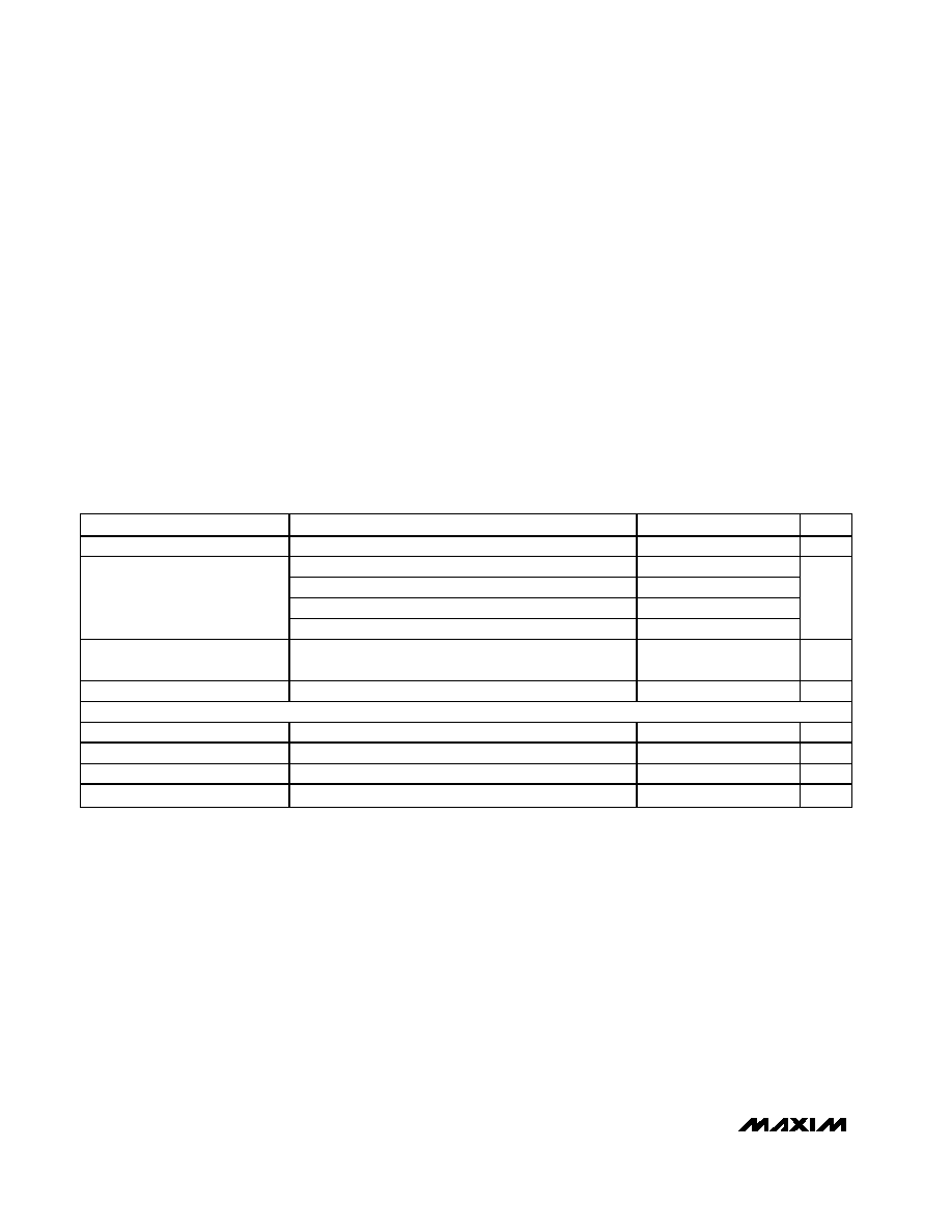
Ordering Information
28
26
25
24
23
22
27
16
17
15
20
21
18
19
10
8
12
13
9
11
14
5
4
3
2
1
7
6
V
CC
V
CC
BIASF
DC+
DC-
GND
IN+
IN-
V
CC
4:1
IMPEDANCE
RATIO
TXEN
N.C.
N.C.
CEXT
N.C.
OUT+
OUT-
DIGITAL
CONTROL
LINES
GND
SDA
SCLK
GND
N.C.
CS
SHDN
V
CC
OPTIONAL
EQUALIZER
5-POLE
ELLIPTIC
FILTER
V
CC
V
CC
EQ+
EQ-
GND
GND
N.C.
V
CC
V
CC
SERIAL DATA
GAIN
CONTROL
BIAS
CIRCUIT
MAX3507
Typical Operating Circuit
19-2092; Rev 0; 7/01
Pin Configuration appears at end of data sheet.
For pricing, delivery, and ordering information, please contact Maxim/Dallas Direct! at
1-888-629-4642, or visit Maxim's website at www.maxim-ic.com.
PART
TEMP. RANGE
PIN-PACKAGE
MAX3507EGI
-40∞C to +85∞C
28 QFN
SPI is a trademark of Motorola, Inc.
MAX3507
Upstream CATV Amplifier with
On-Chip Anti-Alias Filter
2
_______________________________________________________________________________________
ABSOLUTE MAXIMUM RATINGS
DC ELECTRICAL CHARACTERISTICS
(MAX3507 EV Kit, V
CC
= +4.75V to +5.25V, V
GND
= 0, V
TXEN
= V
SHDN
= V
CC
, D7 = 1, T
A
= -40∞C to +85∞C, unless otherwise speci-
fied. No input signal applied. A 4:1 (300
to 75) impedance ratio balun is connected to differential output ports and balun output is
terminated into a 75
load. Typical parameters are at V
CC
= +5.0V, T
A
= +25∞C.) (Note 1)
Stresses beyond those listed under "Absolute Maximum Ratings" may cause permanent damage to the device. These are stress ratings only, and functional
operation of the device at these or any other conditions beyond those indicated in the operational sections of the specifications is not implied. Exposure to
absolute maximum rating conditions for extended periods may affect device reliability.
V
CC
, OUT+, OUT- to GND.....................................-0.5V to +8.0V
Input Voltage Levels (all inputs),
C
EXT
to GND ...........................................-0.3V to (V
CC
+ 0.3V)
Continuous Input Voltage (IN+, IN-) ..................................2Vp-p
Continuous Current (OUT+, OUT-) ..................................120mA
Continuous Power Dissipation (T
A
= +70∞C)
28-Pin QFN (derate 20.8mW/∞C above +70∞C) ..............1.67W
Operating Temperature Range ...........................-40∞C to +85∞C
Junction Temperature ......................................................+150∞C
Storage Temperature Range .............................-65∞C to +125∞C
Bump Reflow Temperature ..............................................+300∞C
PARAMETER
CONDITIONS
MIN
TYP
MAX
UNITS
Supply Voltage
4.75
5.25
V
D7 = 1, gain code = 127 (max gain)
218
280
D7 = 1, gain code = 119 (gain of 28dB)
164
D7 = 1, gain code = 64 (gain of 0dB)
82
Supply Current Transmit Mode
D7 = 0, gain code = 94 (gain of 0dB)
74
mA
Supply Current Transmit Disable
Mode
V
TXEN
= V
EE
, V
SHDN
= V
CC
45
59
mA
Shutdown Supply Current
V
TXEN
= X, V
SHDN
= V
EE
1
µA
LOGIC INPUTS
Input HIGH Voltage Threshold
2.0
V
Input LOW Voltage Threshold
0.8
V
Input HIGH Current
100
µA
Input LOW Current
-100
µA

MAX3507
Upstream CATV Amplifier with
On-Chip Anti-Alias Filter
_______________________________________________________________________________________
3
AC ELECTRICAL CHARACTERISTICS
(MAX3507 EV Kit, V
CC
= +4.75V to +5.25V, V
GND
= 0, V
TXEN
= V
SHDN
= V
CC
, V
IN
= +34dBmV differential, T
A
= -40∞C to +85∞C,
unless otherwise specified. A 4:1 impedance ratio (300
to 75) balun is connected to differential output ports and balun output is
terminated into a 75
load. Typical parameters are at V
CC
= +5.0V, T
A
= +25∞C.) (Note 1)
PARAMETER
CONDITIONS
MIN
TYP
MAX
UNITS
D7 = 1, gain code = 125
29.6
31.1
32.6
D7 = 1, gain code = 119
26.8
28.3
29.8
D7 = 1, gain code = 104
19.5
20.9
22.3
D7 = 1, gain code = 84
9.7
10.9
12.1
D7 = 1, gain code = 64
-0.7
0.5
1.7
D7 = 0, gain code = 74
-10.5
-9.3
-8.1
D7 = 0, gain code = 54
-20.4
-19.1
-17.8
f
IN
= 5MHz,
T
A
= 0
∞C to +85∞C
(Note 2)
D7 = 0, gain code = 42
-27.2
-25.7
-24.2
Voltage Gain (A
V
)
f
IN
= 65MHz,
T
A
= 0∞C to +85
∞C
(Note 3)
D7 = 1, gain code = 127
29.0
dB
V
OU T
= 61d Bm V , f
IN
= 42M H z, eq ual i zer d i sab l ed ( N ote 3)
-1.1
-0.5
+0.2
Gain Flatness
V
OU T
= 61d Bm V , f
IN
= 65M H z, eq ual i zer d i sab l ed ( N ote 3)
-2.1
-0.7
+0.3
dB
f
IN
= 5MHz to 65MHz, A
V
= -26dB to +30dB
0.5
f
IN
= 5MHz to 65MHz, A
V
= -26dB to +30dB, any 2-bit
transition of D0, D1
0.7
1.0
1.3
Gain Step Size
f
IN
= 5MHz to 42MHz, D7 = 0, gain code = 109; D7 = 1,
gain code = 81, T
A
= 0∞C to +85∞C
0.6
1.0
1.4
dB
Transmit-Disable Mode Noise
Any BW = 160kHz from 5MHz to 65MHz, TXEN = V
EE
(Note 3)
-64
dBmV
Isolation in Transmit Disable
Mode
TXEN = V
EE
, f
IN
= 5MHz to 65MHz
70
dB
Transmit Mode Noise
Any BW = 160kHz from 5MHz to 65MHz, gain = -26dB to
+30dB (Note 3)
-54.5
dBc
Transmit Enable Transient
Duration
TXEN input rise/fall time < 0.1µs,
T
A
= +25
∞C (Notes 3, 4)
2
µs
Transmit Disable Transient
Duration
TXEN input rise/fall time < 0.1µs,
T
A
= +25
∞C (Notes 3, 4)
2
µs
D7 = 1, gain code = 119 (A
V
= >27dB), T
A
= +25∞C
100
Transmit Disable/Transmit
Enable Transient Step Size
D7 = 0, gain code = 94 (A
V
= 0), T
A
= +25∞C (Note 3)
1.5
5.2
mVp-p
Input Impedance
f
IN
= 5MHz to 65MHz, single ended (Note 3)
0.8
k
Output Return Loss
f
IN
= 5MHz to 42MHz in 75
system, D7 = 1,
gain code = 125 (A
V
= 30dB) (Note 5)
10
dB
Output Return Loss in Transmit
Disable Mode
f
IN
= 5M H z to 42M H z i n 75
system , TX E N = V
E E
( N ote 5)
10
dB
MAX3507
Upstream CATV Amplifier with
On-Chip Anti-Alias Filter
4
_______________________________________________________________________________________
AC ELECTRICAL CHARACTERISTICS (continued)
(MAX3507 EV Kit, V
CC
= +4.75V to +5.25V, V
GND
= 0, V
TXEN
= V
SHDN
= V
CC
, V
IN
= +34dBmV differential, T
A
= -40∞C to +85∞C,
unless otherwise specified. A 4:1 impedance ratio (300
to 75) balun is connected to differential output ports and balun output is
terminated into a 75
load. Typical parameters are at V
CC
= +5.0V, T
A
= +25∞C.) (Note 1)
TIMING CHARACTERISTICS
(MAX3507 EV Kit, V
CC
= +4.75V to +5.25V, V
GND
= 0, V
TXEN
= V
SHDN
= V
CC
, T
A
= +25∞C, unless otherwise specified.) (Note 3)
PARAMETER
CONDITIONS
MIN
TYP
MAX
UNITS
Input tones at 42MHz and 42.2MHz, both at +31dBmV,
V
OUT
= +58dBmV/tone
-55.4
Two-Tone Third-Order Distortion
Input tones at 65MHz and 65.2MHz, both at +31dBmV,
V
OUT
= +58dBmV/tone
-47.6
dBc
f
IN
= 33MHz, V
OUT
= +63dBmV
-58
f
IN
= 33MHz, V
OUT
= +60dBmV, T
A
= 0
∞C to +85∞C
-56
-50
2
ND
Harmonic Distortion
f
IN
= 65MHz, V
OUT
= +60dBmV
-61
dBc
f
IN
= 22MHz, V
OUT
= +63dBmV
-53
f
IN
= 22MHz, V
OUT
= +60dBmV
-58
-51
3
RD
Harmonic Distortion
f
IN
= 65MHz, V
OUT
= +60dBmV
-57
dBc
1dB Compression Point
Gain = 26dB, f
IN
= 65MHz
22
dBm
AM to AM
Gain = 28dB, V
IN
= +34dBmV to +38dBmV, f
IN
= 65MHz
-0.1
dB
AM to PM
Gain = 28dB, V
IN
= +34dBmV to +38dBmV, f
IN
= 65MHz
-1.3
degrees
Rejection at 135MHz
Referenced to 65MHz
36
47
dBc
Note 1: Guaranteed by design and characterization to ±3 sigma for T
A
< +25∞C, unless otherwise specified.
Note 2: AC gain correlated to DC gain measurements to ±3 sigma.
Note 3: Guaranteed by design and characterization to ±6 sigma.
Note 4: All transients comply with DOCSIS 1.1 limits for transmit power ripple of ±0.1dB.
Note 5: Does not include output matching; see Output Match in the Applications section.
PARAMETER
SYMBOL
CONDITIONS
MIN
TYP
MAX
UNITS
SEN to SCLK Rise Set Time
t
SENS
20
ns
SEN to SCLK Rise Hold Time
t
SENH
10
ns
SDA to SCLK Setup Time
t
SDAS
10
ns
SDA to SCLK Hold Time
t
SDAH
20
ns
SDA Pulse-Width High
t
DATAH
50
ns
SDA Pulse-Width Low
t
DATAL
50
ns
SCLK Pulse-Width High
t
SCLKH
50
ns
SCLK Pulse-Width Low
t
SCLKL
50
ns

MAX3507
Upstream CATV Amplifier with
On-Chip Anti-Alias Filter
_______________________________________________________________________________________
5
0
50
150
100
200
250
-40
10
-15
35
60
85
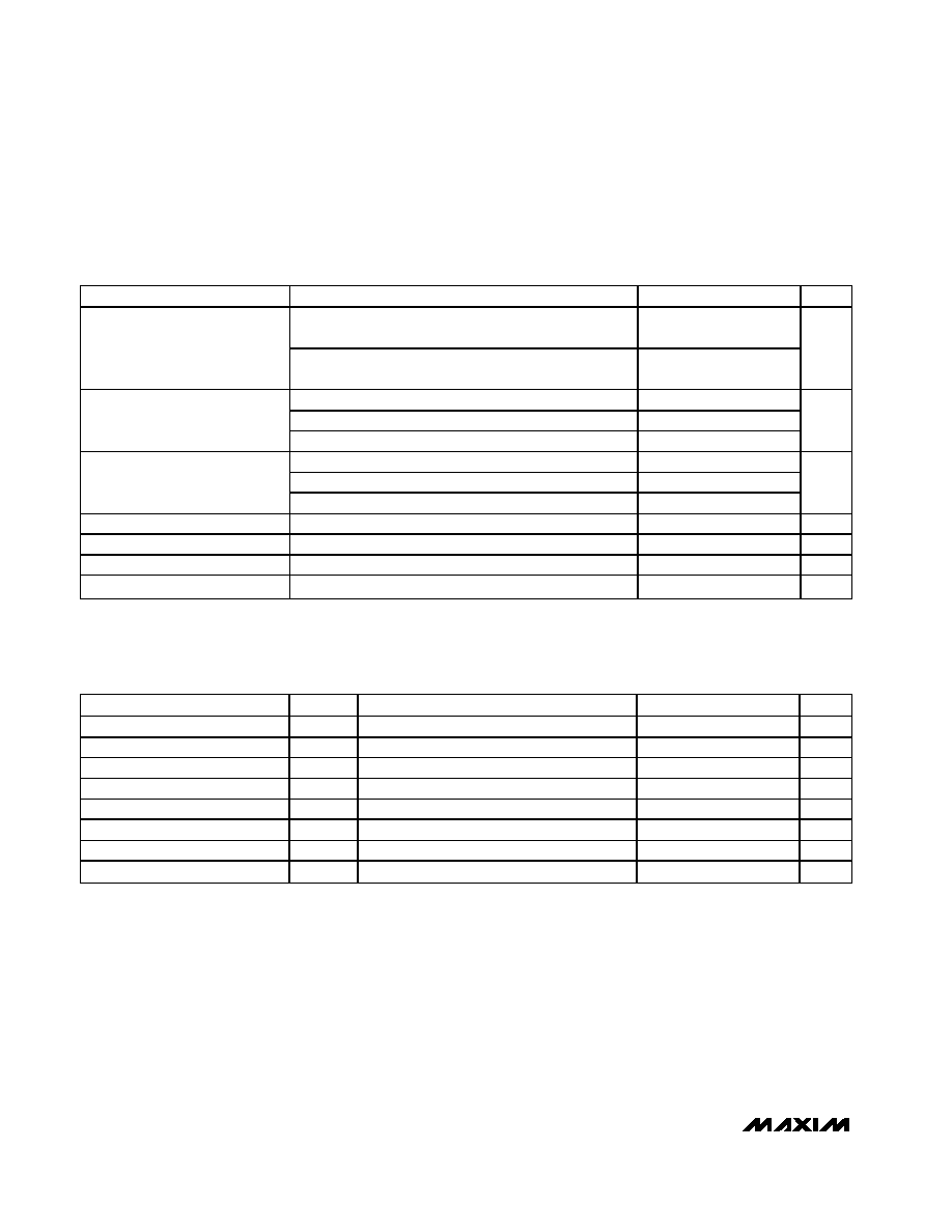
SUPPLY CURRENT
vs. TEMPERATURE
MAX3507 toc01
TEMPERATURE (
∞C)
SUPPLY CURRENT (mA)
NO AC SIGNALS
APPLIED
HP MODE, GC = 127
LN MODE, GC = 80
TXEN = GND
50
110
90
70
130
150
170
190
210
230
250
30
40
50
60
70
SUPPLY CURRENT IN HIGH-POWER MODE
vs. OUTPUT POWER
MAX3507 toc02
P
OUT
(dBmV)
SUPPLY CURRENT (mA)
NO AC SIGNALS
APPLIED
T
A
= +85
∞C
T
A
= +25
∞C
T
A
= -40
∞C
40
50
60
70
80
90
100
110
120
0
20
10
30
40
50
60
SUPPLY CURRENT IN LOW-NOISE MODE
vs. OUTPUT POWER
MAX3507 toc03
P
OUT
(dBmV)
SUPPLY CURRENT (mA)
NO AC SIGNALS APPLIED
T
A
= +85
∞C
T
A
= +25
∞C
T
A
= -40
∞C
31.2
31.5
31.4
31.3
31.6
31.7
31.8
31.9
32.0
32.1
32.2
-40
10
-15
35
60
85
VOLTAGE GAIN IN HIGH-POWER MODE
vs. TEMPERATURE
MAX3507 toc04
TEMPERATURE (
∞C)
VOLTAGE GAIN (dB)
V
CC
= +5.0V
V
CC
= +5.3V
V
CC
= +4.7V
GC = 127
-7.0
-6.8
-6.6
-6.4
-6.2
-6.0
-5.8
-5.6
-5.4
-40
-15
10
35
60
85
VOLTAGE GAIN IN LOW-NOISE MODE
vs. TEMPERATURE
MAX3507 toc05
TEMPERATURE (
∞C)
VOLTAGE GAIN (dB)
V
CC
= 4.7V,
5.0V, 5.3V
GC = 80
-74
-34
-54
6
-14
26
46
1
10
100
1000
VOLTAGE GAIN IN HIGH-POWER MODE
vs. FREQUENCY
MAX3507 toc06
INPUT FREQUENCY (MHz)
VOLTAGE GAIN (dB)
GC = 127
GC = 119
GC = 99
GC = 79
GC = 59
-94
-54
-74
-14
-34
6
26
1
10
100
1000
VOLTAGE GAIN IN LOW-NOISE MODE
vs. FREQUENCY
MAX3507 toc07
INPUT FREQUENCY (MHz)
VOLTAGE GAIN (dB)
GC = 110
GC = 90
GC = 70
GC = 50
-34
-14
-24
6
-4
26
16
36
20
60
80
40
100
120
140
VOLTAGE GAIN vs. GAIN CODE
MAX3507
toc08
GAIN CODE
VOLTAGE GAIN (dB)
HIGH-POWER MODE
LOW-NOISE MODE
0
0.3
0.2
0.1
0.5
0.4
0.9
0.8
0.7
0.6
1.0
60
70
80
90
100
110
120
130
GAIN STEP IN HIGH-POWER MODE
vs. GAIN CODE
MAX3507 toc09
GAIN CODE
G
AIN
S
TEP
(
dB
)
Typical Operating Characteristics
(MAX3507 EV Kit, V
CC
= +5.0V, V
IN
= +34dBmV, TXEN = SHDN = V
CC
, f
IN
= 20MHz, T
A
= +25∞C, unless otherwise noted.)