 | ÐлекÑÑоннÑй компоненÑ: MAX3468 | СкаÑаÑÑ:  PDF PDF  ZIP ZIP |
Äîêóìåíòàöèÿ è îïèñàíèÿ www.docs.chipfind.ru
General Description
The MAX3465MAX3469 are high-speed differential
bus transceivers for RS-485 and RS-422 communica-
tions. They are designed to meet TIA/EIA-422-B,
TIA/EIA-485-A, V.11, and X.27 standards. The trans-
ceiver complies with the Profibus specification provid-
ing +2.1V minimum output level with a 54
load,
40Mbps data rate, and output skew less than 2ns. Each
part contains one three-state differential line driver and
one differential input line receiver. The devices operate
from a +5V supply and feature true fail-safe circuitry,
which guarantees a logic-high receiver output when the
receiver inputs are open or shorted. This enables all
receiver outputs on a terminated bus to output logic
highs when all transmitters are disabled.
All devices feature a 1/4-standard-unit load receiver
input impedance that allows 128 transceivers on the
bus. Driver and receiver propagation delays are guar-
anteed under 20ns for multidrop, clock distribution
applications. Drivers are short-circuit current limited
and are protected against excessive power dissipation
by thermal-shutdown circuitry. The driver and receiver
feature active-high and active-low enables, respective-
ly, that can be connected together externally to serve
as a direction control.
Applications
High-Speed RS-485 Communications
High-Speed RS-422 Communications
Level Translators
Industrial-Control Local Area Networks
Profibus Applications
Features
o Recommended for Profibus Applications
o Up to 40Mbps Data Rate
o 15ns Transmitter Propagation Delay
o 20ns Receiver Propagation Delay
o 2ns Transmitter and Receiver Skew
o High Differential Driver Output Level (2.1V on 54)
o Hot-Swap Versions
o 1µA Shutdown Supply Current
o Low Supply Current Requirements (2.5mA, typ)
o Allow Up to 128 Transceivers on the Bus
o True Fail-Safe Receiver while Maintaining EIA/TIA-
485 Compatibility
o Designed for Multipoint Transmissions on Long
or Noisy Bus Lines
o Full-Duplex and Half-Duplex Versions Available
o Phase Controls to Correct for Twisted-Pair
Reversal for 14-Pin Versions
o Current-Limiting and Thermal Shutdown for
Driver Overload Protection
MAX3465MAX3469
+5V, Fail-Safe, 40Mbps, Profibus RS-485/
RS-422 Transceivers
________________________________________________________________ Maxim Integrated Products
1
Ordering Information
PART
NUMBER
HALF/FULL
DUPLEX
RECEIVER/
DRIVER
ENABLE
LOW-
POWER
SHUTDOWN
HOT SWAP
RECEIVER/
DRIVER PHASE
SELECT
INDEPENDENT
SHDN PIN
PIN COUNT
MAX3465
Full
Yes
Yes
Yes
Yes
Yes
14
MAX3466
Full
Yes
Yes
No
Yes
Yes
14
MAX3467
Full
No
No
No
No
No
8
MAX3468
Half
Yes
Yes
Yes
No
No
8
MAX3469
Half
Yes
Yes
No
No
No
8
Selector Guide
19-3038; Rev 0; 10/03
For pricing, delivery, and ordering information, please contact Maxim/Dallas Direct! at
1-888-629-4642, or visit Maxim's website at www.maxim-ic.com.
Ordering Information continued at end of data sheet.
PART
TEMP RANGE
PIN-PACKAGE
MAX3465CSD
0°C to +70°C
14 SO
MAX3465CPD
0°C to +70°C
14 Plastic DIP
MAX3465ESD
-40°C to +85°C
14 SO
MAX3465EPD
-40°C to +85°C
14 Plastic DIP
Pin Configurations appear at end of data sheet.
MAX3465MAX3469
+5V, Fail-Safe, 40Mbps, Profibus RS-485/
RS-422 Transceivers
2
_______________________________________________________________________________________
ABSOLUTE MAXIMUM RATINGS
ELECTRICAL CHARACTERISTICS
(V
CC
= +5V ±5%, T
A
= T
MIN
to T
MAX
, unless otherwise noted. Typical values are at V
CC
= +5V and T
A
= +25°C.) (Note 1)
Stresses beyond those listed under "Absolute Maximum Ratings" may cause permanent damage to the device. These are stress ratings only, and functional
operation of the device at these or any other conditions beyond those indicated in the operational sections of the specifications is not implied. Exposure to
absolute maximum rating conditions for extended periods may affect device reliability.
Supply Voltage (V
CC
) to GND ..................................-0.3V to +6V
Control Input Voltage (RE, DE, DI, SHDN, TXP, RXP)
to GND....................................................-0.3V to (V
CC
+ 0.3V)
Driver Output Voltage (Y, Z) to GND .........................-8V to +13V
Receiver Input Voltage (A, B) to GND.......................-8V to +13V
Differential Driver Output Voltage (Y - Z) ...............................±8V
Differential Receiver Input (A - B) ..........................................±8V
Receiver Output Voltage (RO) to GND.......-0.3V to (V
CC
+ 0.3V)
Output Driver Current (Y, Z) ...........................................±250mA
Continuous Power Dissipation (T
A
= +70°C)
8-Pin SO (derate 5.88mW/°C above +70°C)................471mW
8-Pin DIP (derate 9.09mW/°C above +70°C) ...............727mW
14-Pin SO (derate 8.33mW/°C above +70°C)..............667mW
14-Pin DIP (derate 10mW/°C above +70°C) ................800mW
Operating Temperature Range
MAX346_C__ ......................................................0°C to +70°C
MAX346_E__....................................................-40°C to +85°C
Junction Temperature ......................................................+150°C
Storage Temperature Range .............................-65°C to +150°C
Lead Temperature (soldering, 10s) .................................+300°C
PARAMETER
SYMBOL
CONDITIONS
MIN
TYP
MAX
UNITS
Power-Supply Range
V
CC
4.75
5.25
V
DRIVER
Differential Driver Output
(No Load)
V
OD
Figure 5, R =
V
CC
V
Differential Driver Output
V
OD
Figure 5, R = 27
2.1
V
Change in Magnitude of
Differential Output Voltage
V
OD
Figure 5, R = 50
or 27 (Note 2)
0.2
V
Driver Common-Mode Output
Voltage
V
OC
Figure 5, R = 50
or 27
3
V
Change in Magnitude of
Common-Mode Voltage
V
OC
Figure 5, R = 50
or 27 (Note 2)
0.2
V
Input High Voltage
V
IH
DE, DI, RE, SHDN
2.0
V
Input Low Voltage
V
IL
DE, DI, RE, SHDN
0.8
V
Input Hysteresis
V
HYS
DE, DI, RE, SHDN
50
mV
V
IN
= +12V
+125
Output Leakage (Y and Z) Full
Duplex
I
O
DE = GND, V
CC
=
GND or +5.25V
V
IN
= -7V
-100
µA
Input Current
I
IN
DI, RE, DE, SHDN
±1
µA
Pulldown Current
RXP = TXP = V
CC
5
15
30
µA
0
V
OUT
+12V, output low
+250
Driver Short-Circuit Output
Current (Note 3)
I
OSD
-7V
V
OUT
V
CC
, output high
-250
mA
(V
CC
- 1V)
V
OUT
+12V, output low
+25
Driver Short-Circuit Foldback
Output Current (Note 3)
I
OSFD
-7V
V
OUT
+1V, output high
+25
mA
Thermal-Shutdown Threshold
140
°C
RECEIVER
Differential Input Capacitance
C
A, B
Between A and B
8
pF
V
IN
= +12V
+250
Input Current (A and B) Full
Duplex
I
A, B
DE = GND,
V
CC
= GND or +5.25V
V
IN
= -7V
-200
µA
MAX3465MAX3469
+5V, Fail-Safe, 40Mbps, Profibus RS-485/
RS-422 Transceivers
_______________________________________________________________________________________
3
ELECTRICAL CHARACTERISTICS (continued)
(V
CC
= +5V ±5%, T
A
= T
MIN
to T
MAX
, unless otherwise noted. Typical values are at V
CC
= +5V and T
A
= +25°C.) (Note 1)
PARAMETER
SYMBOL
CONDITIONS
MIN
TYP
MAX
UNITS
Receiver Differential Threshold
Voltage
V
TH
-7V
V
CM
+12V
-200
-125
-50
mV
Receiver Input Hysteresis
V
TH
V
CM
= 0
20
mV
Receiver Output High Voltage
V
OH
I
O
= -4mA, V
A
- V
B
= V
TH
V
CC
- 1.5
V
Receiver Output Low Voltage
V
OL
I
O
= 4mA, V
B
- V
A
= V
TH
0.4
V
Three-State Output Current at
Receiver
I
OZR
0
V
O
V
CC
±1
µA
Receiver Input Resistance
R
IN
-7V
V
CM
+12V
48
k
Receiver Output Short-Circuit
Current
I
OSR
0
V
RO
V
CC
±7
±95
mA
ESD Protection
A, B, Y, and Z pins
(MAX3467/MAX3468/MAX3469)
±6
kV
SUPPLY CURRENT
N or m al O p er ati on
( S tati c C ond i ti on)
I
Q
No load, DI = V
CC
or DI = GND
2.5
4
mA
Supply Current in SHDN
I
SHDN
DE = GND and RE = V
CC
, or SHDN = V
CC
1
10
µA
SWITCHING CHARACTERISTICS
t
PLH
Driver Propagation Delay
t
PHL
Figures 6 and 7, R
DIFF
= 54
,
C
L
= 50pF
15
ns
t
R
Driver Differential Output Rise or
Fall Time
t
F
Figures 6 and 7, R
DIFF
= 54
,
C
L
= 50pF
10
ns
Driver Output Skew |t
PLH
- t
PHL
|
t
SKEW
Figures 6 and 7, R
DIFF
= 54
,
C
L
= 50pF, TXP = GND or floating
2
ns
Driver Output Transition Skew
Guaranteed by design
1
ns
Maximum Data Rate
30
40
Mbps
Driver Enable to Output High
t
ZH
Figures 8 and 9, S2 closed, R
L
= 500
,
C
L
= 50pF
30
ns
Driver Enable to Output Low
t
ZL
Figures 8 and 9, S1 closed, R
L
= 500
,
C
L
= 50pF
30
ns
Driver Disable Time from Low
t
LZ
Figures 8 and 9, S1 closed, R
L
= 500
,
C
L
= 50pF
30
ns
Driver Disable Time from High
t
HZ
Figures 8 and 9, S2 closed, R
L
= 500
,
C
L
= 50pF
30
ns
Driver Enable Skew Time
|t
ZL -
t
ZH
|
R
L
= 500
, C
L
= 50pF, S1 closed (Figures
8 and 9), output low
5
ns
Driver Disable Skew Time
|t
ZL -
t
ZH
|
R
L
= 500
, C
L
= 50pF, S2 closed (Figures
8 and 9), output high
5
ns
t
PLH
Receiver Propagation Delay
t
PHL
Figure 10, C
L
= 15pF (Note 4)
20
ns
Note 1: All currents into the device are positive; all currents out of the device are negative. All voltages are referenced to device
ground, unless otherwise noted.
Note 2:
V
OD
and
V
OC
are the changes in V
OD
and V
OC
, respectively, when the DI input changes state.
Note 3: The short-circuit output current applies to peak current just prior to foldback-current limiting; the short-circuit foldback output
current applies during current limiting to allow a recovery from bus contention.
Note 4: Capacitive load includes test probe and fixture capacitance.
Note 5: Shutdown is enabled by bringing RE high and DE low or by bringing SHDN high. If the enable inputs are in this state for less
than 50ns, the device is guaranteed not to enter shutdown. If the enable inputs are in this state for at least 800ns, the device
is guaranteed to have entered shutdown.
MAX3465MAX3469
+5V, Fail-Safe, 40Mbps, Profibus RS-485/
RS-422 Transceivers
4
_______________________________________________________________________________________
ELECTRICAL CHARACTERISTICS (continued)
(V
CC
= +5V ±5%, T
A
= T
MIN
to T
MAX
, unless otherwise noted. Typical values are at V
CC
= +5V and T
A
= +25°C.) (Note 1)
PARAMETER
SYMBOL
CONDITIONS
MIN
TYP
MAX
UNITS
Recei ver O utp ut S kew
|t
PLH
-
t
PHL
|
Figure 10, C
L
= 15pF, RXP = GND or
floating (Note 4)
2
ns
Receiver Enable to Output Low
t
ZL
Figures 8 and 11, R
L
= 1k
, C
L
= 15pF,
S1 closed (Note 4)
30
ns
Receiver Enable to Output High
t
ZH
Figures 8 and 11, R
L
= 1k
, C
L
= 15pF,
S2 closed (Note 4)
30
ns
Receiver Disable Time from Low
t
LZ
Figures 8 and 11, R
L
= 1k
, C
L
= 15pF,
S1 closed (Note 4)
30
ns
Receiver Disable Time from High
t
HZ
Figures 8 and 11, R
L
= 1k
, C
L
= 15pF,
S2 closed (Note 4)
30
ns
Time to Shutdown
t
SHDN
(Note 5)
50
800
ns
Driver Enable from Shutdown to
Output High
t
ZH (SHDN)
Figures 8 and 9, R
L
= 500
, C
L
= 50pF,
S2 closed (Note 5)
4
µs
Driver Enable from Shutdown to
Output Low
t
ZL (SHDN)
Figures 8 and 9, R
L
= 500
, C
L
= 50pF,
S1 closed (Note 5)
4
µs
Receiver Enable from Shutdown to
Output High
t
ZH (SHDN)
Figures 8 and 11, R
L
= 1k
, C
L
= 15pF,
S2 closed (Notes 4, 5)
4
µs
Receiver Enable from Shutdown to
Output Low
t
ZL (SHDN)
Figures 8 and 11, R
L
= 1k
, C
L
= 15pF,
S1 closed (Notes 4, 5)
4
µs
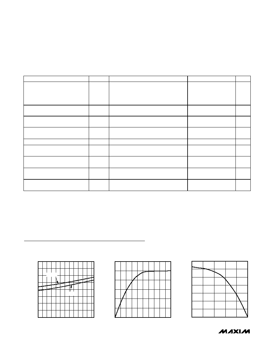
NO-LOAD SUPPLY CURRENT
vs. TEMPERATURE
MAX3465 toc01
TEMPERATURE (
°C)
NO-LOAD SUPPLY CURRENT (mA)
60
40
-20
0
20
2.15
2.20
2.25
2.30
2.35
2.40
2.45
2.50
2.10
-40
80
DE = V
CC
DE = GND
OUTPUT CURRENT
vs. RECEIVER OUTPUT LOW VOLTAGE
MAX3465 toc02
OUTPUT LOW VOLTAGE (V)
OUTPUT CURRENT (mA)
4.5
4.0
3.5
3.0
2.5
2.0
1.5
1.0
0.5
10
20
30
40
50
60
0
0
5.0
OUTPUT CURRENT
vs. RECEIVER OUTPUT HIGH VOLTAGE
MAX3465 toc03
OUTPUT HIGH VOLTAGE (V)
OUTPUT CURRENT (mA)
4
3
2
1
5
10
15
20
25
30
35
0
0
5
Typical Operating Characteristics
(V
CC
= +5V, T
A
= +25°C, unless otherwise noted.)
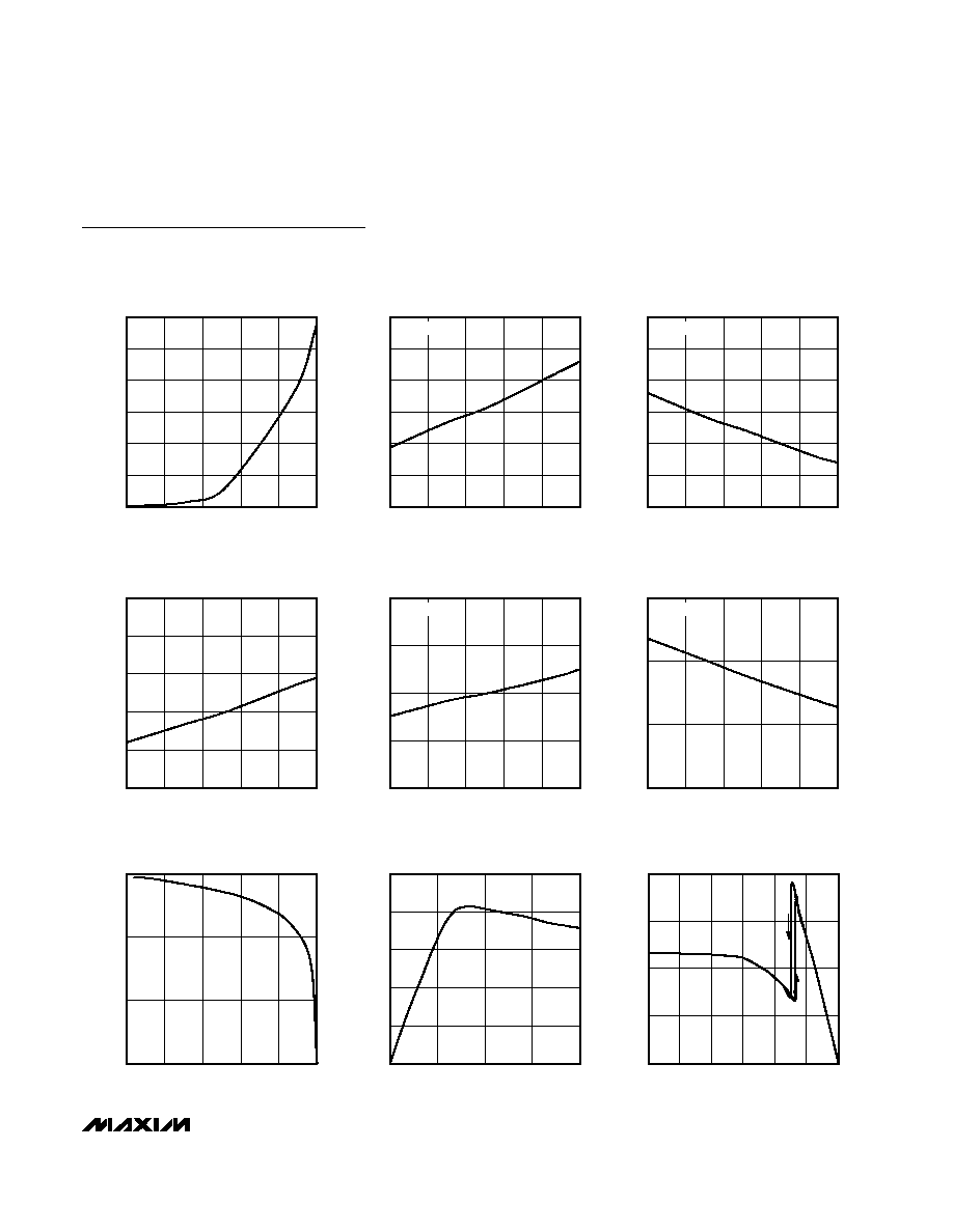
MAX3465MAX3469
+5V, Fail-Safe, 40Mbps, Profibus RS-485/
RS-422 Transceivers
_______________________________________________________________________________________
5
RECEIVER PROPAGATION DELAY
vs. TEMPERATURE
MAX3465 toc07
TEMPERATURE (
°C)
PROPAGATION DELAY (ns)
60
35
10
-15
12
14
16
18
20
10
-40
85
DRIVER PROPAGATION DELAY
vs. TEMPERATURE
MAX3465 toc08
TEMPERATURE (
°C)
PROPAGATION DELAY (ns)
60
35
10
-15
6
8
10
12
4
-40
85
R
DIFF
= 54
DRIVER DIFFERENTIAL OUTPUT VOLTAGE
vs. TEMPERATURE
MAX3465 toc09
TEMPERATURE (
°C)
OUTPUT VOLTAGE (V)
60
35
10
-15
2.5
3.0
3.5
2.0
-40
85
R
DIFF
= 54
DRIVER OUTPUT CURRENT
vs. DIFFERENTIAL OUTPUT VOLTAGE
MAX3465 toc10
DIFFERENTIAL OUTPUT VOLTAGE (V)
OUTPUT CURRENT (mA)
4
3
2
1
1
10
100
0.1
0
5
OUTPUT CURRENT
vs. DRIVER OUTPUT LOW VOLTAGE
MAX3465 toc11
OUTPUT LOW VOLTAGE (V)
OUTPUT CURRENT (mA)
9
6
3
40
80
120
160
200
0
0
12
-160
-120
-80
-40
0
-7
-1
-5
-3
1
3
5
OUTPUT CURRENT
vs. DRIVER OUTPUT HIGH VOLTAGE
MAX3465 toc12
OUTPUT HIGH VOLTAGE (V)
OUTPUT CURRENT (mA)
Typical Operating Characteristics (continued)
(V
CC
= +5V, T
A
= +25°C, unless otherwise noted.)
SHUTDOWN SUPPLY CURRENT
vs. TEMPERATURE
MAX3465 toc04
TEMPERATURE (
°C)
SHUTDOWN SUPPLY CURRENT (nA)
60
35
10
-15
50
100
150
200
250
300
0
-40
85
RECEIVER OUTPUT LOW VOLTAGE
vs. TEMPERATURE
MAX3465 toc05
TEMPERATURE (
°C)
RECEIVER OUTPUT LOW VOLTAGE (mV)
60
35
10
-15
75
100
125
150
175
200
50
-40
85
I
O
= -4mA
RECEIVER OUTPUT HIGH VOLTAGE
vs. TEMPERATURE
MAX3465 toc06
TEMPERATURE (
°C)
RECEIVER OUTPUT HIGH VOLTAGE (mV)
60
35
10
-15
4.65
4.70
4.75
4.80
4.85
4.90
4.60
-40
85
I
O
= 4mA