 | –≠–ª–µ–∫—Ç—Ä–æ–Ω–Ω—ã–π –∫–æ–º–ø–æ–Ω–µ–Ω—Ç: MAX3314 | –°–∫–∞—á–∞—Ç—å:  PDF PDF  ZIP ZIP |
General Description
The MAX3314 is a ±5V powered EIA/TIA-232-compati-
ble interface. It has one transmitter and one receiver in
a flow-through architecture. The transmitter has a low-
dropout output stage providing minimum RS-232-com-
patible ±3.7V output levels while driving 3k
and
1000pf at 460kbps. Both +5V and -5V are supplied
externally.
The MAX3314 has a SHDN function that reduces sup-
ply current to 1µA. The transmitter is disabled and put
into 3-state mode while the receiver remains active.
The MAX3314 is available in 8-pin SOT23, µMAX and
SO packages.
________________________Applications
Digital Cameras
PDA
GPS
POS
Telecommunications
Handy Terminals
Set-Top Boxes
Features
o 1µA Low-Power Shutdown with Receiver Active
o 30µA Operating Supply Current
o 460kbps (min) Data Rate
o 8-Pin SOT23 Package
o RS-232-Compatible Levels
MAX3314
460kbps, 1µA, RS-232-Compatible Transceiver
________________________________________________________________ Maxim Integrated Products
1
RIN
TOUT
TIN
1
2
8
7
GND
V-
SHDN
ROUT
V
CC
SOT23/
µMAX/SO
TOP VIEW
3
4
6
5
MAX3314
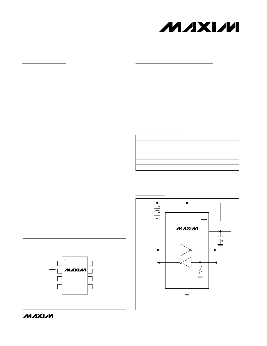
Pin Configuration
C
BYPASS
0.1
µF
2
7
1
8
5
5k
6
4
3
SHDN
V-
TOUT
RIN
TIN
ROUT
V
CC
GND
+5V
MAX3314
CAPACITORS MAY BE POLARIZED OR UNPOLARIZED.
-5V
0.1
µF
Typical Operating Circuit
19-1725; Rev 1a; 3/01
Ordering Information
PART
TEMP. RANGE
PIN-PACKAGE
MAX3314CKA
0
∞C to +70∞C
8 SOT23
MAX3314CUA
0
∞C to +70∞C
8
µMAX
MAX3314CSA
0
∞C to +70∞C
8 SO
MAX3314EKA
-40
∞C to +85∞C
8 SOT23
MAX3314EUA
-40
∞C to +85∞C
8
µMAX
MAX3314ESA
-40
∞C to +85∞C
8 SO
For pricing, delivery, and ordering information, please contact Maxim/Dallas Direct! at
1-888-629-4642, or visit Maxim's website at www.maxim-ic.com.

MAX3314
460kbps, 1µA, RS-232-Compatible Transceiver
2
_______________________________________________________________________________________
ABSOLUTE MAXIMUM RATINGS
ELECTRICAL CHARACTERISTICS
(V
CC
= +5V, V- = -5V, T
A
= T
MIN
to T
MAX
, unless otherwise noted. Typical values are at T
A
= +25∞C.)
Stresses beyond those listed under "Absolute Maximum Ratings" may cause permanent damage to the device. These are stress ratings only, and functional
operation of the device at these or any other conditions beyond those indicated in the operational sections of the specifications is not implied. Exposure to
absolute maximum rating conditions for extended periods may affect device reliability.
Note 1: Not tested--guaranteed by design.
V
CC
to GND ..............................................................-0.3V to +6V
V- to GND .................................................................+0.3V to -6V
Input Voltages
TIN, SHDN to GND ..............................................-0.3V to +6V
RIN to GND .....................................................................±25V
Output Voltages
TOUT to GND...............................................................±13.2V
ROUT ....................................................-0.3V to (V
CC
+ 0.3V)
Short-Circuit Duration
TOUT to GND ........................................................Continuous
Continuous Power Dissipation
8-Pin SOT23 (derate 9.7mW/∞C above +70∞C)...........777mW
8-Pin µMAX (derate 4.1mW/∞C above +70∞C) ............300mW
8-Pin SO (derate 5.88mW/∞C above +70∞C)...............471mW
Operating Temperature Ranges
MAX3314C_A.....................................................0∞C to +70∞C
MAX3314E_A ..................................................-40∞C to +85∞C
Junction Temperature .....................................................+150∞C
Storage Temperature Range ............................-65∞C to +150∞C
Lead Temperature (soldering, 10s) ................................+300∞C
PARAMETER
SYMBOL
CONDITIONS
MIN
TYP
MAX
UNITS
DC CHARACTERISTICS
Positive Supply Operating
Range
V
CC
4.75
5
5.25
V
Negative Supply Operating
Range
V-
-4.75
-5
-5.25
V
Positive Supply Current
SHDN = V
CC
, no load
30
100
µA
Negative Supply Current
SHDN = V
CC
, no load
15
30
µA
Shutdown Supply Current
SHDN = GND
1
10
µA
LOGIC INPUTS (TIN, SHDN)
Input Logic Threshold Low
V
IL
0.8
V
Input Logic Threshold High
V
IH
2.4
V
Transmitter Input Hysteresis
0.5
V
Input Leakage Current
±0.01
µA
RECEIVER OUTPUT
Output Voltage Low
V
OL
I
OUT
= 1.6mA
0.4
V
Output Voltage High
V
OH
I
OUT
= -1.0mA
V
CC
- 0.3
V
CC
- 0.1
V
RECEIVER INPUT
Input Threshold Low
V
IL
0.8
V
Input Threshold High
V
IH
2.4
V
Input Hysteresis
0.5
V
Input Resistance
5
k
TRANSMITTER OUTPUT
Output Voltage Swing
Transmitter output loaded with 3k
to
ground
±3.7
V
Output Resistance (Note 1)
V
CC
= V- = 0, transmitter output =
±2V
300
Output Short-Circuit Current
±60
mA
Output Leakage Current
V
OUT
=
±12V, transmitter disabled
25
µA
MAX3314
460kbps, 1µA, RS-232-Compatible Transceiver
_______________________________________________________________________________________
3
TIMING CHARACTERISTICS
(V
CC
= +5V, V- = -5V, T
A
= T
MIN
to T
MAX
, unless otherwise noted. Typical values are at T
A
= +25∞C.)
PARAMETER
SYMBOL
CONDITIONS
MIN
TYP
MAX
UNITS
Maximum Data Rate
R
L
= 3k
, C
L
=1000pf, transmitter switching
460
kbps
t
PLH
Receiver input to receiver output,
C
L
= 150pF
0.15
Receiver Propagation Delay
t
PHL
Receiver input to receiver output,
C
L
= 150pF
0.15
µs
Transmitter Skew
100
ns
Receiver Skew
50
ns
Transition Region Slew Rate
R
L
= 3k
to 7k, C
L
= 150pF to 1000pF,
measured from +3V to -3V or from -3V to +3V
8
V/µs
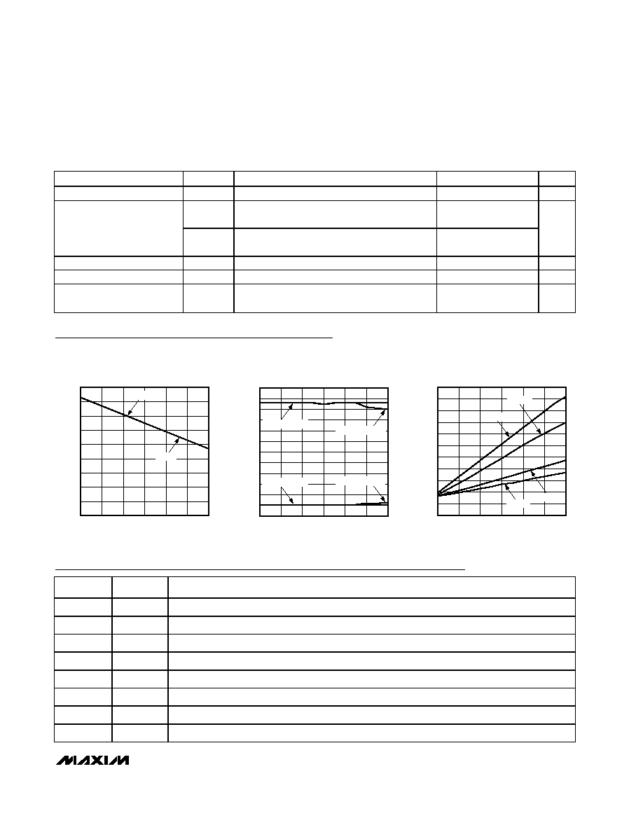
Typical Operating Characteristics
(V
CC
= +5V, V- = -5V, 250kbps data rate, transmitter loaded with 3k
and C
L
, T
A
= +25∞C, unless otherwise noted.)
0
2
1
5
4
3
8
7
6
9
0
1000
500
1500
2000
2500
3000
SLEW RATE vs. LOAD CAPACITANCE
MAX3314-01
LOAD CAPACITANCE (pF)
SLEW RATE (V/us)
SLEW+
SLEW-
-6
-3
-4
-5
1
-1
0
-2
5
3
4
2
6
0
1000
500
1500
2000
2500
3000
TRANSMITTER OUTPUT VOLTAGE
vs. LOAD CAPACITANCE
MAX3314-02
LOAD CAPACITANCE (pF)
TRANSMITTER OUTPUT VOLTAGE (V)
20kbps/120kbps
460kbps/250kbps
460kbps/250kbps
20kbps/120kbps
0
1.5
1.0
0.5
3.0
2.5
2.0
5.0
4.0
4.5
3.5
5.5
0
1000
500
1500
2000
2500
3000
SUPPLY CURRENT
vs. LOAD CAPACITANCE
MAX3314-03
LOAD CAPACITANCE (pF)
SUPPLY CURRENT (mA)
120kbps
20kbps
250kbps
460kbps
Pin Description
PIN
NAME
FUNCTION
1
V
CC
± 5% E xter nal P ow er S up p l y. D ecoup l e w i th a 0.1µF cap aci tor to g r ound .
2
SHDN
Shutdown Active Low. 0 = OFF, 1 = ON.
3
ROUT
TTL/CMOS Receiver Output
4
TIN
TTL/CMOS Transmitter Input
5
TOUT
RS-232-Compatible Transmitter Output
6
RIN
RS-232-Compatible Receiver Input
7
V-
±5% E xter nal P ow er S up p l y. D ecoup l e w i th a 0.1µF cap aci tor to g r ound .
8
GND
Ground

Detailed Description
RS-232-Compatible Drivers
The transmitter is an inverting level translator that con-
verts CMOS-logic levels to EIA/TIA-232-compatible lev-
els. It guarantees data rates up to 460kbps with
worst-case loads of 3k
in parallel with 1000pF. When
SHDN is driven low, the transmitter is disabled and put
into 3-state mode. The transmitter input does not have a
pull-up resistor. Connect to ground if unused.
RS-232-Compatible Receivers
The MAX3314's receiver converts RS-232 signals to
CMOS-logic output levels. The receiver is rated to sig-
nals up to ±25V. The MAX3314's receiver will remain
active during shutdown mode.
MAX3314 Shutdown Mode
In shutdown mode, the transmitter output is put into
high impedance. This reduces the supply current to
1µA. The time required to exit shutdown is less than
2.5µs. Table 1 is the shutdown logic truth table.
Applications Information
Capacitor Selection
The capacitor type used is not critical for proper opera-
tion; either polarized or nonpolarized capacitors are
acceptable. If polarized capacitors are used, connect
polarity as shown in the Typical Operating Circuit.
Bypass V
CC
and V- to ground with at least 0.1µF.
Transmitter Output When
Exiting Shutdown
Figure 1 shows the transmitter output when exiting shut-
down mode. The transmitter is loaded with 3k
in par-
allel with 1000pF. The transmitter output displays no
ringing or undesirable transients as the MAX3314
comes out of shutdown. Note that the transmitter is
enabled only when the magnitude of V- exceeds
approximately -3V.
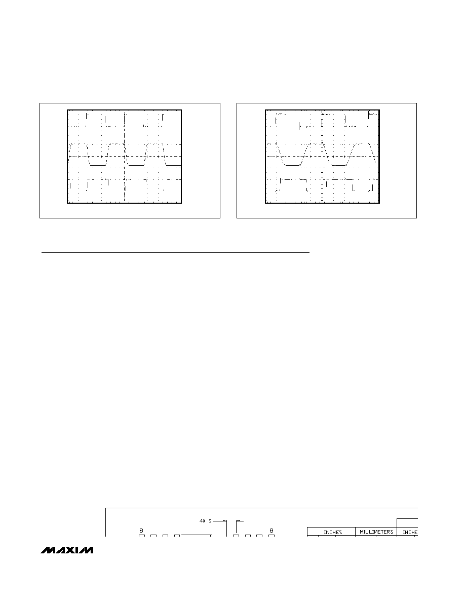
High Data Rates
The MAX3314 maintains minimum RS-232-compatible
±3.7V transmitter output voltage even at high data rates.
Figure 2 shows a transmitter loopback test circuit.
Figure 3 shows the loopback test result at 120kbps, and
Figure 4 shows the same test at 250kbps.
Chip Information
TRANSISTOR COUNT: 128
MAX3314
460kbps, 1µA, RS-232-Compatible Transceiver
4
_______________________________________________________________________________________
SHDN
TRANSMITTER
OUTPUT
RECEIVER
OUTPUT
L
High-Z
Active
H
Active
Active
Table 1. Shutdown Logic Truth Table
Figure 1. Transmitter Output When Exiting Shutdown or
Powering Up
1
µs/div
SHDN
TOUT
5V/div
0
1.5V/div
0
TIN = GND
TIN = V
CC
Figure 2. Loopback Test Circuit
0.1
µF
SHDN
TOUT
RIN
TIN
ROUT
V
CC
GND
5k
+5V
MAX3314
CAPACITORS MAY BE POLARIZED OR NONPOLARIZED.
0.1
µF
-5V
1000pF
V-
MAX3314
460kbps, 1µA, RS-232-Compatible Transceiver
_______________________________________________________________________________________
5
Figure 4. Loopback Test Results at 250kbps
2
µs/div
TOUT
TIN
ROUT
Figure 3. Loopback Test Results at 120kbps
5
µs/div
TOUT
TIN
ROUT
Package Information
Package Information