 | –≠–ª–µ–∫—Ç—Ä–æ–Ω–Ω—ã–π –∫–æ–º–ø–æ–Ω–µ–Ω—Ç: MAX3313E | –°–∫–∞—á–∞—Ç—å:  PDF PDF  ZIP ZIP |
General Description
The MAX3311E/MAX3313E are low-power, 5V EIA/TIA-
232-compatible transceivers. All transmitter outputs
and receiver inputs are protected to ±15kV using the
Human Body Model, making these devices ideal for
applications where more robust transceivers are
required.
Both devices have one transmitter and one receiver.
The transmitters have a proprietary low-dropout trans-
mitter output stage enabling RS-232-compatible opera-
tion from a +5V supply with a single inverting charge
pump. These transceivers require only three 0.1µF
capacitors and will run at data rates up to 460kbps
while maintaining RS-232-compatible output levels.
The MAX3311E features a 1µA shutdown mode. In
shutdown the device turns off the charge pump, pulls
V- to ground, and the transmitter output is disabled.
The MAX3313E features an INVALID output that asserts
high when an active RS-232 cable signal is connected,
signaling to the host that a peripheral is connected to
the communication port.
________________________Applications
Digital Cameras
PDAs
GPS
POS
Telecommunications
Handy Terminals
Set-Top Boxes
Features
o
ESD Protection for RS-232-Compatible I/O Pins
±15kV--Human Body Model
o
1µA Low-Power Shutdown (MAX3311E)
o
INVALID
Output (MAX3313E)
o
Receiver Active in Shutdown (MAX3311E)
o
Single Transceiver (1Tx/1Rx) in 10-Pin µMAX
Package
MAX3311E/MAX3313E
±15kV ESD-Protected, 460kbps, 1µA,
RS-232-Compatible Transceivers in µMAX
________________________________________________________________ Maxim Integrated Products
1
Pin Configurations
19-1910; Rev 0; 1/01
Ordering Information
1
2
3
4
5
10
9
8
7
6
GND
C1+
V-
TOUT
TIN
SHDN
C1-
V
CC
MAX3311E
µ
MAX
TOP VIEW
RIN
ROUT
PART
TEMP. RANGE
PIN-PACKAGE
MAX3311
ECUB
0
∞
C to +70
∞
C
10
µ
MAX
MAX3311EEUB
-40
∞
C to +85
∞
C
10
µ
MAX
MAX3313
ECUB
0
∞
C to +70
∞
C
10
µ
MAX
MAX3313EEUB
-40
∞
C to +85
∞
C
10
µ
MAX
For price, delivery, and to place orders, please contact Maxim Distribution at 1-888-629-4642,
or visit Maxim's website at www.maxim-ic.com.
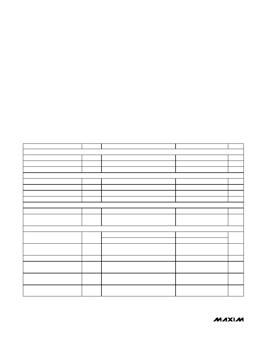
C1
0.1
µ
F
C2
0.1
µ
F
C
BYPASS
0.1
µ
F
9
8
1
10
7
6
3
2
4
5
C1+
V-
TOUT
RIN
C1-
TIN
ROUT
V
CC
GND
5k
SHDN (MAX3311E)
INVALID (MAX3313E)
+5V
MAX3311E
MAX3313E
CAPACITORS MAY BE POLARIZED OR NONPOLARIZED.
Typical Operating Circuit
Pin Configurations continued at end of data sheet.
MAX3311E/MAX3313E
±15kV ESD-Protected, 460kbps, 1µA,
RS-232-Compatible Transceivers in µMAX
2
_______________________________________________________________________________________
ABSOLUTE MAXIMUM RATINGS
ELECTRICAL CHARACTERISTICS
(V
CC
= +5V, C1 and C2 = 0.1µF, T
A
= T
MIN
to T
MAX
. Typical values are at T
A
= +25∞C.)
Stresses beyond those listed under "Absolute Maximum Ratings" may cause permanent damage to the device. These are stress ratings only, and functional
operation of the device at these or any other conditions beyond those indicated in the operational sections of the specifications is not implied. Exposure to
absolute maximum rating conditions for extended periods may affect device reliability.
V
CC
to GND .............................................................-0.3V to +6V
V- to GND ................................................................+0.3V to -7V
V
CC
+ |V-| ............................................................................+13V
Input Voltages
TIN, SHDN to GND ...............................................-0.3V to +6V
RIN to GND ......................................................................±25V
Output Voltages
TOUT to GND................................................................±13.2V
ROUT, INVALID to GND ........................-0.3V to (V
CC
+ 0.3V)
Short-Circuit Duration
TOUT to GND .........................................................Continuous
Continuous Power Dissipation
10-Pin µMAX (derate 5.6mW/∞C above +70∞C) ..........444mW
Operating Temperature Ranges
MAX331_ECUB .................................................0∞C to +70∞C
MAX331_EEUB ..............................................-40∞C to +85∞C
Junction Temperature .....................................................+150∞C
Storage Temperature Range ............................-65∞C to +150∞C
Lead Temperature (soldering, 10s) ................................+300∞C
PARAMETER
SYMBOL
CONDITIONS
MIN
TYP
MAX
UNITS
DC CHARACTERISTICS
Supply Operation Range
V
CC
4.5
5
5.5
V
Supply Current
SHDN = V
CC
, no load
100
250
µ
A
Shutdown Supply Current
SHDN = GND (MAX3311E only)
1
10
µ
A
LOGIC INPUTS (TIN,
SHDN
)
Input Logic Threshold Low
V
IL
0.8
V
Input Logic Threshold High
V
IH
2.4
V
Transmitter Input Hysteresis
0.5
V
Input Leakage Current
±
0.01
±
1
µ
A
RECEIVER OUTPUT
Output Voltage Low
V
OL
I
OUT
= 1.6mA
0.4
V
Output Voltage High
V
OH
I
OUT
= -1.0mA
V
CC
- 0.6
V
CC
- 0.1
V
INVALID
OUTPUT (MAX3313E only)
Figure 7, positive threshold
2.7
Receiver Input Threshold to
INVALID Output High
Figure 7, negative threshold
-2.7
V
Receiver Input Threshold to
INVALID Output Low
Figure 7
-0.3
0.3
V
INVALID Output Low
V
OL
I
OUT
= 1.6mA
0.4
V
INVALID Output High
V
OH
I
OUT
= -1.0mA
V
CC
- 0.6
V
Receiver Positive or Negative
Thresholds to INVALID High
Figure 7
0.1
µ
s
Receiver Positive or Negative
Threshold to INVALID Low
Figure 7
30
µ
s
MAX3311E/MAX3313E
±15kV ESD-Protected, 460kbps, 1µA,
RS-232-Compatible Transceivers in µMAX
_______________________________________________________________________________________
3
ELECTRICAL CHARACTERISTICS (continued)
(V
CC
= +5V, C1 and C2 = 0.1µF, T
A
= T
MIN
to T
MAX
. Typical values are at T
A
= +25∞C.)
TIMING CHARACTERISTICS
(V
CC
= +5V, C1 and C2 = 0.1µF, T
A
= T
MIN
to T
MAX
. Typical values are at T
A
= +25∞C.)
PARAMETER
SYMBOL
CONDITIONS
MIN
TYP
MAX
UNITS
RECEIVER INPUT
Input Threshold Low
V
IL
0.8
V
Input Threshold High
V
IH
2.4
V
Input Hysteresis
0.5
V
Input Resistance
5
k
TRANSMITTER OUTPUT
Output Voltage Swing
Tr ansm i tter outp ut l oad ed w i th 3k
to
±
3.7
V
Output Resistance (Note 1)
V
CC
= 0, transmitter output =
±
2V
300
Output Short-Circuit Current
±
60
mA
Output Leakage Current
V
OUT
=
±
12V, transmitter disabled
±
25
µ
A
ESD PERFORMANCE (TRANSMITTER OUTPUT, RECEIVER INPUT)
ESD-Protection Voltage
Human Body Model
±
15
kV
PARAMETER
SYMBOL
CONDITIONS
MIN
TYP
MAX
UNITS
Maximum Data Rate
R
L
= 3k
, C
L
= 1000pF
460
kbps
Receiver Propagation Delay
t
PLH
/t
PHL
Receiver input to receiver output,
C
L
= 150pF
0.15
µ
s
Transmitter Skew
100
ns
Receiver Skew
50
ns
Transition Region Slew Rate
R
L
= 3k
to 7k
, C
L
= 150pF to 1000pF,
measured from +3V to -3V or from -3V to +3V
11
V/
µ
s
Note 1:
Not tested--guaranteed by design.

MAX3311E/MAX3313E
±15kV ESD-Protected, 460kbps, 1µA,
RS-232-Compatible Transceivers in µMAX
4
_______________________________________________________________________________________
Typical Operating Characteristics
(V
CC
= +5V, 0.1µF capacitors, transmitter loaded with 3k
and C
L
, T
A
= +25∞C, unless otherwise noted.)
0
4
2
8
6
12
10
14
0
1000
1500
500
2000
2500
3000
SLEW RATE
vs. LOAD CAPACITANCE
MAX3311E/13E-01
LOAD CAPACITANCE (pF)
SLEW RATE (V/
µ
s)
+SLEW
250 kbps DATA RATE
-SLEW
-5
-4
-3
-2
-1
0
1
2
3
4
5
6
0
500
1000
1500
2000
2500
3000
TRANSMITTER OUTPUT VOLTAGE
vs. LOAD CAPACITANCE
MAX3311E/13E-02
LOAD CAPACITANCE (pF)
TRANSMITTER OUTPUT VOLTAGE (V)
460kbps/250kbps/120kbps
460kbps/250kbps/120kbps
0
4
2
8
6
12
10
14
0
1000
1500
500
2000
2500
3000
SUPPLY CURRENT
vs. LOAD CAPACITANCE
MAX3311E/13E-03
LOAD CAPACITANCE (pF)
SUPPLY CURRENT (mA)
20kbps
120kbps
250kbps
460kbps
Pin Description
PIN
MAX3311E
MAX3313E
NAME
FUNCTION
1
1
V
CC
+5V External Power Supply. Decouple with a 0.1
µ
F capacitor to ground.
2
2
C1-
Negative Terminal of the Voltage Inverter Charge-Pump Capacitor
3
--
SHDN
Shutdown Active Low (0 = off, 1 = on)
--
3
INVALID
Valid Signal Detector Output, Active Low. A logic high indicates that a valid
RS-232 level is present on the receiver input.
4
4
TIN
TTL/CMOS Transmitter input
5
5
ROUT
TTL/CMOS Receiver output
6
6
RIN
±15kV ESD-Protected, RS-232 Receiver Input
7
7
TOUT
±15kV ESD-Protected, RS-232-Compatible Transmitter Output
8
8
V-
-4.3V generated by the charge pump. Connect a 0.1
µ
F capacitor to ground.
9
9
C1+
Positive Terminal of the Voltage Inverter Charge-Pump Capacitor
10
10
GND
Ground
Detailed Description
Single Charge-Pump Voltage Converter
The MAX3311E/MAX3313E internal power supply has a
single inverting charge pump that provides a negative
voltage from a single +5V supply. The charge pump
operates in a discontinuous mode and requires a flying
capacitor (C1) and a reservoir capacitor (C2) to gener-
ate the V- supply.
RS-232-Compatible Driver
The transmitter is an inverting level translator that con-
verts CMOS-logic levels to EIA/TIA-232 compatible lev-
els. It guarantees data rates up to 460kbps with
worst-case loads of 3k
in parallel with 1000pF. When
SHDN is driven low, the transmitter is disabled and put
into tri-state. The transmitter input does not have an
internal pullup resistor.
RS-232 Receiver
The MAX3311E/MAX3313E receiver converts RS-232
signals to CMOS-logic output levels. The MAX3311E
receiver will remain active during shutdown mode. The
MAX3313E INVALID indicates when an RS-232 signal
is present at the receiver input, and therefore when the
port is in use.
The MAX3313E INVALID output is pulled low when no
valid RS-232 signal level is detected on the receiver
input.
MAX3311E Shutdown Mode
In shutdown mode, the charge pump is turned off, V- is
pulled to ground, and the transmitter output is disabled
(Table 1). This reduces supply current typically to 1µA.
The time required to exit shutdown is less than 25ms.
Applications Information
Capacitor Selection
The capacitor type used for C1 and C2 is not critical for
proper operation; either polarized or nonpolarized
capacitors are acceptable. If polarized capacitors are
used, connect polarity as shown in the Typical
Operating Circuit. The charge pump requires 0.1µF
capacitors. Increasing the capacitor values (e.g., by a
factor of 2) reduces power consumption. C2 can be
increased without changing C1's value. However, do
not increase C1's value without also increasing the
value of C2 and C
BYPASS
to maintain the proper ratios
(C1 to the other capacitors).
When using the minimum 0.1µF capacitors, make sure
the capacitance does not degrade excessively with
temperature. If in doubt, use capacitors with a larger
nominal value. The capacitor's equivalent series resis-
tance (ESR) usually rises at low temperatures and influ-
ences the amount of ripple on V-.
To reduce the output impedance at V-, use larger
capacitors (up to 10µF).
Bypass V
CC
to ground with at least 0.1µF. In applica-
tions sensitive to power-supply noise generated by the
charge pump, decouple V
CC
to ground with a capaci-
tor the same size as (or larger than) charge-pump
capacitors C1 and C2.
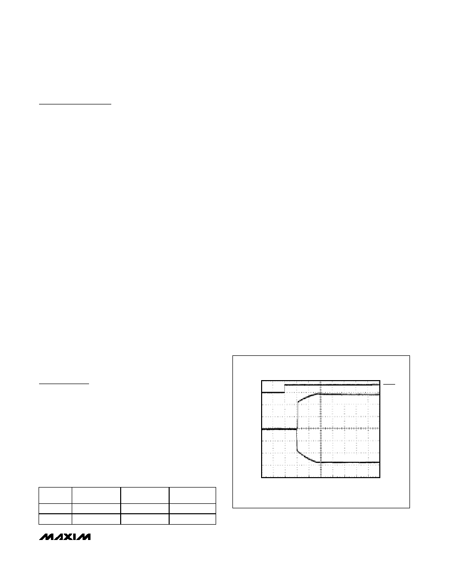
Transmitter Output when Exiting
Shutdown
Figure 1 shows the transmitter output when exiting
shutdown mode. The transmitter is loaded with 3k
in
parallel with 1000pF. The transmitter output displays no
ringing or undesirable transients as the MAX3311E
comes out of shutdown. Note that the transmitter is
enabled only when the magnitude of V- exceeds
approximately -3V.
High Data Rates
The MAX3311E/MAX3313E maintain RS-232-compati-
ble ±3.7V minimum transmitter output voltage even at
MAX3311E/MAX3313E
±15kV ESD-Protected, 460kbps, 1µA,
RS-232-Compatible Transceivers in µMAX
_______________________________________________________________________________________
5
Table 1. MAX3311E Shutdown Logic
Truth Table
SHDN
TRANSMITTER
OUTPUT
RECEIVER
OUTPUT
CHARGE
PUMP
L
High Z
Active
Inactive
H
Active
Active
Active
Figure 1. Transmitter Output when Exiting Shutdown or
Powering Up
10
µ
s/div
SHDN
TOUT
5V/div
0
1.5V/div
0
TIN = GND
TIN = V
CC