 | –≠–ª–µ–∫—Ç—Ä–æ–Ω–Ω—ã–π –∫–æ–º–ø–æ–Ω–µ–Ω—Ç: MAX3291 | –°–∫–∞—á–∞—Ç—å:  PDF PDF  ZIP ZIP |

MAX3291/MAX3292
RS-485/RS-422 Transceivers with Preemphasis
for High-Speed, Long-Distance Communication
________________________________________________________________
Maxim Integrated Products
1
19-1405; Rev 1; 4/99
For free samples & the latest literature: http://www.maxim-ic.com, or phone 1-800-998-8800.
For small orders, phone 1-800-835-8769.
________________General Description
The MAX3291/MAX3292 high-speed RS-485/RS-422
transceivers feature driver preemphasis circuitry, which
extends the distance and increases the data rate of reli-
able communication by reducing intersymbol interfer-
ence (ISI) caused by long cables. The MAX3291 is
programmable for data rates of 5Mbps to 10Mbps,
while the MAX3292 is programmable for data rates up
to 10Mbps by using a single external resistor.
The MAX3291/MAX3292 are full-duplex devices that
operate from a single +5V supply and offer a low-cur-
rent shutdown mode that reduces supply current to
100nA. They feature driver output short-circuit current
limiting and a fail-safe receiver input that guarantees a
logic-high output if the input is open circuit. A 1/4-unit-
load receiver input impedance allows up to 128 trans-
ceivers on the bus.
________________________Applications
Long-Distance, High-Speed RS-485/RS-422
Communications
Telecommunications
Industrial-Control Local Area Networks
____________________________Features
o
Preemphasis Increases the Distance and Data
Rate of Reliable RS-485/RS-422 Communication
o
Data Rate
Optimized for 5Mbps to 10Mbps (MAX3291)
Programmable up to 10Mbps (MAX3292)
o
100nA Low-Current Shutdown Mode
o
Allow Up to 128 Transceivers on the Bus
o
-7V to +12V Common-Mode Input Voltage Range
o
Pin-Compatible with '75180, MAX489, MAX491
MAX3080, MAX3083, MAX3086, MAX1482
2
PEE
(PSET)
12
13
R = Z
O
R = Z
O
R = Z
O
R = Z
O
14
1
1
µ
F
R
PSET
*
C
PSET
*
C
PSET
*
7(6)
GND
11
10
9
( ) ARE FOR MAX3292
* MAX3292 ONLY
Z
O
= THE CHARACTERISTIC
IMPEDANCE OF THE CABLE
RO
RE
DE
DI
3
4
5
9
5
13
7(6)
GND
4
3
DI
DE
RE
RO
2
10
11
12
V
CC
(V
CCD
)
(V
CCD
)
PEE
(PSET)
14
1
1
µ
F
R
PSET
*
V
CC
MAX3291
MAX3292
MAX3291
MAX3292
A
B
Z
Y
Y
Z
B
A
Typical Operating Circuit and Functional Diagram
PART
MAX3291
CSD
MAX3291CPD
MAX3291ESD
-40∞C to +85∞C
0∞C to +70∞C
0∞C to +70∞C
TEMP. RANGE
PIN-PACKAGE
14 SO
14 Plastic DIP
14 SO
_______________Ordering Information
MAX3291EPD
-40∞C to +85∞C
14 Plastic DIP
MAX3292
CSD
MAX3292CPD
MAX3292ESD
-40∞C to +85∞C
0∞C to +70∞C
0∞C to +70∞C
14 SO
14 Plastic DIP
14 SO
MAX3292EPD
-40∞C to +85∞C
14 Plastic DIP
Pin Configuration appears at end of data sheet.
MAX3291/MAX3292
RS-485/RS-422 Transceivers with Preemphasis
for High-Speed, Long-Distance Communication
2
_______________________________________________________________________________________
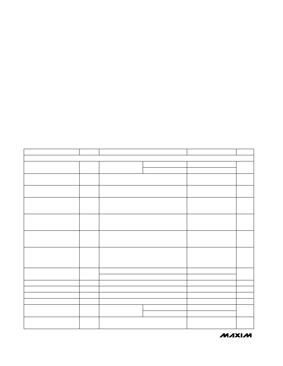
ABSOLUTE MAXIMUM RATINGS
DC ELECTRICAL CHARACTERISTICS
(Typical Operating Circuit, V
CC
= +5V ±5%, R
PSET
= 0 (MAX3292), V
CC
= V
CCD
(MAX3292), T
A
= T
MIN
to T
MAX
, unless otherwise
noted. Typical values are at V
CC
= +5V and T
A
= +25∞C.) (Note 1)
Stresses beyond those listed under "Absolute Maximum Ratings" may cause permanent damage to the device. These are stress ratings only, and functional
operation of the device at these or any other conditions beyond those indicated in the operational sections of the specifications is not implied. Exposure to
absolute maximum rating conditions for extended periods may affect device reliability.
Supply Voltage (V
CC
, V
CCD
) .................................................+6V
Control Input Voltage (RE, DE, PEE,
PSET, DI) .................................................-0.3V to (V
CC
+ 0.3V)
Driver Output Voltage (Y, Z) ................................-7.5V to +12.5V
Receiver Input Voltage (A, B)..............................-7.5V to +12.5V
Receiver Output Voltage (RO)....................-0.3V to (V
CC
+ 0.3V)
Continuous Power Dissipation (T
A
= +70∞C)
14-Pin SO (derate 8.7mW/∞C above +70∞C).................695mW
14-Pin Plastic DIP (derate 10.0mW/∞C above +70∞C) ..800mW
Operating Temperature Ranges
MAX329_C_ D......................................................0∞C to +70∞C
MAX329_E_ D ...................................................-40∞C to +85∞C
Storage Temperature Range .............................-65∞C to +160∞C
Lead Temperature (soldering, 10sec) .............................+300∞C
R = 27
DE = GND,
V
CC
= GND or 5.25V
V
PSET
= V
CC
DE, DI, RE
DE, DI, RE, PEE
DE, DI, RE
CONDITIONS
V
2.4
V
ODP
Differential Driver Output with
Preemphasis
µA
-25
I
O
Output Leakage (Y and Z)
25
µA
70
110
I
PSET
PSET Input Current (MAX3292)
V
2.4
V
IH
Input High Voltage
V
0.8
V
IL
Input Low Voltage
µA
±2
I
IN
Input Current
µA
-15
-30
-45
I
PEE
PEE Input Current (MAX3291)
UNITS
MIN
TYP
MAX
SYMBOL
PARAMETER
Figure 1, R = 27
(Note 3)
V
1.65
2.0
2.35
DPER
Differential Driver
Preemphasis Ratio
Figure 1, R = 27
(Note 4)
V
0.2
V
OD
,
V
ODP
Change in Magnitude of
Differential Output Voltage
(Normal and Preemphasis)
Figure 1, R = 27
V
V
CC
/ 2
3
V
OC
Driver Common-Mode Output
Voltage (Normal and
Preemphasis)
Figure 1, R = 27
(Note 5)
V
0.3
V
OC
Change in Magnitude of
Common-Mode Voltage
(Normal and Preemphasis)
Figure 1, R = 27
mV
50
V
NP
Change in Magnitude of
Common-Mode Output
Voltage (Normal to
Preemphasis)
-7V
V
OUT
+12V (Note 6)
mA
±30
±250
I
OSD
Driver Short-Circuit Output
Current
V
Y
= V
Z
= +12V
V
Y
= V
Z
= -7V
R = 27
Figure 1
No load (Note 2)
V
5.25
V
OD
1.5
5.0
Differential Driver Output
PEE
3.75
DRIVER

MAX3291/MAX3292
RS-485/RS-422 Transceivers with Preemphasis
for High-Speed, Long-Distance Communication
_______________________________________________________________________________________
3
DC ELECTRICAL CHARACTERISTICS (continued)
(Typical Operating Circuit, V
CC
= +5V ±5%, R
PSET
= 0 (MAX3292), V
CC
= V
CCD
(MAX3292), T
A
= T
MIN
to T
MAX
, unless otherwise
noted. Typical values are at V
CC
= +5V and T
A
= +25∞C.) (Note 1)
SWITCHING CHARACTERISTICS
(Typical Operating Circuit, V
CC
= +5V ±5%, R
PSET
= 0 (MAX3292), V
CC
= V
CCD
(MAX3292), T
A
= +25∞C, unless otherwise noted.
Typical values are at V
CC
= +5V and T
A
= +25∞C.)
-7V
V
CM
+12V
RE = V
CC,
DE = GND, V
Y
= V
Z
= 0 to V
CC
or
floating
RE = GND, DE = V
CC
0
V
O
V
CC
-7V
V
CM
+12V
0
V
RO
V
CC
CONDITIONS
mV
-200
200
V
TH
Receiver Differential
Threshold Voltage
µA
0.1
1
I
SHDN
Supply Current in Shutdown
Mode
mA
2.0
3.0
I
CC +
I
CCD
No-Load Supply Current
µA
0.1
±1
I
OZR
Three-State Output Current at
Receiver
k
48
R
IN
Receiver Input Resistance
mA
±15
±95
I
OSR
Receiver Output Short-Circuit
Current
UNITS
MIN
TYP
MAX
SYMBOL
PARAMETER
V
A
= V
B
= 0
mV
35
V
TH
Receiver Input Hysteresis
I
O
= -4mA, V
A
- V
B
= V
TH
V
3.5
V
OH
Receiver Output High Voltage
I
O
= 4mA, V
A
- V
B
= -V
TH
V
0.4
V
OL
Receiver Output Low Voltage
DE = GND,
V
CC
= GND or 5.25V
µA
-150
I
A
,
B
250
Input Current (A and B)
V
IN
= +12V
V
IN
= -7V
Driver Differential Output
Rise or Fall Time
Figures 3 and 5, R
DIFF
= 54
,
C
L1
= C
L2
= 50pF
ns
44
65
t
DPHL
Driver Propagation Delay
CONDITIONS
t
HL
12
Figures 3 and 5, R
DIFF
= 54
,
C
L1
= C
L2
= 50pF
ns
t
LH
Differential Driver Output
Skew
t
DPLH
- t
DPHL
Figures 3 and 10, R
DIFF
= 54
,
C
L1
= C
L2
= 50pF
ns
30
t
PTND
Preemphasis Voltage Level to
Normal Voltage Level Delay
t
DSKEW
Figures 3 and 5, R
DIFF
= 54
,
C
L1
= C
L2
= 50pF
3
8
ns
Mbps
10
f
MAX
Maximum Data Rate
41
65
t
DPLH
UNITS
MIN
TYP
MAX
SYMBOL
PARAMETER
RECEIVER
SUPPLY CURRENT
Driver Preemphasis Interval
t
PRE
80
100
120
Figures 3 and 10,
R
DIFF
= 54
,
C
L1
= C
L2
= 50pF
ns
0.75
1
1.25
µs
MAX3292,
R
PSET
= 523k
MAX3291/MAX3292,
R
PSET
= 0

MAX3291/MAX3292
RS-485/RS-422 Transceivers with Preemphasis
for High-Speed, Long-Distance Communication
4
_______________________________________________________________________________________
SWITCHING CHARACTERISTICS (continued)
(Typical Operating Circuit, V
CC
= +5V ±5%, R
PSET
= 0 (MAX3292), V
CC
= V
CCD
(MAX3292), T
A
= +25∞C, unless otherwise noted.
Typical values are at V
CC
= +5V and T
A
= +25∞C.)
Note 1:
All currents into the device are positive; all currents out of the device are negative. All voltages are referenced to device
ground unless otherwise noted.
Note 2:
Guaranteed by design.
Note 3:
DPER is defined as (V
ODP
/ V
OD
).
Note 4:
V
ODP
and
V
OC
are the changes in V
DD
and V
OC
, respectively, when the DI input changes. This specification reflects
constant operating conditions. When operating conditions shift, the maximum value may be momentarily exceeded.
Note 5:
V
ODP
and
V
OC
are the changes in V
OD
and V
OC
, respectively, when the DI input changes state.
Note 6:
Maximum current level applies to peak current just prior to foldback-current limiting; minimum current level applies during
current limiting.
Note 7:
Shutdown is enabled by bringing RE high and DE low. If the enable inputs are in this state for less than 50ns, the device is
guaranteed not to enter shutdown. If the enable inputs are in this state for at least 500ns, the device is guaranteed to have
entered shutdown. Time to shutdown for the device (t
SHDN
) is measured by monitoring R0 as in Figure 4.
Figures 2 and 6, S2 closed, R
L
= 500
,
C
L
= 100pF
Figures 2 and 6, R
L
= 500
, C
L
= 100pF,
S2 closed
CONDITIONS
ns
ns
6000
8750
t
DZH(SHDN)
Driver Enable from Shutdown
to Output High
UNITS
MIN
TYP
MAX
SYMBOL
PARAMETER
Figures 4 and 11 (Note 7)
ns
50
160
500
t
SHDN
Time to Shutdown
Figures 2 and 8, R
L
= 1k
, C
L
= 100pF,
S1 closed
ns
3
43
55
t
RZL
Receiver Enable to Output
Low
Figures 2 and 8, R
L
= 1k
, C
L
= 15pF,
S1 closed
ns
Figures 2 and 8, R
L
= 1k
, C
L
= 100pF,
S2 closed
25
45
t
RLZ
Receiver Disable Time from
Low
ns
3
43
55
t
RZH
Receiver Enable to Output
High
Figures 2 and 8, R
L
= 1k
, C
L
= 15pF,
S2 closed
ns
25
45
t
RHZ
Receiver Disable Time from
High
Figures 2 and 6, R
L
= 500
, C
L
= 100pF,
S1 closed
ns
6000
8750
t
DZL(SHDN)
Driver Enable from Shutdown
to Output Low
Figures 2 and 8, R
L
= 1k
, C
L
= 100pF,
S1 closed
ns
30
1500
t
RZL(SHDN)
Receiver Enable from
Shutdown to Output Low
Figures 2 and 8, R
L
= 1k
, C
L
= 100pF,
S2 closed
ns
850
1500
t
RZH(SHDN)
Receiver Enable from
Shutdown to Output High
Figures 7 and 9, C
L
= 100pF
ns
3
t
RSKEW
Receiver Output Skew
t
RPLH
- t
RPHL
Driver Enable to Output High
t
DZH
72
105
Figures 7 and 9, C
L
= 50pF, V
ID
= 2V,
V
CM
= 0
Receiver Propagation Delay
t
RPHL
52
85
ns
49
85
t
RPLH
Figures 2 and 6, S2 closed, R
L
= 500
,
C
L
= 15pF
Driver Disable Time from High
t
DHZ
71
100
ns
Figures 2 and 6, S1 closed, R
L
= 500
,
C
L
= 15pF
Driver Disable Time from Low
t
DLZ
53
100
ns
Figures 2 and 6, S1 closed, R
L
= 500
,
C
L
= 100pF
Driver Enable to Output Low
t
DZL
55
105
ns

MAX3291/MAX3292
RS-485/RS-422 Transceivers with Preemphasis
for High-Speed, Long-Distance Communication
_______________________________________________________________________________________
5
TYPICAL PREEMPHASIS WAVEFORM
MAX3291/2-01
100ns/div
V
Y
- V
Z
2V/
div
2500
0
0
1000
PREEMPHASIS INTERVAL vs. R
PSET
(C
PSET
= 0.1
µ
F)
250
500
2250
MAX3291/2-02
R
PSET
(k
)
PREEMPHASIS INTERVAL (ns)
200
100
300 400
600
500
800
700
900
2000
1750
750
1500
1250
1000
NOTE A
0
400
200
800
NOTE A
600
1000
1200
0
1000
500
1500
2000
R
PRE
AND t
PRE
vs. t
BAUD
MAX3291/92 toc 03
t
BAUD
(ns)
R
PRE
(k
)
0
1.0
0.5
2.0
1.5
2.5
3.0
4.0
3.5
4.5
10
30
40
50
20
60
70
80
90 100
DRIVER DIFFERENTIAL
OUTPUT VOLTAGE vs. R
DIFF
MAX3291/2-04
R
DIFF
(
)
DRIVER DIFFERENTIAL OUTPUT VOLTAGE (V)
STRONG
NORMAL
30.0
35.0
32.5
40.0
37.5
42.5
47.5
45.0
50.0
-40
0
20
-20
40
60
80
100
DRIVER PROPAGATION DELAY
vs. TEMPERATURE
MAX3291/2-07
TEMPERATURE (∞C)
PROPAGATION DELAY (ns)
C
L1
= C
L2
= 50pF
2.00
2.50
2.25
3.00
2.75
3.25
3.50
4.00
3.75
4.25
-40
0
20
-20
40
60
80
100
DRIVER DIFFERENTIAL
OUTPUT VOLTAGE vs. TEMPERATURE
MAX3291/2-05
TEMPERATURE (∞C)
DIFFERENTIAL OUTPUT VOLTAGE (V)
STRONG (V
ODP
)
R
DIFF
= 54
NORMAL (V
OD
)
40.0
45.0
42.5
50.0
47.5
52.5
57.5
55.0
60.0
-40
0
20
-20
40
60
80
100
RECEIVER PROPAGATION DELAY
vs. TEMPERATURE
MAX3291/2-06
TEMPERATURE (∞C)
PROPAGATION DELAY (ns)
C
L
= 50pF
RECEIVER PROPAGATION DELAY
MAX3291/2-08
20ns/div
V
A
- V
B
RO
2.5V/
div
5V/
div
__________________________________________Typical Operating Characteristics
(V
CC
= +5V, T
A
= +25∞C, unless otherwise noted.)
Note A:
Dotted line represents region in which preemphasis may not work in systems with excessive power-supply noise. See
Preemphasis at Low Data Rates.