 | ÐлекÑÑоннÑй компоненÑ: MAX2656 | СкаÑаÑÑ:  PDF PDF  ZIP ZIP |
Äîêóìåíòàöèÿ è îïèñàíèÿ www.docs.chipfind.ru
General Description
The MAX2654/MAX2655/MAX2656 high third-order
intercept point (IP3), low-noise amplifiers (LNAs) are
designed for applications in GPS, PCS, WLL, and satel-
lite phone systems. The MAX2654/MAX2655/MAX2656
incorporate on-chip internal output matching to 50
,
eliminating the need for external matching components.
A shutdown feature in the MAX2654/MAX2655 reduces
the operating current to 0.1µA, eliminating the need for
an external supply switch.
The MAX2654 operates in the GPS frequency of
1575MHz with 15.1dB of gain, 1.5dB noise figure, and
only consumes 5.8mA. The MAX2655 is designed with
high-input IP3 to improve operation in cellular applica-
tions where the cellular power amplifier leaks into the
GPS receiver. The MAX2656 is designed for PCS
phone applications with 13.5dB of gain in high-gain
mode and 0.8dB of gain in low-gain mode (selected by
a logic control) and 1.9dB noise figure.
The IP3 of MAX2655/MAX2656 is adjustable by a single
external bias resistor (R
BIAS
), allowing supply current to
be optimized for a specific application.
The MAX2654/MAX2655/MAX2656 operate from a
+2.7V to +5.5V single supply and are available in the
miniature 6-pin SC70 package.
________________________Applications
GPS Receivers
GPS Receivers in Cellular Phones
DCS/PCS Cellular Phones
Satellite Phones
Wireless Local Loop
Features
o Low Noise Figure
MAX2654: 1.5dB at 1575MHz
MAX2655: 1.45dB at 1575MHz
MAX2656: 1.9dB at 1960MHz
o High Gain
MAX2654: 15.1dB at 1575MHz
MAX2655: 14.1dB at 1575MHz
MAX2656: 13.5dB at 1960MHz
o 12.7dB Gain Step (MAX2656 only)
o Integrated 50 Output Matching
o Variable IP3 Set by One Bias Resistor
(MAX2655/MAX2656 only)
o 0.1µA Shutdown Mode (MAX2654/MAX2655 only)
o +2.7V to +5.5V Single-Supply Operation
o Ultra-Small 6-Pin SC70 Package
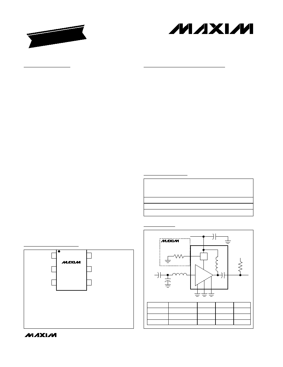
MAX2654/MAX2655/MAX2656
1575MHz/1900MHz Variable-IP3
Low-Noise Amplifiers
________________________________________________________________ Maxim Integrated Products
1
1
6
5
MAX2654
MAX2655
MAX2654
SC70-6
2
3
4
V
CC
RFOUT
ARE FOR MAX2654 ONLY
GND
GND
RFIN
BIAS (GND)
Pin Configuration
MAX2655
MAX2656
C2
3
4
6
10k
Cb
(1)
1
2
5
C1
R
BIAS
V
CTRL
/GND
V
CC
= +3V
RFOUT
RFIN
L1
BIAS
( ) ARE FOR MAX2654 ONLY
Typical Operating Circuit
19-1872; Rev 1; 4/02
EVALUATION KIT
AVAILABLE
Ordering Information
PART
TEMP
RANGE
PIN-
PACKAGE
SOT
TOP-
MARK
MAX2654EXT-T
-40°C to +85°C
6 SC70-6
AAI
MAX2655EXT-T
-40°C to +85°C
6 SC70-6
AAJ
MAX2656EXT-T
-40°C to +95°C
6 SC70-6
AAK
PART
FREQUENCY
L1 (nH)
C1 (pF)
C2 (pF)
MAX2654
1575
5.6
6
1.6
MAX2655
1575
5.6
1800
1.5
MAX2656
1960
4.7
1800
1.2
For pricing, delivery, and ordering information, please contact Maxim/Dallas Direct! at
1-888-629-4642, or visit Maxim's website at www.maxim-ic.com.
MAX2654/MAX2655/MAX2656
1575MHz/1900MHz Variable-IP3
Low-Noise Amplifiers
2
_______________________________________________________________________________________
ABSOLUTE MAXIMUM RATINGS
Stresses beyond those listed under "Absolute Maximum Ratings" may cause permanent damage to the device. These are stress ratings only, and functional
operation of the device at these or any other conditions beyond those indicated in the operational sections of the specifications is not implied. Exposure to
absolute maximum rating conditions for extended periods may affect device reliability.
V
CC
to GND .............................................................-0.3V to +6V
RF Input Power .................................................................+5dBm
Continuous Power Dissipation (T
A
= +70°C)
6-Pin SC70 (derate 3.1mW/°C above +70°C) ..............245mW
Operating Temperature Range ...........................-40°C to +85°C
Maximum Junction Temperature .....................................+150°C
Storage Temperature.........................................-65°C to +150°C
Lead Temperature (soldering, 10s) .................................+300°C
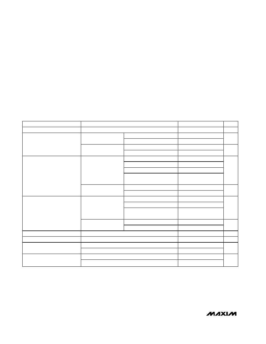
DC ELECTRICAL CHARACTERISTICS
(V
CC
= +2.7V to +5.5V, R
BIAS
= 511
±1%, T
A
= -40°C to +85°C. No RF signal applied. RFIN is AC-coupled and terminated to 50
.
RFOUT is unconnected. Typical values are at V
CC
= +3V, T
A
= +25°C, unless otherwise noted.) (Note 1)
PARAMETER
CONDITIONS
MIN
TYP
MAX
UNIT
Supply Voltage
2.7
5.5
V
T
A
= +25°C
5.8
8.2
V
RFOUT
= V
CC
T
A
= -40°C to +85°C
9.2
mA
T
A
= +25°C
0.1
1
Operating Supply Current
(MAX2654 only)
V
RFOUT
= GND
T
A
= -40°C to +85°C
2.1
µA
R
BIAS
= 511
±1%
8.3
10
R
BIAS
= 698
±1%
5.9
R
BIAS
= 357
±1%
10.1
V
RFOUT
= V
CC
T
A
= +25°C
R
BIAS
= 511
±1%,
T
A
= -40°C to +85°C
11.1
mA
T
A
= +25°C
0.1
1
Operating Supply Current
(MAX2655 only)
V
RFOUT
= GND
T
A
= -40°C to +85°C
2.2
µA
R
BIAS
= 511
±1%
11.5
15.2
R
BIAS
= 715
±1%
8.5
V
RFOUT
= GND
T
A
= +25°C
R
BIAS
= 511
±1%,
T
A
= +85°C
13.6
mA
T
A
= +25°C
12.3
Operating Supply Current
(MAX2656 only)
V
RFOUT
= V
CC
T
A
= +85°C
14.6
mA
Input Logic High at V
RFOUT
(Note 2)
2
V
Input Logic Low at V
RFOUT
(Note 3)
0.6
V
MAX2654/MAX2655
15.6
Input Logic High Current
at V
RFOUT
(Note 4)
MAX2656
71
µA
MAX2654/MAX2655
1
Input Logic Low Current
at V
RFOUT
(Note 5)
MAX2656
-24
µA
MAX2654/MAX2655/MAX2656
1575MHz/1900MHz Variable-IP3
Low-Noise Amplifiers
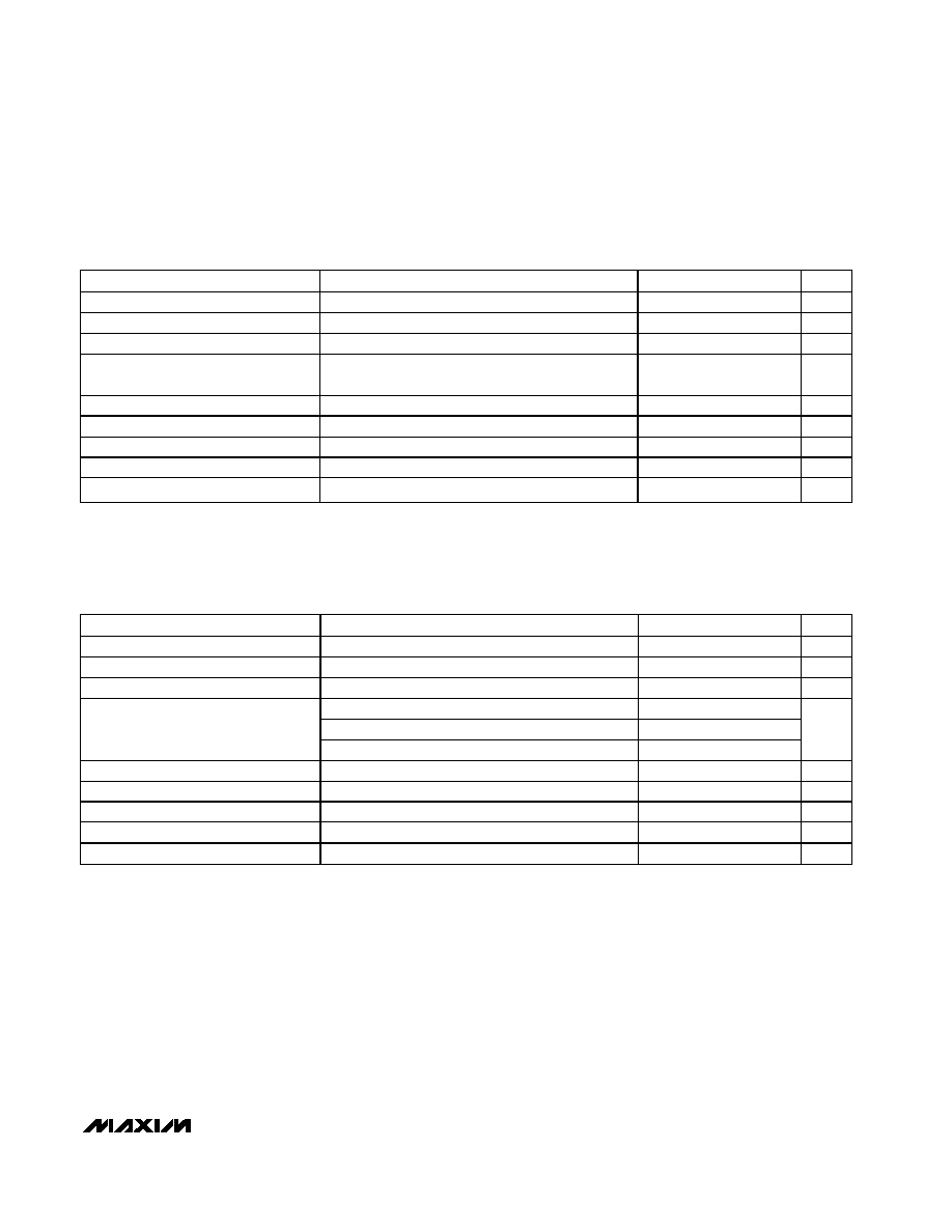
AC ELECTRICAL CHARACTERISTICS (MAX2654)
(MAX2654 Evaluation Kit, V
CC
= +3.0V, P
IN
= -30dBm, f
IN
= 1575MHz, V
RFOUT
= V
CC
through a 10k
resistor, T
A
= +25°C. Typical
values are at V
CC
= +3V, T
A
= +25°C, unless otherwise noted.) (Note 6)
PARAMETER
CONDITIONS
MIN
TYP
MAX
UNIT
Operating Frequency Range (Note 7)
1400
1700
MHz
Gain
(Note 8)
12.7
15.1
dB
Gain Variation Over Temperature
T
A
= -40°C to +85°C
0.15
1
dB
Input Third-Order Intercept Point
(Note 9)
-7.2
dBm
Input 1dB Compression Point
-18
dBm
Noise Figure (Note 10)
1.5
1.8
dB
Input Return Loss
9.7
dB
Output Return Loss
8.4
dB
Reverse Isolation
30
dB
AC ELECTRICAL CHARACTERISTICS (MAX2655)
(MAX2655 Evaluation Kit, V
CC
= +3.0V, P
IN
= -30dBm, f
IN
= 1575MHz, V
RFOUT
= V
CC
through a 10k
resistor, R
BIAS
= 511
±1%,
T
A
= +25°C. Typical values are at V
CC
= +3V, T
A
= +25°C, unless otherwise noted.) (Note 6)
PARAMETER
CONDITIONS
MIN
TYP
MAX
UNIT
Operating Frequency Range (Note 7)
1400
1700
MHz
Gain
(Note 8)
12
14.1
dB
Gain Variation Over Temperature
T
A
= -40°C to +85°C
0.6
1.1
dB
R
BIAS
= 511
±1%
2.8
R
BIAS
= 698
±1%
2.2
dBm
Input Third-Order Intercept Point
(Note 9)
R
BIAS
= 357
±1%
3.8
Input 1dB Compression Point
-12.2
dBm
Noise Figure (Note 10)
1.45
1.9
dB
Input Return Loss
16.1
dB
Output Return Loss
15.5
dB
Reverse Isolation
32
dB
_______________________________________________________________________________________
3
MAX2654/MAX2655/MAX2656
1575MHz/1900MHz Variable-IP3
Low-Noise Amplifiers
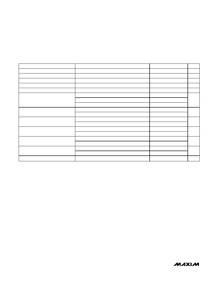
AC ELECTRICAL CHARACTERISTICS (MAX2656)
(MAX2656 Evaluation Kit, V
CC
= +3V, P
IN
= -30dBm, f
IN
= 1960MHz, V
RFOUT
= GND through a 12k
resistor, R
BIAS
= 511
±1%, T
A
= +25°C. Typical values are at V
CC
= +3V, T
A
= +25°C, unless otherwise noted.) (Note 6)
PARAMETER
CONDITIONS
MIN
TYP
MAX
UNIT
Operating Frequency Range (Note 7)
1800
2000
MHz
Gain, High-Gain Mode
(Note 11)
12
13.5
dB
Gain, Low-Gain Mode
(Note 12)
0.8
dB
Gain Variation Over Temperature
T
A
= -40°C to +85°C
0.3
1.2
dB
Gain Step
12.7
dB
R
BIAS
= 511
± 1%
1.5
R
BIAS
= 715
± 1%
-3
Input Third-Order Intercept Point
(Note 13)
Low-gain mode (Note 12)
7.2
dBm
High-gain mode (Note 11)
-7
Input 1dB Compression Point
Low-gain mode (Note 12)
-1.2
dBm
High-gain mode (Note 11)
1.9
2.4
Noise Figure (Note 10)
Low-gain mode (Note 12)
10.8
dB
High-gain mode (Note 11)
14.4
Input Return Loss
Low-gain mode (Note 12)
19.3
dB
High-gain mode (Note 11)
10.7
Output Return Loss
Low-gain mode (Note 12)
7.3
dB
High-gain mode (Note 11)
28
Reverse Isolation
Low-gain mode (Note 12)
25
dB
Gain Step Response Time
3.2
µs
Note 1:
Devices are production tested at T
A
= +25°C. Minimum and maximum values are guaranteed by design and characteriza-
tion over temperature and supply voltages to ±6 sigma.
Note 2:
Minimum DC voltage through a 10k
resistor that sets the MAX2654/MAX2655 to operate in normal mode and MAX2656 in
low-gain mode.
Note 3:
Maximum DC voltage through a 10k
resistor that sets the MAX2654/MAX2655 to operate in shutdown mode and
MAX2656 in high-gain mode.
Note 4:
DC current required when V
RFOUT
is connected to V
CC
through a 10k
resistor.
Note 5:
DC current required when V
RFOUT
is connected to GND through a 10k
resistor.
Note 6:
Guaranteed by design and characterization to ±3 sigma.
Note 7:
The part has been characterized at the specified frequency range. Operation outside of this range is possible, but not
guaranteed.
Note 8:
Production tested at T
A
= +25°C.
Note 9:
Measured with two input tones, f
1
= 1570MHz, f
2
= 1580MHz, both at -30dBm per tone.
Note 10: Excludes PC board losses of 0.2dB for MAX2654/MAX2655 and 0.25dB for MAX2656.
Note 11: High-gain mode is set up by connecting RFOUT to GND through a 12k
resistor.
Note 12: Low-gain mode is set up by connecting RFOUT to V
CC
through a 12k
resistor.
Note 13: Measured with two input tones, f
1
= 1955MHz, f
2
= 1965MHz, both at -30dBm per tone.
4
______________________________________________________________________________________
MAX2654/MAX2655/MAX2656
1575MHz/1900MHz Variable-IP3
Low-Noise Amplifiers
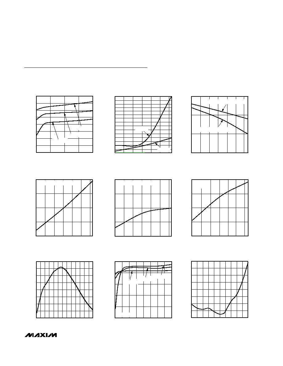
Typical Operating Characteristics
(P
IN
= -30dBm, input and output are terminated to 50
, V
CC
= +3V, high-gain and low-gain modes are applicable only to the MAX2656,
T
A
= +25°C, unless otherwise noted.)
0
1
2
3
4
5
6
7
8
2
3
4
5
6
MAX2654
SUPPLY CURRENT vs. SUPPLY VOLTAGE
MAX2654 toc01
SUPPLY VOLTAGE (V)
SUPPLY CURRENT (mA)
T
A
= -40
°C
T
A
= +25
°C
T
A
= +85
°C
40
45
50
55
60
-40
0
20
-20
40
60
80
MAX2654
INPUT LOGIC CURRENT vs. TEMPERATURE
MAX2654 toc05
TEMPERATURE (
°C)
INPUT LOGIC CURRENT (µA)
INPUT LOGIC LOW AT V
RFOUT
0
6
4
2
8
10
14
12
16
1000 1200
1400
1600 1800
2000
2200
MAX2654
GAIN vs. FREQUENCY
MAX2654 toc07
FREQUENCY (MHz)
GAIN (dB)
1.6
2.0
1.8
2.2
2.8
3.0
2.6
2.4
3.2
1000
1200
1400
1600
1800
2000
MAX2654
NOISE FIGURE vs. FREQUENCY
MAX2654 toc09
FREQUENCY (MHz)
NOISE FIGURE (dB)
0
4
6
7
8
-40
0
20
-20
40
60
80
MAX2654
INPUT LOGIC CURRENT vs. TEMPERATURE
MAX2654 toc04
TEMPERATURE (
°C)
INPUT LOGIC CURRENT (µA)
INPUT LOGIC HIGH AT V
RFOUT
10
11
13
12
14
15
2.0
3.0
3.5
2.5
4.0
4.5
5.0
5.5
6.0
MAX2654
GAIN vs. SUPPLY VOLTAGE
MAX2654 toc08
SUPPLY VOLTAGE (V)
GAIN (dB)
f
0
= 1575MHz
T
A
= +85
°C
T
A
= +25
°C
T
A
= -40
°C
4
6
8
10
12
14
-40
-20
0
20
40
80
60
MAX2654
SHUTDOWN CURRENT vs. TEMPERATURE
MAX2654 toc02
TEMPERATURE (
°C)
SHUTDOWN CURRENT (
µ
A)
2
0
V
CC
= +6V
V
CC
= +3V
-40
0
-20
20
40
60
80
MAX2654
INPUT LOGIC VOLTAGE vs. TEMPERATURE
MAX2654 toc03
TEMPERATURE (
°C)
INPUT LOGIC VOLTAGE (V)
0.5
1.0
1.5
2.0
INPUT LOGIC HIGH AT V
RFOUT
INPUT LOGIC LOW AT V
RFOUT
_______________________________________________________________________________________
5
-10
-9
-8
-7
-6
MAX2654
INPUT IP3 vs. TEMPERATURE
MAX2654 toc06
TEMPERATURE (
°C)
INPUT IP3 (dBm)
-40
20
40
-20
0
60
80
f
1
= 1570 MHz
f
2
= 1580 MHz