MAX1809 DS
General Description
The MAX1809 is a reversible energy flow, constant-off-
time, pulse-width modulated (PWM), step-down DC-DC
converter. It is ideal for use in notebook and subnote-
book computers that require 1.1V to 5V active
termination power supplies. This device features an
internal PMOS power switch and internal synchronous
rectifier for high efficiency and reduced component
count. The internal 90m
PMOS power switch and
70m
NMOS synchronous-rectifier switch easily deliver
continuous load currents up to 3A. The MAX1809 accu-
rately tracks an external reference voltage, produces
an adjustable output from 1.1V to V
IN
, and achieves
efficiencies as high as 93%.
The MAX1809 uses a unique current-mode, constant-
off-time, PWM control scheme that allows the output to
source or sink current. This feature allows energy to
return to the input power supply that otherwise would
be wasted. The programmable constant-off-time archi-
tecture sets switching frequencies up to 1MHz, allowing
the user to optimize performance trade-offs between
efficiency, output switching noise, component size, and
cost. The MAX1809 features an adjustable soft-start to
limit surge currents during startup, a 100% duty-cycle
mode for low-dropout operation, and a low-power shut-
down mode that disables the power switches and
reduces supply current below 1µA. The MAX1809 is
available in a 28-pin QFN with an exposed backside
pad, a 28-pin thin QFN, or a 16-pin QSOP.
Applications
DDR Memory Termination
Active Termination Buses
Features
o Source/Sink 3A
o ±1% Output Accuracy
o Up to 1MHz Switching Frequency
o 93% Efficiency
o Internal PMOS/NMOS Switches
90m
/70m On-Resistance at V
IN
= 4.5V
110m
/80m On-Resistance at V
IN
= 3V
o 1.1V to V
IN
Adjustable Output Voltage
o 3V to 5.5V Input Voltage Range
o <1µA Shutdown Supply Current
o Programmable Constant-Off-Time Operation
o Thermal Shutdown
o Adjustable Soft-Start Inrush Current Limiting
o Output Short-Circuit Protection
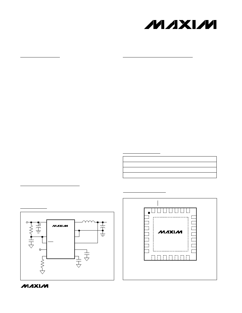
MAX1809
3A, 1MHz, DDR Memory Termination Supply
________________________________________________________________ Maxim Integrated Products
1
IN
N.C.
LX
IN
N.C.
SS
EXTREF
PGND
PGND
LX
LX
PGND
V
CC
GND
N.C.
N.C.
LX
N.C.
LX
N.C.
REF
GND
N.C.
N.C.
N.C.
FB
TOFF
TOP VIEW
THIN QFN
SHDN
28
27
26
25
24
23
22
8
9
10
11
12
13
14
15
16
17
18
19
20
21
7
6
5
4
3
2
1
MAX1809
Pin Configurations
Ordering Information
MAX1809
IN
V
OUT
V
CC
V
IN
V
SET
SHDN
EXTREF
TOFF
LX
PGND
GND
FB
REF
SS
Typical Operating Circuit
19-2142; Rev 1; 9/02
For pricing, delivery, and ordering information, please contact Maxim/Dallas Direct! at
1-888-629-4642, or visit Maxim's website at www.maxim-ic.com.
PART
TEMP RANGE
PIN-PACKAGE
MAX1809EGI*
-40°C to +85°C
28 QFN
MAX1809EEE
-40°C to +85°C
16 QSOP
MAX1809ETI
-40°C to +85°C
28 Thin QFN
Pin Configurations continued at end of data sheet.
*Contact factory for availability.
MAX1809
3A, 1MHz, DDR Memory Termination Supply
2
_______________________________________________________________________________________
ABSOLUTE MAXIMUM RATINGS
ELECTRICAL CHARACTERISTICS
(V
IN
= V
CC
= 3.3V, V
EXTREF
= 1.1V, T
A
= 0°C to +85°C, unless otherwise noted. Typical values are at T
A
= +25°C.)
Stresses beyond those listed under "Absolute Maximum Ratings" may cause permanent damage to the device. These are stress ratings only, and functional
operation of the device at these or any other conditions beyond those indicated in the operational sections of the specifications is not implied. Exposure to
absolute maximum rating conditions for extended periods may affect device reliability.
Note 1: LX has clamp diodes to PGND and IN. If continuous current is applied through these diodes, thermal limits must be
observed.
V
CC
, IN to GND ........................................................-0.3V to +6V
IN to V
CC
.............................................................................±0.3V
GND to PGND.....................................................................±0.3V
SHDN, SS, FB, T
OFF
, R
REF
,
EXTREF to GND.......................................-0.3V to (V
CC
+ 0.3V)
LX Current (Note 1).............................................................±4.7A
REF Short Circuit to GND Duration ............................Continuous
Continuous Power Dissipation (T
A
= +70°C)
28-Pin QFN (derate 20mW/°C above +70°C;
part mounted on 1in
2
of 1oz copper) ..............................1.6W
16-Pin QSOP (derate 12.5mW/°C above +70°C;
part mounted on 1in
2
of 1oz copper) .................................1W
Operating Temperature Range ...........................-40°C to +85°C
Junction Temperature ......................................................+150°C
Storage Temperature Range .............................-65°C to +150°C
Lead Temperature (soldering, 10s) .................................+300°C
PARAMETER
SYMBOL
CONDITIONS
MIN
TYP
MAX
UNITS
Input Voltage
V
IN
,V
CC
3.0
5.5
V
Feedback Voltage Accuracy
(V
FB
- V
EXTREF
)
V
IN
= V
CC
= 3V to 5.5V, I
LOAD
= 0,
V
EXTREF
= 1.25V (Note 2)
-12
+12
mV
Feedback Load Regulation Error
V
FB
I
LOAD
= -3A to +3A, V
EXTREF
= 1.25V
20
mV
External Reference Voltage
Range
V
EXTREF
V
IN
= V
CC
= 3V to 5.5V
V
REF
-
0.01
V
IN
-
1.7
V
Reference Voltage
V
REF
1.078
1.100
1.122
V
Reference Load Regulation
I
REF
= -1µA to +10µA
0.5
2.0
mV
V
IN
= 4.5V
90
200
PMOS Switch
On-Resistance
R
PMOS
I
LX
= 0.5A
V
IN
= 3V
110
250
m
V
IN
= 4.5V
70
150
NMOS Switch
On-Resistance
R
NMOS
I
LX
= 0.5A
V
IN
= 3V
80
200
m
Current-Limit Threshold
I
LIMIT
V
IN
> V
LX
3.5
4.1
4.7
A
Switching Frequency
f
SW
(Note 3)
1
MHz
I
CC
f
SW
= 500kHz
1
No Load Supply Current
I
IN
f
SW
= 500kHz
16
mA
Shutdown Supply Current
I
SHDN
SHDN = GND, I
CC
+ I
IN
<1
15
µA
Thermal-Shutdown Threshold
Hysteresis = 15
°C
160
°C
Undervoltage Lockout Threshold
V
CC
falling, hysteresis = 90mV
2.5
2.6
2.7
V
FB Input Bias Current
I
FB
V
FB
= V
EXTREF
+ 0.1V
0
60
250
nA
R
TOFF
= 30.1k
0.24
0.30
0.37
R
TOFF
= 110k
0.9
1.0
1.1
Off-Time
t
OFF
R
TOFF
= 499k
3.8
4.5
5.2
µs
Startup Off-Time
4 x t
OFF
µs
On-Time
t
ON
(Note 3)
0.35
µs
MAX1809
3A, 1MHz, DDR Memory Termination Supply
_______________________________________________________________________________________
3
ELECTRICAL CHARACTERISTICS
(V
IN
= V
CC
= 3.3V, V
EXTREF
= 1.1V, T
A
= -40°C to +85°C, unless otherwise noted.) (Note 4)
Note 2: The output voltage will have a DC-regulation level lower than the feedback error comparator threshold by 50% of the ripple.
Note 3: Recommended operating frequency, not production tested.
Note 4: Specifications from 0°C to -40°C are guaranteed by design, not production tested.
ELECTRICAL CHARACTERISTICS (continued)
(V
IN
= V
CC
= 3.3V, V
EXTREF
= 1.1V, T
A
= 0°C to +85°C, unless otherwise noted. Typical values are at T
A
= +25°C.)
PARAMETER
SYMBOL
CONDITIONS
MIN
TYP
MAX
UNITS
SS Source Current
I
SS
4
5
6
µA
SS Sink Current
I
SS
V
SS
= 1V
1
50
mA
SHDN Input Current
V
SHDN
= 0, V
CC
-1
+1
µA
V
IL
0.8
SHDN Logic Levels
V
IH
2
V
Maximum Output RMS Current
I
OUT(RMS)
3.1
A
RMS
PARAMETER
SYMBOL
CONDITIONS
MIN
TYP
MAX
UNITS
Input Voltage
V
IN
, V
CC
3.0
5.5
V
Feedback Voltage Accuracy
(V
FB
- V
EXTREF
)
V
IN
= V
CC
= 3V to 5.5V, I
LOAD
= 0,
V
EXTREF
= 1.25V
-24
+24
mV
External Reference Voltage
Range
V
EXTREF
V
IN
= V
CC
= 3 V to 5.5V
V
REF
-
0.01V
V
IN
-
1.9V
V
Reference Voltage
V
REF
1.067
1.133
V
V
IN
= 4.5V
200
PMOS Switch
On-Resistance
R
PMOS
I
LX
= 0.5A
V
IN
= 3V
250
m
V
IN
= 4.5V
150
NMOS Switch
On-Resistance
R
NMOS
I
LX
= 0.5A
V
IN
= 3V
200
m
Current-Limit Threshold
I
LIMIT
V
IN
> V
LX
3.3
4.9
A
FB Input Bias Current
I
FB
V
FB
= V
EXTREF
+ 0.1V
300
nA
Off-Time
t
OFF
R
TOFF
= 110k
0.85
1.15
µs
MAX1809
3A, 1MHz, DDR Memory Termination Supply
4
_______________________________________________________________________________________
50
65
60
55
70
75
80
85
90
95
100
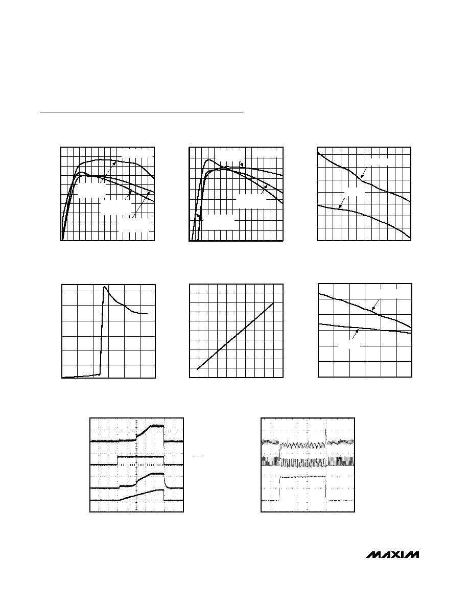
EFFICIENCY vs. OUTPUT CURRENT
(SOURCING)
MAX1809 toc01
OUTPUT CURRENT (A)
EFFICIENCY (%)
0
3
2
1
R
DROOP
= 0
V
IN
= 5V,
V
OUT
= 2.5V
V
IN
= 3.3V,
V
OUT
= 1.25V
V
IN
= 5V,
V
OUT
= 1.25V
EFFICIENCY vs. OUTPUT CURRENT
(SINKING)
MAX1809 toc02
OUTPUT CURRENT (A)
EFFICIENCY (%)
0
3
2
1
50
60
55
75
70
65
90
85
80
95
R
DROOP
= 0
V
IN
= 5V,
V
OUT
= 1.25V
V
IN
= 5V,
V
OUT
= 2.5V
V
IN
= 3.3V,
V
OUT
= 1.25V
-2.2
-2.6
-3.0
-1.8
-1.4
-0.6
-1.0
-0.2
-3
-2
-1
0
1
2
3
NORMALIZED OUTPUT ERROR
vs. OUTPUT CURRENT
MAX1809 toc03
OUTPUT CURRENT (A)
NORMALIZED OUTPUT ERROR (%)
V
IN
= 3.3V
V
IN
= 5V
4
0
12
8
20
16
24
0
2
3
1
4
5
6
NO-LOAD
SUPPLY CURRENT vs. SUPPLY VOLTAGE
MAX1809 toc04
V
IN
(V)
NO-LOAD SUPPLY CURRENT (I
IN
+ I
CC
(mA))
0
1.0
0.5
2.0
1.5
3.0
2.5
3.5
4.5
4.0
5.0
0
100 150 200
50
250 300 350
450
400
500
OFF-TIME vs. R
TOFF
MAX1809 toc05
R
TOFF
(k
)
t
OFF
(
µ
s)
0
400
200
800
600
1000
1200
SWITCHING FREQUENCY
vs. OUTPUT CURRENT
MAX1809 toc06
OUTPUT CURRENT (A)
FREQUECNY (kHz)
-3
-1
-2
0
1
2
3
V
IN
= 5V
V
IN
= 3.3V
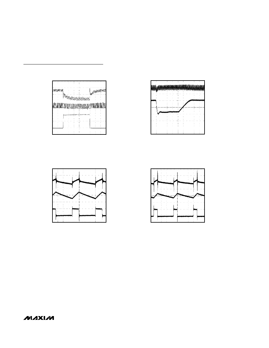
STARTUP AND SHUTDOWN
MAX1809 toc07
0A
0V
0V
0V
1A/div
V
OUT
1V/div
V
SHDN
5V/div
I
IN
1ms/div
V
SS
2V/div
V
IN
= 3.3V, R
OUT
= 0.5
LOAD-TRANSIENT RESPONSE
MAX1809 toc08
0A
0V
50mV/div
I
OUT
5A/div
V(LX)
5V/div
V
OUT
(AC-COUPLED)
10
µs/div
V
EXTREF
= 1.25V, V
IN
= 3.3V, I
OUT
= -2A to +2A to -2A
R
DROOP
= 0
Typical Operating Characteristics
(Circuit of Figure 1, V
OUT
= 1.25V, for V
IN
= 5V: L = 1µH, R
TOFF
= 130k
; for V
IN
= 3.3V: L = 0.68µH, R
TOFF
= 73.2k
.)
MAX1809
3A, 1MHz, DDR Memory Termination Supply
_______________________________________________________________________________________
5
LOAD-TRANSIENT RESPONSE
MAX1809 toc09
0A
0V
50mV/div
I
OUT
5A/div
V(LX)
5V/div
V
OUT
(AC-COUPLED)
10
µs/div
V
EXTREF
= 1.25V, V
IN
= 3.3V, I
OUT
= -2A to +2A to -2A
R
DROOP
12m
LINE-TRANSIENT RESPONSE
MAX1809 toc10
0V
50mV/div
V
IN
2V/div
V
OUT
(AC-COUPLED)
20
µs/div
I
OUT
= 2A, V
IN
= 5V to 3.3V to 5V
SWITCHING WAVEFORMS (SOURCING)
MAX1809 toc11
0V
50mV/div
V(LX)
5V/div
V
OUT
(AC-COUPLED)
400ns/div
I
OUT
= 2A, V
IN
= 5V
I(LX)
2A/div
0A
SWITCHING WAVEFORMS (SINKING)
MAX1809 toc12
0V
50mV/div
V(LX)
5V/div
V
OUT
(AC-COUPLED)
400ns/div
I
OUT
= -2A, V
IN
= 5V
I(LX)
2A/div
0A
Typical Operating Characteristics (continued)
(Circuit of Figure 1, V
OUT
= 1.25V, for V
IN
= 5V: L = 1µH, R
TOFF
= 130k
; for V
IN
= 3.3V: L = 0.68µH, R
TOFF
= 73.2k
.)