 | ÐлекÑÑоннÑй компоненÑ: MAX16803 | СкаÑаÑÑ:  PDF PDF  ZIP ZIP |
Äîêóìåíòàöèÿ è îïèñàíèÿ www.docs.chipfind.ru
General Description
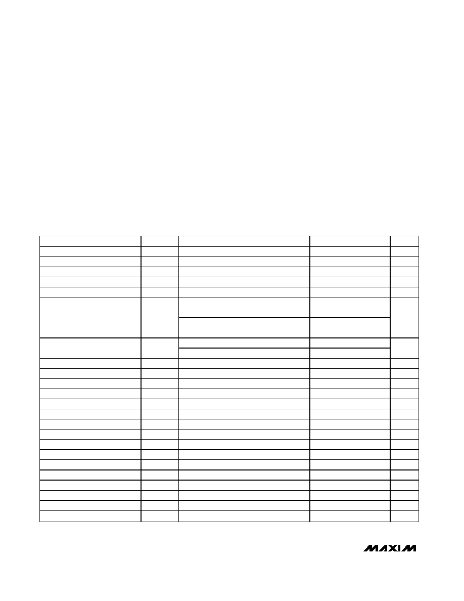
The MAX16803 current regulator operates from a 6.5V
to 40V input-voltage range and delivers up to a total of
350mA to one or more strings of high-brightness LEDs
(HB LEDs). The output current of the MAX16803 is
adjusted by using an external current-sense resistor in
series with the LEDs. A dimming input allows wide-
range "pulsed" PWM operation. Wave-shaping circuitry
reduces EMI. The differential current-sense input
increases noise immunity. The MAX16803 is well suited
for applications requiring high-voltage input and is able
to withstand automotive load-dump events up to 40V.
An on-board pass element minimizes external compo-
nents while providing ±3.5% output-current accuracy.
Additional features include a 5V regulated output and
short-circuit and thermal protection.
The MAX16803 is available in a thermally enhanced,
5mm x 5mm, 16-pin TQFN package and is specified
over the automotive -40°C to +125°C temperature range.
Applications
Automotive Interior: Map, Courtesy, and Cluster
Lighting
Automotive Exterior: Rear Combination Lights (RCLs)
Emergency Vehicle Warning Lights
Navigation and Marine Indicators
General Lighting
Signage, Gasoline Canopies, Beacons
Features
+6.5V to +40V Operating Range
Adjustable LED Current (35mA to 350mA)
±3.5% LED Current Accuracy
High-Voltage DIM Pin for Dimming Interface
Integrated Pass Element with Low-Dropout
Voltage (0.5V typ)
+5V Regulated Output with 4mA Source
Capability
Parallel Operation for LED Current > 350mA
Differential LED Current Sense
Low Shutdown Supply Current (12
µ
A typ)
Low 204mV Current-Sense Reference Reduces
Power Losses
Wave-Shaped Edges Reduce Radiated EMI During
PWM Dimming
Thermal Shutdown
Output Short-Circuit Protection
Available in Small, Thermally Enhanced,
5mm x 5mm, 16-Pin TQFN Package
-40°C to +125°C Operating Temperature Range
MAX16803
High-Voltage, 350mA, High-Brightness LED
Driver with PWM Dimming and 5V Regulator
________________________________________________________________ Maxim Integrated Products
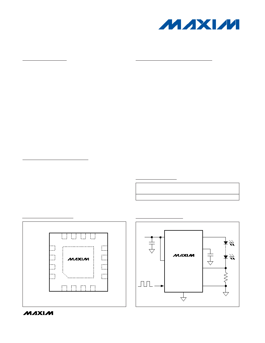
1
15
16
+
14
13
6
5
7
IN
N.C.
8
OUT
V5
CS+
GND
1
2
N.C.
4
12
11
9
EN
OUT
N.C.
N.C.
N.C.
N.C.
MAX16803
IN
CS-
3
10
DIM
TQFN
TOP VIEW
Pin Configuration
Ordering Information
MAX16803
IN
OUT
V5
LEDs
R
SENSE
0.1µF
+6.5V TO +40V
+5V REG
CS+
0.1µF
CS-
DIM
PWM DIMMING
GND
EN
Simplified Diagram
19-0532; Rev 0; 5/06
For pricing, delivery, and ordering information, please contact Maxim/Dallas Direct! at
1-888-629-4642, or visit Maxim's website at www.maxim-ic.com.
+Denotes lead-free package.
*EP = Exposed pad.
PART
TEMP RANGE
PIN-
PACKAGE
PKG
CODE
MAX16803ATE+
-40°C to +125°C
16 TQFN-EP*
T1655-3
MAX16803
High-Voltage, 350mA, High-Brightness LED
Driver with PWM Dimming and 5V Regulator
2
_______________________________________________________________________________________
ABSOLUTE MAXIMUM RATINGS
ELECTRICAL CHARACTERISTICS
(V
IN
= V
EN
= +12V, C
V5
= 0.1µF to GND, I
V5
= 0, V
CS-
= 0V, V
DIM
= +4V, connect R
SENSE
= 0.58 between CS+ and CS- (Note 1).
T
J
= -40°C to +125°C, unless otherwise noted. Typical values are at T
A
= +25°C.) (Note 1)
Stresses beyond those listed under "Absolute Maximum Ratings" may cause permanent damage to the device. These are stress ratings only, and functional
operation of the device at these or any other conditions beyond those indicated in the operational sections of the specifications is not implied. Exposure to
absolute maximum rating conditions for extended periods may affect device reliability.
IN, OUT, DIM, and EN to GND ...............................-0.3V to +45V
CS+, CS-, V5 to GND ...............................................-0.3V to +6V
OUT Short Circuited to GND Duration
(at V
IN
= +16V) ........................................................60 minutes
Maximum Current Into Any Pin (except IN and OUT).........±20mA
Continuous Power Dissipation (T
A
= +70°C)
16-Pin TQFN (derate 33.3mW/
°
C above +70
°
C) ......2666.7mW
Operating Junction Temperature Range ...........-40°C to +125°C
Junction Temperature ......................................................+150°C
Storage Temperature Range .............................-65°C to +150°C
Lead Temperature (soldering, 10s) .................................+300°C
PARAMETER
SYMBOL
CONDITIONS
MIN
TYP
MAX
UNITS
Supply Voltage Range
V
IN
(Note 2)
6.5
40.0
V
Ground Current
I
G
I
LOAD
= 350mA
1.4
3
mA
Shutdown Supply Current
I
SHDN
EN 0.6V
12
40
µA
Guaranteed Output Current
I
OUT
R
SENSE
= 0.55
350
mA
Output Current Accuracy
35mA < I
OUT
< 350mA
±3.5
%
I
OUT
= 350mA (current pulsed),
12V < V
IN
< 40V
0.5
1.2
Dropout Voltage (Note 3)
VDO
I
OUT
= 350mA (current pulsed),
6.5V < V
IN
< 12V
0.5
1.5
V
Current rising, DIM rising to 4V
17
Output Current Slew Rate
Current falling, DIM falling to 0.6V
17
mA/µs
Short-Circuit Current
V
OUT
= 0V, V
IN
= 12V
400
600
800
mA
LOGIC INPUT
EN Input Current
I
EN
100
nA
EN Input Voltage High
V
IH
2.8
V
EN Input Voltage Low
V
IL
0.6
V
TurnOn Time
t
ON
EN rising edge to 90% of OUT
80
µs
CURRENT SENSE (Note 4)
Regulated R
SENSE
Voltage
V
RSNS
V
SENSE
= V
CS+
- V
CS-
196
203
210
mV
CS- Voltage Range
-0.3
+4.1
V
Input Current (CS+)
V
CS+
= 220mV
+14
µA
Input Current (CS-)
V
CS+
= 220mV
-84
µA
DIM Input Current
1
µA
DIM Input Voltage High
V
IH
4
V
DIM Input Voltage Low
V
IL
0.6
V
Turn-On Time
t
ON
After DIM rising to 4V (Note 5)
52
µs
Turn-Off Time
t
OFF
After DIM falling to 0.6V (Note 5)
38
µs
MAX16803
High-Voltage, 350mA, High-Brightness LED
Driver with PWM Dimming and 5V Regulator
_______________________________________________________________________________________
3
Note 1: All devices 100% production tested at T
A
= +25°C. Limits over the operating temperature range are guaranteed by design.
Note 2: Resistors were added from OUT to CS+ to aid with the power dissipation during testing.
Note 3: Dropout is measured as follows:
Connect R
O
= 27 from OUT to CS+. Connect R
SENSE
= 0.58 from CS+ to CS-. Set V
IN
= +12V (record V
OUT
as V
OUT1
).
Reduce V
IN
until V
OUT
= 0.97 x V
OUT1
(record as V
IN2
and V
OUT2
). V
DO
= V
IN2
- V
OUT2
.
Note 4: I
V5
= 0mA.
Note 5: t
ON
time includes the delay and the rise time needed for I
OUT
to reach 90% of its final value. t
OFF
time is the time needed
for I
OUT
to drop below 10%. See the Typical Operating Characteristics. t
ON
and t
OFF
are tested with 13 from OUT to CST.
Note 6: Current regulation varies with V5 load (see the Typical Operating Characteristics).
Note 7: Thermal shutdown does not function if the output of the 5V reference is shorted to ground.
ELECTRICAL CHARACTERISTICS (continued)
(V
IN
= V
EN
= +12V, C
V5
= 0.1µF to GND, I
V5
= 0, V
CS-
= 0V, V
DIM
= +4V, connect R
SENSE
= 0.58 between CS+ and CS- (Note 1).
T
J
= -40°C to +125°C, unless otherwise noted. Typical values are at T
A
= +25°C.) (Note 1)
PARAMETER
SYMBOL
CONDITIONS
MIN
TYP
MAX
UNITS
THERMAL OVERLOAD
Thermal-Shutdown Temperature
+155
°C
Thermal-Shutdown Hysteresis
23
°C
+5V REGULATOR
Output Voltage Regulation
V5
(Note 6)
5.0
5.27
5.5
V
V5 Short-Circuit Current
V5 = 0V (Note 7)
16
mA
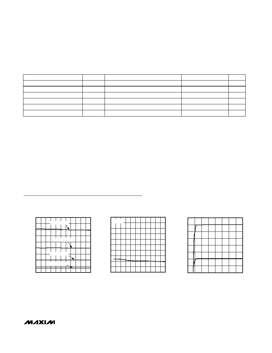
Typical Operating Characteristics
(V
IN
= V
EN
= +12V, T
A
= +25°C, unless otherwise noted.)
OUTPUT CURRENT
vs. TEMPERATURE
MAX16803 toc01
TEMPERATURE (°C)
OUTPUT CURRENT (mA)
110
95
65 80
-10 5
20 35 50
-25
50
100
150
200
250
300
350
400
450
0
-40
125
I
LOAD
= 350mA
I
LOAD
= 35mA
I
LOAD
= 200mA
I
LOAD
= 100mA
(V
CS+
- V
CS-
) vs. OUTPUT CURRENT
MAX16803 toc02
OUTPUT CURRENT (mA)
(V
CS+
- V
CS-
) (V)
320
290
230 260
80 110 140 170 200
50
0.201
0.202
0.203
0.204
0.205
0.206
0.207
0.208
0.209
0.210
0.200
20
350
V
IN
= 12V
OUTPUT CURRENT
vs. INPUT VOLTAGE
MAX16803 toc03
INPUT VOLTAGE (V)
OUTPUT CURRENT (mA)
35
30
5
10
15
20
25
50
100
150
200
250
300
350
400
0
0
40
MAX16803
High-Voltage, 350mA, High-Brightness LED
Driver with PWM Dimming and 5V Regulator
4
_______________________________________________________________________________________
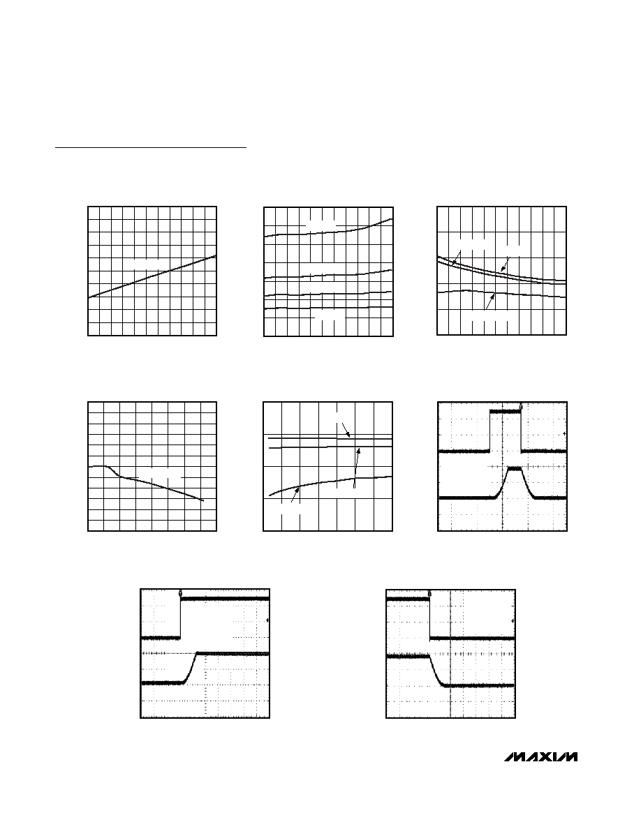
Typical Operating Characteristics (continued)
(V
IN
= V
EN
= +12V, T
A
= +25°C, unless otherwise noted.)
DROPOUT VOLTAGE
vs. TEMPERATURE
MAX16803 toc04
TEMPERATURE (°C)
DROPOUT VOLTAGE (V)
110
95
65 80
-10 5
20 35 50
-25
0.1
0.2
0.3
0.4
0.5
0.6
0.7
0.8
0.9
1.0
0
-40
125
I
LOAD
= 350mA
SHUTDOWN CURRENT
vs. TEMPERATURE
MAX16803 toc05
TEMPERATURE (°C)
SHUTDOWN CURRENT (
µ
A)
110
95
80
65
50
35
20
5
-10
-25
5
10
15
20
25
30
35
0
-40
125
V
IN
= 40V
V
IN
= 20V
V
IN
= 12V
V
IN
= 6.5V
+5V REGULATOR OUTPUT
vs. TEMPERATURE
MAX16803 toc06
TEMPERATURE (°C)
5V REGULATOR OUTPUT (V)
110
95
80
65
50
35
20
5
-10
-25
5.1
5.2
5.3
5.4
5.5
5.0
-40
125
I
LOAD
= 1mA
NO LOAD
I
LOAD
= 5mA
(V
CS+
- V
CS-
) vs. I
V5
MAX16803 toc07
I
V5
(mA)
(V
CS+
- V
CS-
) (V)
7
6
4
5
2
3
1
0.199
0.200
0.201
0.202
0.203
0.204
0.205
0.206
0.207
0.208
0.209
0.210
0.198
0
8
I
LOAD
= 410mA
+5V REGULATOR OUTPUT vs. V
IN
MAX16803 toc08
V
IN
(V)
5V REGULATOR OUTPUT (V)
35
30
25
20
15
10
5.15
5.20
5.25
5.30
5.10
5
40
LOAD = 1mA
NO LOAD
LOAD = 5mA
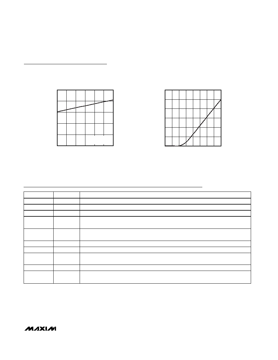
200Hz DIMMED OPERATION
MAX16803 toc09
20µs/div
V
DIM
2V/div
I
LOAD
200mA/div
0A
I
LOAD
= 350mA
V
IN
= V
EN
= 12V
DIM PULSED AT
200Hz (1%
DUTY CYCLE)
0V
200Hz DIMMED OPERATION (EXPANDED)
MAX16803 toc10
20µs/div
V
DIM
2V/div
I
LOAD
200mA/div
0A
I
LOAD
= 350mA
V
IN
= V
EN
= 12V
DIM PULSED AT
200Hz (50%
DUTY CYCLE)
0V
200Hz DIMMED OPERATION (EXPANDED)
MAX16803 toc11
20µs/div
V
DIM
2V/div
I
LOAD
200mA/div
0A
I
LOAD
= 350mA
V
IN
= V
EN
= 12V
DIM PULSED AT
200Hz (50%
DUTY CYCLE)
0V
MAX16803
High-Voltage, 350mA, High-Brightness LED
Driver with PWM Dimming and 5V Regulator
_______________________________________________________________________________________
5
I
DIM
vs. V
DIM
MAX16803 toc13
V
DIM
(V)
I
DIM
(
µ
A)
14
12
10
8
6
4
2
50
100
150
200
250
300
0
0
16
V
SNSE
vs. V
CS-
MAX16803 toc12
V
CS-
(V)
V
SNSE
(mV)
4.5
4.0
3.5
3.0
2.5
201
202
203
204
205
200
2.0
5.0
V
IN
= 12V
I
LOAD
= 350mA
Typical Operating Characteristics (continued)
(V
IN
= V
EN
= +12V, T
A
= +25°C, unless otherwise noted.)
Pin Description
PIN
NAME
FUNCTION
1, 16
OUT
Current-Regulated Output. Connect pin 1 to pin 16.
2, 3
IN
Positive Input Supply. Bypass IN with a 0.1µF (min) capacitor to GND. Connect pin 2 to pin 3.
48, 14
N.C.
Not Internally Connected
9
CS+
Positive Input of the Internal Differential Amplifier. Connect the current-sense resistor between CS+
and CS- to program the output current level.
10
CS-
Negative Input of the Internal Differential Amplifier. Connect the current-sense resistor between
CS- and CS+ to program the output current level.
11
V5
+5V Regulated Output. Connect a 0.1µF capacitor from V5 to GND.
12
GND
Ground
13
DIM
Pulsed Dimming Input. Drive DIM low to disable the output. Drive DIM high to enable the output.
Must not be left unconnected.
15
EN
Enable Input. Drive EN high to enable the output.
--
EP
Exposed Pad. Connect to the ground plane for effective power dissipation. Do not use as the only
ground connection.