 | –≠–ª–µ–∫—Ç—Ä–æ–Ω–Ω—ã–π –∫–æ–º–ø–æ–Ω–µ–Ω—Ç: MAX1611 | –°–∫–∞—á–∞—Ç—å:  PDF PDF  ZIP ZIP |

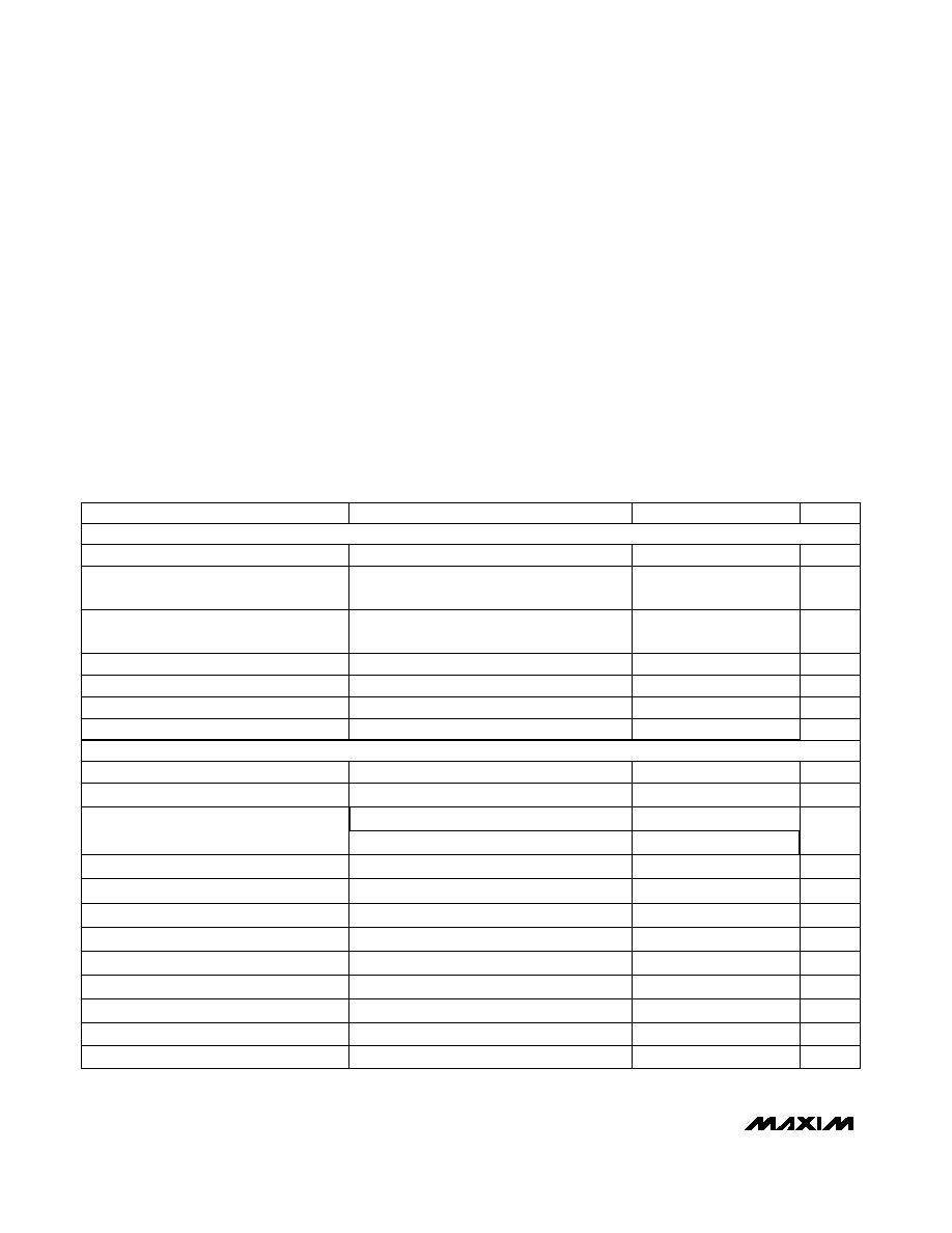
16
15
14
13
12
11
10
9
1
2
3
4
5
6
7
8
BATT
LX
BST
GND
VL
CS
OTP
REF
UP
DN
SHDN
SYNC
SS
CC
CSAV
MINDAC
TOP VIEW
MAX1610
SO
MAX1610/MAX1611
Digitally Controlled CCFL Backlight
Power Supplies
________________________________________________________________
Maxim Integrated Products
1
19-1128; Rev 0; 9/96
EVALUATION KIT
AVAILABLE
For free samples & the latest literature: http://www.maxim-ic.com, or phone 1-800-998-8800
_______________General Description
The MAX1610/MAX1611 are fully integrated, high-
efficiency drivers for cold-cathode fluorescent lamps
(CCFLs). They operate from a 4.5V to 26V power
source. An on-board, high-switching-frequency power
MOSFET reduces external component count and mag-
netics size. The MAX1610/MAX1611 protect against
open or shorted lamps. The CCFL can be driven from
an isolated transformer secondary winding to improve
efficiency and avoid flicker at dim tube settings.
Brightness is adjusted by scaling the lamp current, or
by operating with a fixed lamp current and chopping
the CCFL on and off at a rate faster than the eye can
detect.
The MAX1610's digital inputs increment, decrement, or
clear an internal, 5-bit up/down counter, which sets
CCFL brightness. The MAX1611 uses a System
Management Bus (SMBus) 2-wire serial interface to
directly set CCFL brightness. Both devices include
micropower shutdown and a linear regulator that elimi-
nates the need for a separate logic supply. The digital
interface remains active in shutdown, preserving the
brightness setting.
________________________Applications
Notebook/Laptop Computers
Point-of-Sale Terminals
Portable Medical Equipment
Instrument Displays
____________________________Features
Æ
Direct Digital Control of CCFL Brightness
Æ
Low Supply Current: 3mA Max Operating
20µA Max Shutdown
Æ
Low-Voltage Operation, Down to 4.5V
Æ
Internal 26V, 0.7
W
Power Switch
Æ
Protection Against Open or Shorted Lamps
Æ
Supports Isolated Transformer Secondary
Winding
Æ
SMBus Serial Interface (MAX1611)
Æ
No Flicker at Low Brightness (internal 280Hz
current chopping)
Æ
High Power-to-Light Efficiency
Æ
Selectable 290kHz/145kHz Switching Frequency
Æ
Oscillator SYNC Input
Æ
16-Pin Narrow SO Package
16
15
14
13
12
11
10
9
1
2
3
4
5
6
7
8
BATT
LX
BST
GND
VL
CS
OTP
REF
SDA
SCL
SMBSUS
SYNC
SS
CC
CSAV
MINDAC
MAX1611
SO
__________________________________________________________Pin Configurations
PART
MAX1610
CSE
MAX1611
CSE
0∞C to +70∞C
0∞C to +70∞C
TEMP. RANGE
PIN-PACKAGE
16 Narrow SO
16 Narrow SO
______________Ordering Information
MAX1610/MAX1611
Digitally Controlled CCFL Backlight
Power Supplies
2
_______________________________________________________________________________________
ABSOLUTE MAXIMUM RATINGS
ELECTRICAL CHARACTERISTICS
(T
A
= 0∞C to +70∞C, BATT = 8.2V, MINDAC = 0V, unless otherwise noted. Typical values are at T
A
= +25∞C.)
Stresses beyond those listed under "Absolute Maximum Ratings" may cause permanent damage to the device. These are stress ratings only, and functional
operation of the device at these or any other conditions beyond those indicated in the operational sections of the specifications is not implied. Exposure to
absolute maximum rating conditions for extended periods may affect device reliability.
BATT to GND ............................................................-0.3V to 28V
BST to GND ..............................................................-0.3V to 30V
BST to LX ....................................................................-0.3V to 6V
LX to GND ................................................-0.6V to (BATT + 0.3V)
VL to GND...................................................................-0.3V to 6V
CS, CSAV, CC, SYNC, REF, MINDAC,
SS, OTP to GND............................................-0.3V to (VL + 0.3V)
SHDN, UP, DN to GND ...............................................-0.3V to 6V
SMBSUS, SDA, SCL to GND ......................................-0.3V to 6V
BATT, LX Current .....................................................................1A
SDA Current ........................................................................50mA
VL Current ...........................................................................50mA
Continuous Power Dissipation (T
A
= +70∞C)
SO (derate 8.70mW/∞C above +70∞C) .........................696mW
Operating Temperature Range
MAX1610CSE/MAX1611CSE ..............................0∞C to +70∞C
Storage Temperature Range .............................-65∞C to +160∞C
Lead Temperature (soldering, 10sec) .............................+300∞C
SYNC = REF
SYNC = GND or VL
CONDITIONS
%
89
91
Power-Switch Maximum Duty Cycle
V
4.0
SYNC Input High Voltage
V
0.5
SYNC Input Low Voltage
µ
A
-1
1
SYNC Input Current
ns
200
BATT = 25V
SYNC Low Pulse Width
ns
200
SYNC High Pulse Width
kHz
240
350
Oscillator SYNC Pin Synchronization Range
kHz
125
145
165
4.75V < BATT < 26V
Oscillator Frequency
250
290
330
µ
A
10
No load
LX Switch Off-Leakage Current
0.7
1.0
I
SOURCE
= 100
µ
A
BATT-to-LX Switch On-Resistance
SWITCHING REGULATOR
BST - LX = 4.1V
BATT Input Voltage Range
V
4.75
26
SUPPLY AND REFERENCE
SYNC = REF
mV
6
20
SYNC = GND
REF Load Regulation
V
1.92
2.0
2.08
REF Output Voltage
V
3.0
3.6
4.75
VL Output Voltage, Shutdown Mode
V
4.25
4.5
4.75
VL Output Voltage, Operate Mode
mA
1.5
3
BATT Quiescent Supply Current,
Operate Mode
µ
A
10
20
BATT Quiescent Supply Current,
Shutdown Mode
UNITS
MIN
TYP
MAX
PARAMETER
SS = GND
µ
A
2.5
4.0
5.5
SS Source Current
SS = 0.5V
mA
2
SS Sink Current

MAX1610/MAX1611
Digitally Controlled CCFL Backlight
Power Supplies
_______________________________________________________________________________________
3
ELECTRICAL CHARACTERISTICS (continued)
(T
A
= 0∞C to +70∞C, BATT = 8.2V, MINDAC = 0V, unless otherwise noted. Typical values are at T
A
= +25∞C.)
GND < OTP < VL
Guaranteed monotonic
OTP rising
CONDITIONS
MAX1610 LOGIC LEVELS
mV
500
CS Overcurrent Cutoff Threshold
µ
A
-1
1
OTP Input Bias Current
mV
-20
20
OTP Voltage Trip Point
OPEN AND SHORTED TUBE PROTECTION
µ
A
20
CC Source Current
µ
A
80
D/A at full scale
CC Sink Current
µ
mho
85
CSAV to CC Voltage-to-Current Converter
Transconductance
CC = 2V, CSAV = 1V, D/A at 1LSB
DAC Resolution
Bits
5
CC = 2V, CSAV = 1V, D/A at 1LSB
DAC AND ERROR AMPLIFIER
µ
A
-5
5
CSAV Input Bias Current
mV
232
247
260
CC = 2V, CSAV = 0V, D/A at full scale
CSAV Regulation Point
V
0
1.0
CSAV Input Voltage Range
V
3
MINDAC Digital PWM Threshold
V
0
1
MINDAC Input Voltage Range
µ
A
-1
1
MINDAC Input Bias Current
UNITS
MIN
TYP
MAX
PARAMETER
D/A at 1LSB
12
Referred to REF
V
0.8
SHDN, UP, DN Input Low Voltage
V
2.4
SHDN, UP, DN Input High Voltage
µ
A
-1
1
SHDN, UP, DN Input Bias Current
MAX1611 LOGIC LEVELS
V
0.8
SMBSUS, SDA, SCL Input Low Voltage
V
2.2
SMBSUS, SDA, SCL Input High Voltage
µ
A
-1
1
SMBSUS, SDA, SCL Input Bias Current
V
SDA
= 0.6V
mA
6
SDA Output Low Sink Current
MAX1610/MAX1611
Digitally Controlled CCFL Backlight
Power Supplies
4
_______________________________________________________________________________________
Note 1:
Guaranteed by design.
TIMING CHARACTERISTICS--MAX1611
(Figures 2 and 3, T
A
= +25∞C, unless otherwise noted.)
(Note 1)
(Note 1)
CONDITIONS
µ
s
1
t
R
SCL, SCA Rise Time
µ
s
4.7
t
LOW
µ
s
4
t
HIGH
SCL Serial Clock High Period
SCL Serial Clock Low Period
ns
500
t
SU:DAT
SDA Valid to SCL Rising Edge
Setup Time, Slave Clocking in Data
µ
s
0.3
t
F
SCL, SDA Fall Time
µ
s
4.7
t
SU:STA
Start Condition Setup Time
µ
s
4
t
HD:STA
Start Condition Hold Time
UNITS
MIN
TYP
MAX
SYMBOL
PARAMETER
µ
s
1
t
DV
SCL Falling Edge to SDA Valid,
Reading Out Data
(Note 1)
ns
0
t
HD:DAT
SCL Falling Edge to SDA
Transition
TIMING CHARACTERISTICS--MAX1610
(Figure 1, T
A
= +25∞C, unless otherwise noted.)
CONDITIONS
µ
s
1
t
3
UP, DN Pulse Separation
µ
s
1
t
2
µ
s
1
t
1
UP, DN Pulse Width High
UP, DN Pulse Width Low
µ
s
1
t
4
Counter Reset Time
UNITS
MIN
TYP
MAX
SYMBOL
PARAMETER
MAX1610/MAX1611
Digitally Controlled CCFL Backlight
Power Supplies
_______________________________________________________________________________________
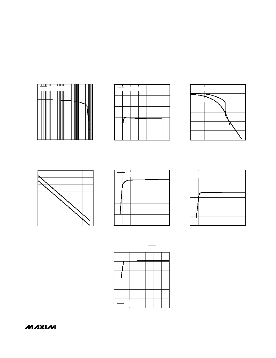
5
1.0
0
BATT SUPPLY CURRENT
vs. BATT VOLTAGE (SHDN = VL)
MAX1610/1611-TOC2
BATT (V)
BATT CURRENT (mA)
1.2
1.4
1.6
1.8
2.0
4
12
16
20
24
28
8
SHDN = VL, OTP = 3V
0
0
BATT SUPPLY CURRENT
vs. BATT VOLTAGE (SHDN = OV)
MAX1610/1611-TOC5
BATT (V)
BATT CURRENT (
µ
A)
2
4
6
8
10
4
12
16
20
24
28
8
SHDN = OV
2.0
0
VL OUTPUT VOLTAGE
vs. BATT VOLTAGE (SHDN = OV)
MAX1610/1611-TOC6
BATT (V)
VL (V)
2.5
3.0
3.5
4.0
4.5
5.0
4
12
16
20
24
28
8
NO LOAD ON VL,
SHDN = OV
2.0
0
VL OUTPUT VOLTAGE
vs. VL OUTPUT CURRENT
MAX1610/1611-TOC3
VL OUTPUT CURRENT (mA)
VL VOLTAGE (V)
2.5
3.0
3.5
4.5
4.0
5.0
20
30
40
10
SHDN = VL, OTP = 3V
BATT = 12V
BATT = 5V
3.30
0
VL OUTPUT VOLTAGE
vs. VL LOAD CURRENT
MAX1610/1611-TOC4
VL LOAD CURRENT (
µ
A)
VL VOLTAGE (V)
3.35
3.40
3.45
3.50
3.55
3.65
3.60
3.70
400
800
600
1000
200
SHDN = GND
BATT = 12V
BATT = 5V
1.5
1
REF OUTPUT VOLTAGE
vs. REF OUTPUT CURRENT
MAX1610/1611-TOC1
REF OUTPUT CURRENT (µA)
REF OUTPUT VOLTAGE (V)
1.6
1.7
1.8
1.9
2.0
2.1
2.2
10
100
1000
10000
SHDN = VL, BATT = 5V
2.0
0
VL OUTPUT VOLTAGE
vs. BATT VOLTAGE (SHDN = VL)
MAX1610/1611-TOC7
BATT (V)
VL (V)
2.5
3.0
3.5
4.0
4.5
5.0
4
12
16
20
24
28
8
NO LOAD ON VL,
SHDN = VL
__________________________________________Typical Operating Characteristics
(T
A
= +25∞C, unless otherwise noted.)