 | ÐлекÑÑоннÑй компоненÑ: MAX1604 | СкаÑаÑÑ:  PDF PDF  ZIP ZIP |
Äîêóìåíòàöèÿ è îïèñàíèÿ www.docs.chipfind.ru
________________General Description
The MAX1601/MAX1604 DC power-switching ICs con-
tain a network of low-resistance MOSFET switches that
deliver selectable VCC and VPP voltages to two
CardBus or PC Card host sockets. Key features include
ultra-low-resistance switches, small packaging, soft-
switching action, and compliance with PCMCIA specifi-
cations for 3V/5V switching. 3.3V-only power switching
for fast, 32-bit CardBus applications is supported in two
ways: stiff, low-resistance 3.3V switches allow high 3.3V
load currents (up to 1A); and completely independent
internal charge pumps let the 3.3V switch operate nor-
mally, even if the +5V and +12V supplies are discon-
nected or turned off to conserve power. The internal
charge pumps are regulating types that draw reduced
input current when the VCC switches are static. Also,
power consumption is automatically reduced to 10µA
max when the switches are programmed to high-Z or
GND states over the serial interface, unlike other solu-
tions that may require a separate shutdown-control
input.
Other key features include guaranteed specifications for
output current limit level, and guaranteed specifications
for output rise/fall times (in compliance with PCMCIA
specifications). Reliability is enhanced by thermal-over-
load protection, accurate current limiting, an overcur-
rent-fault flag output, undervoltage lockout, and extra
ESD protection at the VCC/VPP outputs. The SMBus ser-
ial interface is flexible, and can tolerate logic input levels
in excess of the positive supply rail.
The MAX1604 and MAX1601 are identical, except
for the MAX1604's VY switch, which has roughly three-
times the on-resistance (typically 140m
).The
MAX1601/MAX1604 fit two complete CardBus/PCMCIA
switches into a space-saving, narrow (0.2in. or 5mm
wide) SSOP package.
________________________Applications
Desktop Computers
Data Loggers
Notebook Computers
Digital Cameras
Docking Stations
Printers
Handy-Terminals
PCMCIA Read/Write Drives
____________________________Features
o
Supports Two CardBus Sockets
o
1A, 0.08
Max VY VCC Switch (MAX1601 only)
1A, 0.14
Max VX VCC Switch
o
Soft Switching for Low Inrush Surge Current
o
Overcurrent Protection
o
Overcurrent/Thermal-Fault Flag Output
o
Thermal Shutdown at T
j
= +150°C
o
Independent Internal Charge Pumps
o
Break-Before-Make Switching Action
o
10µA Max Standby Supply Current
o
5V and 12V Not Required for Low-R
DS(ON)
3.3V
Switching
o
Complies with PCMCIA 3V/5V Switching
Specifications
o
Super-Small, 28-Pin SSOP Package
(0.2in. or 5mm wide)
o
System Management Bus (SMBus) Serial
Interface
MAX1601/MAX1604
Dual-Channel CardBus and PCMCIA
Power Switches with SMBusTM Serial Interface
________________________________________________________________
Maxim Integrated Products
1
For free samples & the latest literature: http://www.maxim-ic.com, or phone 1-800-998-8800
19-1085; Rev 1; 10/96
PART
MAX1601
EAI
MAX1604
EAI
-40°C to +85°C
-40°C to +85°C
TEMP. RANGE
PIN-PACKAGE
28 SSOP
28 SSOP
Pin Configuration appears on last page.
SMBus is a trademark of Intel Corp.
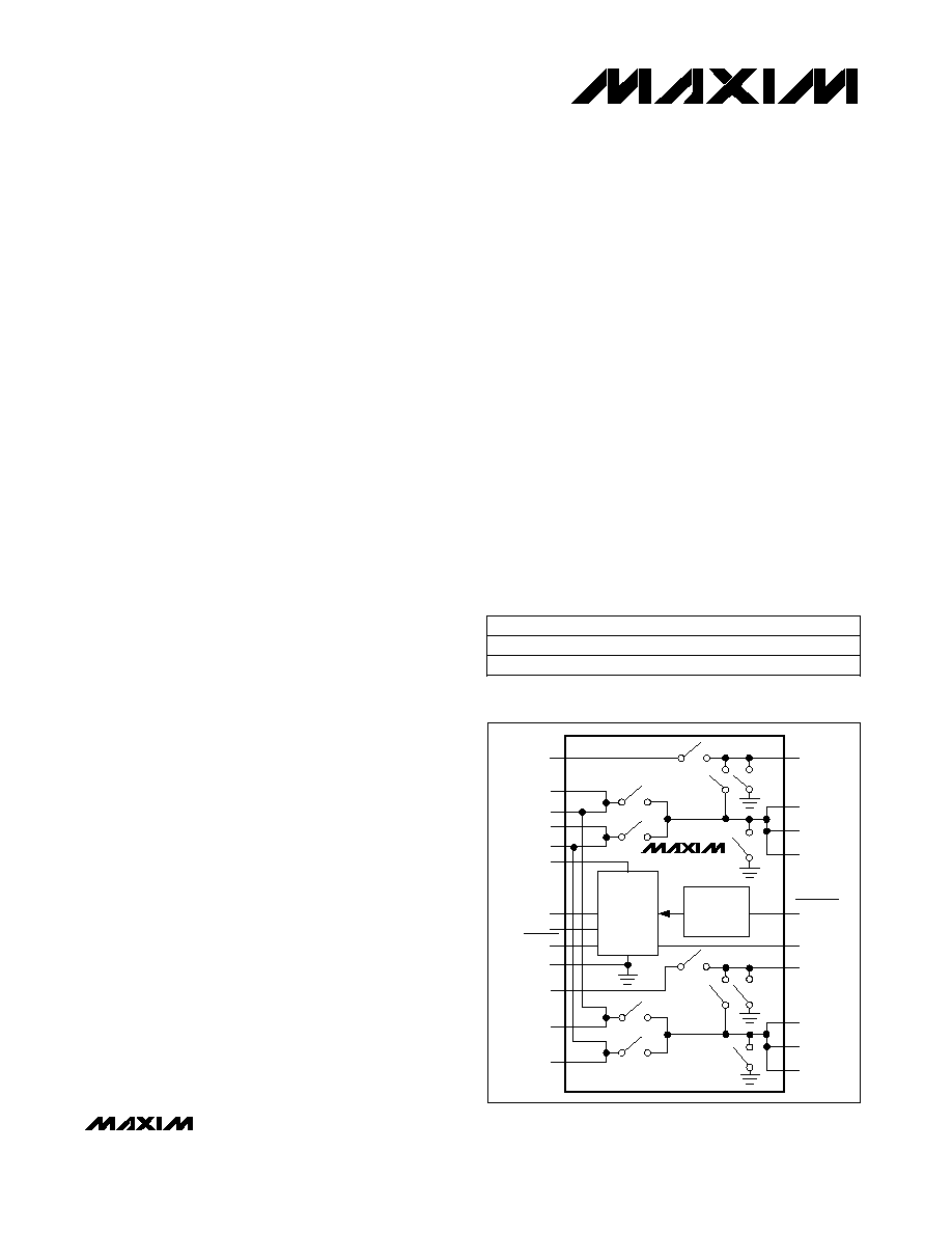
DECODE
LOGIC
VY
12IN
VY
VX
VX
OVERCURRENT
AND
THERMAL
SHUTDOWN
MAX1601/MAX1604
VDD
ADDRESS
SELECT
GND
SMBCLK
SMBDATA
SMBSUS
12IN
VY
VX
VL
VPPA
VCCA
VCCA
VCCA
SMBALERT
ADR
VPPB
VCCB
VCCB
VCCB
__________Simplified Block Diagram
_______________Ordering Information
MAX1601/MAX1604
Dual-Channel CardBus and PCMCIA
Power Switches with SMBusTM Serial Interface
2
_______________________________________________________________________________________
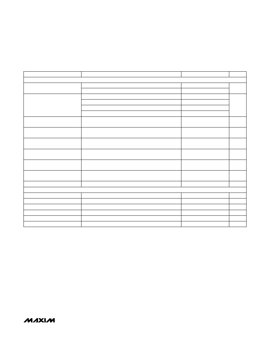
ELECTRICAL CHARACTERISTICS
(VL = VY = 3.3V, VX = 5V, 12INA = 12INB = 12V, T
A
= 0°C to +85°C, unless otherwise noted. Typical values are at T
A
= +25°C.)
Stresses beyond those listed under "Absolute Maximum Ratings" may cause permanent damage to the device. These are stress ratings only, and functional
operation of the device at these or any other conditions beyond those indicated in the operational sections of the specifications is not implied. Exposure to
absolute maximum rating conditions for extended periods may affect device reliability.
2.4
2.5
2.8
V
11
13
Input Voltage Range
µA
25
150
VL Quiescent Supply Current
µA
1
Standby Supply Current
µA
15
100
12IN_ Quiescent Supply Current
µA
4
10
VL Standby Supply Current
UNITS
MIN
TYP
MAX
PARAMETER
VX or VY, all switches 0V or high-Z,
control inputs = 0V or VL, T
A
= +25°C
1
µA
12IN_ Standby Supply Current
3.0
5.5
0.06
0.08
A
0
1
Operating Output Current Range
0.10
0.14
On-Resistance, VX Switches
µA
20
100
VY Quiescent Supply Current
µA
20
100
VX Quiescent Supply Current
V/µs
0.05
VL Fall Rate
1.8
3.0
V
1.4
2.5
2.8
Undervoltage Lockout Threshold
5
8
10
VL falling edge
When using VL as shutdown pin (Note 3)
VX, VY or VL
12INA, 12INB
Any combination of VY switches on,
control inputs = 0V or VL, no VCC loads
MAX1601
VCCA or VCCB, VX = VY = 3V to 5.5V
Any combination of switches on
12INA tied to 12INB, VPPA and VPPB 12V switches on,
control inputs = 0V or VL, no VPP loads
CONDITIONS
12IN falling edge
12INA tied to 12INB, all switches 0V or high-Z,
control inputs = 0V or VL, T
A
= +25°C
12INA = 12INB = 0V to 13V, VX = 4.5V, VY = 0V to 5.5V,
I
SWITCH
= 1A, T
A
= +25°C
Any combination of VX switches on,
control inputs = 0V or high-Z, no VCC loads
12IN rising edge
VX, VY falling edge
12INA = 12INB = 0V to 13V,
VY = 3V, VX = 0V to 5.5V,
I
SWITCH
= 1A, T
A
= +25°C
0.14
0.24
On-Resistance, VY Switches
MAX1604
POWER-SUPPLY SECTION
VCC SWITCHES
All switches 0V or high-Z, control inputs = 0V or VL,
T
A
= +25°C
ABSOLUTE MAXIMUM RATINGS
Note 1:
There are no parasitic diodes between any of these pins, so there are no power-up sequencing restrictions (for example,
logic input signals can be applied even if all of the supply voltage inputs are grounded).
Note 2:
VCC and VPP outputs are internally current-limited to safe values. See the
Electrical Characteristics table.
Inputs/Outputs to GND
(VL, VX, VY, VCCA, VCCB) (Note 1)........................-0.3V, +6V
VPP Inputs/Outputs to GND
(12INA, 12INB, VPPA, VPPB) (Note 1) ..................-0.3V, +15V
Inputs and Outputs to GND (SMBCLK, SMBDATA,
SMBSUS,
SMBALERT) (Note 1) ..............................-0.3V, +6V
ADR Input to GND ...........................................-0.3V, (VL + 0.3V)
VCCA, VCCB Output Current (Note 2).....................................4A
VPPA, VPPB Output Current (Note 2) ...............................250mA
VCCA, VCCB Short Circuit to GND ............................Continuous
VPPA, VPPB Short Circuit to GND..............................Continuous
Continuous Power Dissipation (T
A
= +70°C)
SSOP (derate 9.52mW/°C above +70°C) ....................762mW
Operating Temperature Range
MAX1601EAI/MAX1604EAI .............................-40°C to +85°C
Storage Temperature Range .............................-65°C to +160°C
Lead Temperature (soldering, 10sec) .............................+300°C
MAX1601/MAX1604
Dual-Channel CardBus and PCMCIA
Power Switches with SMBusTM Serial Interface
_______________________________________________________________________________________
3
ELECTRICAL CHARACTERISTICS (continued)
(VL = VY = 3.3V, VX = 5V, 12INA = 12INB = 12V, T
A
= 0°C to +85°C, unless otherwise noted. Typical values are at T
A
= +25°C.)
VCCA or VCCB, 0V to VX or VY, C
L
= 30µF,
R
L
= 25
, 50% of input to 90% of output, T
A
= +25°C
Hysteresis = +20°C (Note 4)
V
SMBALERT
= 5.5V, high state
I
SINK
= 1mA, low state
VPPA or VPPB forced to 0V, high-Z state,
T
A
= +25°C
VCC_ or VPP_, load step to
SMBALERT output,
50% point to 50% point (Note 3)
VPPA or VPPB < 0.4V, programmed to 0V state
VPPA or VPPB, programmed to 12V
VPPA or VPPB
12IN = 11.6V, I
SWITCH
= 100mA, T
A
= +25°C
Programmed to VX (5V) or VY (3.3V), T
A
= +25°C
VPPA or VPPB, 0V to 12IN_, C
L
= 0.1µF,
50% of input to 90% of output, T
A
= +25°C
CONDITIONS
°C
150
Thermal Shutdown Threshold
µA
-0.1
0.1
SMBALERT Output Leakage Current
V
0.4
SMBALERT Output Low Voltage
µs
3
SMBALERT Signal Propagation
Delay
ms
1.2
30
Output Propagation Delay
Plus Rise Time
ms
2
10
Output Propagation Delay
Plus Rise Time
µA
10
Output Leakage Current
mA
10
Output Sink Current
mA
130
200
260
Output Current Limit
mA
0
120
Operating Output Current Range
0.70
1
On-Resistance, 12V Switches
1
3
On-Resistance, VPP = VCC Switches
UNITS
MIN
TYP
MAX
PARAMETER
VCCA or VCCB, VX or VY to 0V, C
L
= 30µF,
R
L
= open circuit, 50% of input to 10% of output,
T
A
= +25°C
ms
60
100
Output Propagation Delay
Plus Fall Time
VCCA or VCCB, VX or VY to 0V, C
L
= 1µF,
R
L
= 25
, 90% to 10% points
ms
6
Output Fall Time
SMBSUS, SMBCLK, SMBDATA
2.2
V
0.8
Logic Input Low Voltage
VPPA or VPPB, 0V to 12IN_, C
L
= 0.1µF,
10% to 90% points, T
A
= +25°C
µ
s
100
800
Output Rise Time
VCCA or VCCB, 0V to VX or VY, C
L
= 1µF,
R
L
= open circuit, 10% to 90% points, T
A
= +25°C
µs
100
1200
Output Rise Time
VPPA or VPPB, 12IN_ to 0V, C
L
= 0.1µF,
90% to 10% points
VPPA or VPPB, 12IN_ to 0V, C
L
= 0.1µF,
50% of input to 10% of output, T
A
= +25°C
ms
1
Output Fall Time
ms
9
60
Output Propagation Delay
Plus Fall Time
VCCA or VCCB forced to 0V, high-Z state,
T
A
= +25°C
µA
10
Output Leakage Current
VCCA or VCCB < 0.4V, programmed to 0V state
mA
20
Output Sink Current
VCCA or VCCB
A
1.2
4.0
Output Current Limit
SMBDATA, I
SINK
= 4mA
SMBSUS, SMBCLK, SMBDATA
V
0.4
Logic Output Low Voltage
V
Logic Input High Voltage
VPP SWITCHES
INTERFACE AND LOGIC SECTION
MAX1601/MAX1604
Dual-Channel CardBus and PCMCIA
Power Switches with SMBusTM Serial Interface
4
_______________________________________________________________________________________
ELECTRICAL CHARACTERISTICS (continued)
(VL = VY = 3.3V, VX = 5V, 12INA = 12INB = 12V, T
A
= 0°C to +85°C, unless otherwise noted. Typical values are at T
A
= +25°C.)
PARAMETER
MIN
TYP
MAX
UNITS
SMBCLK Clock High Time
4
µs
t
HIGH
90% to 90% points
SMBCLK Clock Low Time
4.7
µs
SMB Input Capacitance
5
pF
SMBCLK Clock Frequency
DC
100
kHz
SMBSUS, SMBCLK, SMBDATA
SMBus spec = 10kHz min
CONDITIONS
t
LOW
10% to 10% points
Logic Input Bias Current
-1
1
µA
ADR,
SMBSUS, SMBCLK, SMBDATA
SMB Start-Condition Hold Time
4
µs
SMB Stop-Condition Setup Time
4
µs
ADR Input High Voltage
1.5
V
Bus Free Time
4.7
µs
ADR Input Low Voltage
0.6
V
t
BUF
between start and stop conditions
SMB Data Valid to SMBCLK Rising-
Edge Time
500
ns
SMB Data Hold Time
0
t
HD:STA
10% of SMBDATA to 90% of SMBCLK
ns
SMB Repeated Start-Condition
Setup Time
t
SU:STO
90% of SMBCLK to 10% of SMBDATA
250
ns
t
SU:DAT
10% or 90% of SMBDATA to
10% of SMBCLK
t
HD:DAT
(Note 5)
t
SU:STA
90% to 90% points
Start-Condition Setup
SCL Fall to SDA Valid
(Master Clocking-In Data)
100
1000
ns
4.7
µs
Note 3:
Not production tested.
Note 4:
Thermal limit not active in standby state (all switches programmed to GND or high-Z state).
Note 5:
A transition must internally provide at least a hold time in order to bridge the undefined region (300ns max) of the falling
edge of SMBCLK.
MAX1601/MAX1604
Dual-Channel CardBus and PCMCIA
Power Switches with SMBusTM Serial Interface
_______________________________________________________________________________________
5
ELECTRICAL CHARACTERISTICS
(VL = VY = 3.3V, VX = 5V, 12INA = 12INB = 12V, T
A
= -40°C to +85°C, unless otherwise noted.)
VX or VY, all switches 0V or high-Z,
control inputs = 0V or VL
All switches 0V or high-Z, control inputs = 0V or VL
3.0
5.5
µA
100
VY Quiescent Supply Current
VL falling edge, hysteresis = 1%
VX, VY or VL
15
12INA, 12INB
µA
12IN_ Standby Supply Current
V
0.8
Logic Input Low Voltage
1.8
µA
100
Any combination of VY switches on,
control inputs = 0V or VL, no VCC loads
VX Quiescent Supply Current
V
1.4
2.9
Undervoltage Lockout Threshold
5
10
SMBCLK, SMBDATA,
SMBSUS
I
SINK
= 1mA, low state
Any combination of switches on
12INA tied to 12INB, VPPA and VPPB 12V switches on,
control inputs = 0V or VL, no VPP loads
CONDITIONS
12IN falling edge
12INA tied to 12INB, all switches 0V or high-Z,
control inputs = 0V or VL
2.3
2.9
V
11
13
Any combination of VX switches on,
control inputs = 0V or high-Z, no VCC loads
12IN rising edge
Input Voltage Range
VX, VY falling edge
V
0.4
SMBALERT Output Low Voltage
µA
150
VL Quiescent Supply Current
µA
15
Standby Supply Current
µA
100
12IN_ Quiescent Supply Current
µA
15
VL Standby Supply Current
UNITS
MIN
TYP
MAX
PARAMETER
V
Logic Input High Voltage
0.4
V
Logic Output Low Voltage
0.6
V
ADR Input Low Voltage
SMBCLK, SMBDATA,
SMBSUS
2.2
SMBDATA, I
SINK
= 4mA
1.5
V
ADR Input High Voltage
POWER-SUPPLY SECTION
INTERFACE AND LOGIC SECTION