 | –≠–ª–µ–∫—Ç—Ä–æ–Ω–Ω—ã–π –∫–æ–º–ø–æ–Ω–µ–Ω—Ç: MAX118 | –°–∫–∞—á–∞—Ç—å:  PDF PDF  ZIP ZIP |

_______________General Description
The MAX114/MAX118 are microprocessor-compatible,
8-bit, 4-channel and 8-channel analog-to-digital con-
verters (ADCs). They operate from a single +5V supply
and use a half-flash technique to achieve a 660ns con-
version time (1Msps). A power-down (
PWRDN) pin
reduces current consumption typically to 1µA. The
devices return from power-down mode to normal oper-
ating mode in less than 200ns, allowing large supply-
current reductions in burst-mode applications (in burst
mode, the ADC wakes up from a low-power state at
specified intervals to sample the analog input signals).
Both converters include a track/hold, enabling the ADC
to digitize fast analog signals.
Microprocessor (µP) interfaces are simplified because the
ADC can appear as a memory location or I/O port without
external interface logic. The data outputs use latched,
three-state buffer circuitry for direct connection to an 8-bit
parallel µP data bus or system input port. The
MAX114/MAX118 input/reference configuration enables
ratiometric operation.
The 4-channel MAX114 is available in a 24-pin DIP or
SSOP. The 8-channel MAX118 is available in a 28-pin
DIP or SSOP. For +3V applications, refer to the
MAX113/MAX117 data sheet.
________________________Applications
High-Speed DSP
Remote Data Acquisition
Portable Equipment
Communications Systems
____________________________Features
o
Single +5V Supply Operation
o
4 (MAX114) or 8 (MAX118) Analog Input Channels
o
Low Power: 40mW (operating mode)
5µW (power-down mode)
o
Total Unadjusted Error
1LSB
o
Fast Conversion Time: 660ns per Channel
o
No External Clock Required
o
Internal Track/Hold
o
1MHz Full-Power Bandwidth
o
Internally Connected 8th Channel Monitors
Reference Voltage (MAX118)
MAX114/MAX118
+5V, 1Msps, 4 & 8-Channel,
8-Bit ADCs with 1µA Power-Down
________________________________________________________________
Maxim Integrated Products
1
4-BIT
DAC
4-BIT
FLASH
ADC
(4MSBs)
4-BIT
FLASH
ADC
(4LSBs)
TIMING AND
CONTROL
ADDRESS
LATCH
DECODE
REF+
16
THREE-
STATE
OUTPUT
DRIVERS
D7
D6
D5
D4
D3
D2
D1
D0
MUX
*IN7
*IN8
REF+
*IN6
*IN5
IN4
IN3
IN2
IN1
A0
A1
A2
REF-
PWRDN
RD
MODE
INT
WR/RDY
CS
MAX114/MAX118
* MAX118 ONLY
_________________________________________________________Functional Diagram
19-1083; Rev 1; 8/96
PART
MAX114
CNG
MAX114CAG
MAX114C/D
0∞C to +70∞C
0∞C to +70∞C
0∞C to +70∞C
TEMP. RANGE
PIN-PACKAGE
24 Narrow Plastic DIP
24 SSOP
Dice*
______________Ordering Information
For free samples & the latest literature: http://www.maxim-ic.com, or phone 1-800-998-8800
MAX114ENG
MAX114EAG
MAX114MRG
-55∞C to +125∞C
-40∞C to +85∞C
-40∞C to +85∞C
24 Narrow Plastic DIP
24 SSOP
24 Narrow CERDIP**
Ordering Information continued on last page.
*Dice are specified at T
A
= +25∞C, DC parameters only.
**Contact factory for availability.
Pin Configurations appear on last page.
MAX114/MAX118
+5V, 1Msps, 4 & 8-Channel,
8-Bit ADCs with 1µA Power-Down
2
_______________________________________________________________________________________
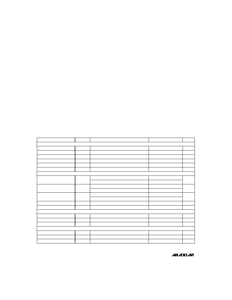
ABSOLUTE MAXIMUM RATINGS
ELECTRICAL CHARACTERISTICS
(V
DD
= +5V ±5%, REF+ = 5V, REF- = GND, Read Mode (MODE = GND), T
A
= T
MIN
to T
MAX
, unless otherwise noted.)
Stresses beyond those listed under "Absolute Maximum Ratings" may cause permanent damage to the device. These are stress ratings only, and functional
operation of the device at these or any other conditions beyond those indicated in the operational sections of the specifications is not implied. Exposure to
absolute maximum rating conditions for extended periods may affect device reliability.
V
DD
to GND ..............................................................-0.3V to +7V
Digital Input Voltage to GND ......................-0.3V to (V
DD
+ 0.3V)
Digital Output Voltage to GND ...................-0.3V to (V
DD
+ 0.3V)
REF+ to GND..............................................-0.3V to (V
DD
+ 0.3V)
REF- to GND...............................................-0.3V to (V
DD
+ 0.3V)
IN_ to GND .................................................-0.3V to (V
DD
+ 0.3V)
Continuous Power Dissipation (T
A
= +70∞C)
24-Pin Narrow Plastic DIP
(derate 13.33mW/∞C above +70∞C)....................................1.08W
24-Pin SSOP (derate 8.00mW/∞C above +70∞C)..............640mW
24-Pin Narrow CERDIP
(derate 12.50mW/∞C above +70∞C) .........................................1W
28-Pin Wide Plastic DIP
(derate 14.29mW/∞C above +70∞C)....................................1.14W
28-Pin SSOP (derate 9.52mW/∞C above +70∞C)..............762mW
28-Pin Wide CERDIP
(derate 16.67mW/∞C above +70∞C)....................................1.33W
Operating Temperature Ranges
MAX114/MAX118C_ _...........................................0∞C to +70∞C
MAX114/MAX118E_ _ ........................................-40∞C to +85∞C
MAX114/MAX118M_ _ .....................................-55∞C to +125∞C
Storage Temperature Range .............................-65∞C to +150∞C
Lead Temperature (soldering, 10sec) .............................+300∞C
V
IN
_
= 5Vp-p
MAX11_M, f
SAMPLE
= 740kHz, f
IN
_
= 195.7kHz
GND < V
IN
_
< V
DD
MAX11_C/E, f
SAMPLE
= 1MHz, f
IN
_
= 195.8kHz
No-missing-codes guaranteed
CONDITIONS
V
V
REF-
V
DD
REF+ Input Voltage Range
k
1
2
4
R
REF
Reference Resistance
pF
32
C
IN
_
Input Capacitance
µA
±3
I
IN
_
Input Leakage Current
V
V
REF-
V
REF+
V
IN
_
Input Voltage Range
V/µs
3.1
15
Input Slew Rate, Tracking
LSB
±1
TUE
Total Unadjusted Error
Bits
8
N
Resolution
MHz
1
Input Full-Power Bandwidth
dB
45
SINAD
Signal-to-Noise Plus
Distortion Ratio
45
LSB
±1
DNL
Differential Nonlinearity
LSB
±1
Zero-Code Error
LSB
±1
Full-Scale Error
LSB
±1/4
Channel-to-Channel Mismatch
UNITS
MIN
TYP
MAX
SYMBOL
PARAMETER
MAX11_M, f
SAMPLE
= 740kHz, f
IN
_
= 195.7kHz
MAX11_C/E, f
SAMPLE
= 1MHz, f
IN
_
= 195.8kHz
dB
-50
THD
Total Harmonic Distortion
-50
MAX11_M, f
SAMPLE
= 740kHz, f
IN
_
= 195.7kHz
MAX11_C/E, f
SAMPLE
= 1MHz, f
IN
_
= 195.8kHz
dB
50
SFDR
Spurious-Free Dynamic
Range
50
V
GND
V
REF+
REF- Input Voltage Range
ACCURACY
(Note 1)
DYNAMIC PERFORMANCE
ANALOG INPUT
REFERENCE INPUT

MAX114/MAX118
+5V, 1Msps, 4 & 8-Channel,
8-Bit ADCs with 1µA Power-Down
_______________________________________________________________________________________
3
ELECTRICAL CHARACTERISTICS (continued)
(V
DD
= +5V ±5%, REF+ = 5V, REF- = GND, Read Mode (MODE = GND), T
A
= T
MIN
to T
MAX
, unless otherwise noted.)
Note 2:
Guaranteed by design.
Note 3:
Power-down current increases if logic inputs are not driven to GND or V
DD
.
WR
CS, RD, PWRDN, A0, A1, A2
µA
±3
I
INH
D0≠D7, RDY
D0≠D7, RDY, digital outputs = 0V to V
DD
I
SOURCE
= 360µA,
INT, D0≠D7
RDY, I
SINK
= 2.6mA
MODE
MODE
I
SINK
= 1.6mA,
INT, D0≠D7
CS, WR, RD, PWRDN, A0, A1, A2
CS, WR, RD, PWRDN, MODE, A0, A1, A2
CS, WR, RD, PWRDN, MODE, A0, A1, A2
CONDITIONS
Input High Current
±1
pF
5
8
C
OUT
Three-State Capacitance
(Note 2)
µA
±3
I
LKG
Three-State Current
V
4
V
OH
Output High Voltage
V
0.4
V
OL
Output Low Voltage
0.4
pF
5
8
C
IN
Input Capacitance (Note 2)
µA
±1
I
INL
Input Low Current
50
200
V
3.5
V
INH
Input High Voltage
MODE
2.4
CS, WR, RD, PWRDN, A0, A1, A2
V
UNITS
MIN
TYP
MAX
SYMBOL
PARAMETER
1.5
V
INL
Input Low Voltage
0.8
8
15
V
4.75
5.25
V
DD
Supply Voltage
V
DD
= 4.75V to 5.25V, V
REF
= 4.75V
CS = RD = V
DD
,
PWRDN = 0V (Note 3)
LSB
±1/16
±1/4
PSR
Power-Supply Rejection
µA
1
10
Power-Down V
DD
Current
CS = RD = 0V,
PWRDN = V
DD
mA
8
20
I
DD
V
DD
Supply Current
MAX11_C
MAX11_E/M
LOGIC INPUTS
LOGIC OUTPUTS
POWER REQUIREMENTS

MAX114/MAX118
+5V, 1Msps, 4 & 8-Channel,
8-Bit ADCs with 1µA Power-Down
4
_______________________________________________________________________________________
TIMING CHARACTERISTICS
(V
DD
= +4.75V, T
A
= +25∞C, unless otherwise noted.) (Note 4)
C
L
= 50pF
C
L
= 50pF,
R
L
= 5.1k
to V
DD
C
L
= 100pF (Note 5)
t
RD
< t
INTL
,
(Note 5)
ns
50
80
t
INTH
RD to INT Delay
(RD Mode)
ns
t
CRD
+
50
t
ACC0
Data-Access Time
(RD Mode)
(Note 7)
(Note 6)
ns
160
t
ACQ
ns
70
t
RDY
CS to RDY Delay
ns
0
t
CSH
CS to RD, WR
Hold Time
ns
0
t
CSS
CS to RD, WR
Setup Time
Minimum Acquisition
Time
ns
60
ns
320
t
UP
Power-Up Time
ns
700
t
CRD
Conversion Time
(RD Mode)
ns
660
t
CWR
Conversion Time
(WR-RD Mode)
t
DH
Data Hold Time
85
t
CRD
+
65
185
85
0
0
70
370
875
90
t
CRD
+
75
260
100
0
0
80
520
975
T
A
= T
MIN
to T
MAX
100
75
35
610
Pipelined mode, C
L
= 50pF
C
L
= 50pF
185
t
RD
< t
INTL
, C
L
= 100pF
(Note 5)
235
t
RD
< t
INTL
,
determined by t
ACC1
t
RD
> t
INTL
, determined by
t
ACC2
60
205
0.35
ns
80
t
IHWR
WR to INT Delay
ns
65
t
READ2
RD Pulse Width
(WR-RD Mode)
Pipelined mode, C
L
= 100pF
ns
30
t
AH
ns
380
500
t
INTL
WR to INT Delay
ns
150
t
RI
RD to INT Delay
ns
185
t
ACC1
Data-Access Time
(WR-RD Mode)
Multiplexer Address
Hold Time
ns
45
ns
160
t
READ1
RD Pulse Width
(WR-RD Mode)
µs
0.25
t
RD
Delay Between
WR
and
RD Pulses
µs
0.25
10
t
WR
WR Pulse Width
t
ID
Data-Access Time
after
INT
0.28
10
120
85
40
700
220
275
70
240
0.45
0.4
10
110
t
RD
> t
INTL
, C
L
= 100pF
(Note 5)
ns
90
t
ACC2
Data-Access Time
(WR-RD Mode)
130
Note 4:
Input control signals are specified with t
r
= t
f
= 5ns, 10% to 90% of 5V, and timed from a voltage level of 1.6V.
Note 5:
See Figure 1 for load circuit. Parameter defined as the time required for the output to cross 0.8V or 2.4V.
Note 6:
See Figure 2 for load circuit. Parameter defined as the time required for the data lines to change 0.5V.
Note 7:
Also defined as the Minimum Address-Valid to Convert-Start Time.
MAX11_C/E
T
A
= +25∞C
ALL GRADES
CONDITIONS
MIN
MAX
MIN
MAX
UNITS
MIN
TYP
MAX
SYMBOL
PARAMETER
MAX11_M
C
L
= 20pF
C
L
= 100pF
685
865
1125

MAX114/MAX118
+5V, 1Msps, 4 & 8-Channel,
8-Bit ADCs with 1µA Power-Down
_______________________________________________________________________________________
5
1.5
0.6
-60
140
CONVERSION TIME
vs. AMBIENT TEMPERATURE
0.8
0.7
1.4
TEMPERATURE (∞C)
t
CRD
(NORMALIZED TO VALUE AT V
DD
= +5V, +25∞C)
20
1.1
1.0
0.9
-20
100
60
1.3
1.2
V
DD
= +4.75V
V
DD
= +5V
V
DD
= +5.25V
MAX114/118-01
8.0
6.0
1k
10k
100k
EFFECTIVE NUMBER OF BITS vs.
INPUT FREQUENCY (WR-RD MODE)
INPUT FREQUENCY (Hz)
EFFECTIVE NUMBER OF BITS
1M
7.5
7.0
6.5
MAX114/118-02
f
SAMPLE
= 1MHz
V
IN
= 4.96Vp-p
0
0
400
SIGNAL-TO-NOISE RATIO
-100
-80
-40
-20
FREQUENCY (kHz)
RATIO (dB)
300
-60
100
200
500
MAX114/118-04
SAMPLE
FREQUENCY = 1MHz
SNR = 48.2dB
V
DD
= 4.75V
INPUT FREQUENCY =
195.8ksps
V
IN
= 4.72Vp-p
50
0
100k
AVERAGE POWER CONSUMPTION
vs. SAMPLING RATE USING PWRDN
10
40
SAMPLING RATE (CONVERSIONS/SEC)
POWER DISSIPATION (mW)
1k
20
30
10k
1M
MAX114/118-03
5
6
0
75
100
150 175
250
TOTAL UNADJUSTED ERROR
vs. POWER-UP TIME
1
4
MAX114/118-06
POWER-UP TIME, t
UP
(ns)
TUE (LSB)
125
200
225
3
2
12
0
-60
SUPPLY CURRENT vs. TEMPERATURE
(EXCLUDING REFERENCE CURRENT)
2
4
6
8
10
MAX114/118-08
TEMPERATURE (∞C)
SUPPLY CURRENT (mA)
60
100
140
-20
20
__________________________________________Typical Operating Characteristics
(V
DD
= +5V, T
A
= +25∞C, unless otherwise noted.)