
DEVICES INCORPORATED
LT4420
Dual 32-Tap Transversal FIR Filter
Advance Information
LOGIC Devices Incorporated
1
Jan. 4, 2002 LDS.4420 C
Communications Products
165 MHz Max Data Rate
330 MHz Max Core Clock Rate
16-bit Data and Coefficients Paths
64-Tap FIR Filter, Cascadable for More Filter Taps
512 User-determined Coefficients Options Per Tap
Multiple Operating Modes: Dual Filter, Single Filter,
32-Bit Data or Coefficient, Double Rate, Auto
Decimate, Asymmetric Coefficient Set Expansion,
and Matrix Multiplication
24- or 48-bit Data Output with User-Defined
Rounding, Limiting, and Selecting
Supports up to 64 Interleaved Data Streams or a
Decimation Factor up to 64:1 for Increasing Filter
Taps
Interleaved Accumulator Capability Adds Increased
Flexibility When Interleaving
Built-in Cascade Ports Allow up to 16 Devices to be
Cascaded Without Any Additional Hardware.
Pre/Post-Modulator Stage with Built-in
User-programmable Direct Digital
Synthesizer (32-bit Accumulator)
Auto Decimation Mode Eliminates the Need
for External Coefficient, Transfer and
Accumulator Controllers
1K Word by 16-bit Capture Buffer. Supports
the Microcontroller in Calculating New
Coefficients in Adaptive Filtering
Microcontroller Interface
2.5 Volt Power Supply
272 BGA Package Ball Pitch 1.27mm
LVCMOS I/O Interface
5V Tolerant I/O
Performs 10 Billion Multiply Accumulates Per
Second
Industrial Temperature Available
The LT4420 is a 165 MHz Dual 16-bit 32-tap Digital Finite Impulse Response (FIR) Filter designed to meet
the filter requirements of tele/data communications and video imaging applications.
This device operates in eight different modes for various applications: Dual Filter, Single Filter, 32-Bit
Data, 32-Bit Coefficient, Double Rate, Auto Decimate, Asymmetric Coefficient Set Expansion, and Matrix
Multiplication.
Designed to take advantage of symmetric coefficient sets, the LT4420 can be configured as a single 64-tap
symmetric FIR filter or a 32-tap asymmetric FIR filter. A 4K-tap symmetric FIR filter may be realized with
a decimation factor of 64:1 utilizing the internal accumulator. When Asymmetric Coefficient Set Expansion
mode is used, a 2K-tap filter can be realized using a coefficient cycling technique; data rate is inversely
proportional to the number of taps. 32-Bit Data or 32-Bit Coefficient Mode will allow the use of either 32-bit
Data/16-bit Coefficients or 16-bit Data/32-bit Coefficients respectively. In addition, the core data rate can
be increased to 330MHz in Double Rate mode. In Auto Decimate mode, the device will self-configure for
the programmed decimation factor and automatically cycle through the pre-programmed coefficient sets;
interleaved Auto Decimation can also be realized.
Interleave/Decimation Registers (I/D Registers) allow up to 64 interleaved data streams to be fed directly
into the device and filtered without being separated externally.
The LT4420 contains on-chip memory to store 512 coefficient sets, 16 Round/Limit/Select Sets, and a
1K word Capture Buffer.
The Capture Buffer, used for calculating coefficient sets for adaptive filtering, allows the microcontroller to
access both input and output data streams without stopping the device.
A unique cascading structure allows for a cascade depth of sixteen devices. Unlimited cascading possible
with additional hardware.
The LT4420 also includes a user controlled Pre/Post-Modulator with a built in DDS and Sine/Cosine ROMs.
FEATURES
DESCRIPTION

DEVICES INCORPORATED
LT4420
Dual 32-Tap Transversal FIR Filter
Advance Information
LOGIC Devices Incorporated
2
Jan. 4, 2002 LDS.4420 C
Communications Products
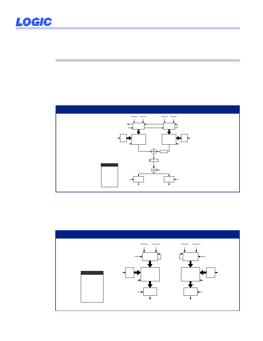
Figure 1. LT4420 Functional Block Diagram
"0
"
BZIF
Sixteen
COEFFICIENT
BANKS
(
5
1
2
s
e
t
s
x
1
6
-
b
i
t
s
/
b
a
n
k
)
DI
N
15-0
Sixteen
I/D
Register Cells
FILTER
A
(Sixteen
17 x 16-Bi
t
Multipliers
)
DAT
A
ALIG
N
AOUT
23-0
CASCADE
COMPENSATIO
N
DELAY
RL
S
CIRCUI
T
RL
S
CIRCUI
T
FILTER
B
(Sixteen
17 x 16-Bi
t
Multipliers
)
ASHEN
CL
K
ATXF
R
BTXF
R
BSHEN
INTERLEAVE
DECIMATION
CONTROL
FLAG LOGI
C
BUL
BOVF
AUL
AOVF
BL
L
AL
L
Sixteen
COEFFICIENT
BANKS
(
5
1
2
s
e
t
s
x
1
6
-
b
i
t
s
/
b
a
n
k
)
ACA
8-0
ACEN
9
BCA
8-0
BCEN
9
DAT
A
15-0
16
ADDR
14-0
15
R/
W
CS
Four
CAPTURE BUFFERs
(1K x 16-bit each)
DI
N
15-0
16
RI
N
15-0
16
AOUT
23-8
16
BI
O
23-8
16
CONFIGURATION/
CONTROL INTERFACE
RI
O
15-0
AACC
APASSA
APASSB
BACC
BPASSA
BPASSB
ARL
S
3-0
4
BRL
S
3-0
4
"0
"
AZIF
RI
N
15-0
CI
O
15-0
16
COE
16
16
24
AOE
BI
O
23
-
0
BOE
24
16
ROE
Modulator
(DDS)
Sixteen
I/D
Register Cells
Modulator
(DDS)
Modulator
(DDS)
Modulator
(DDS)
Resequencer
Resequencer
BSCAL
E
AFLT
BFLT
AMOD
BMOD
ASCAL
E

DEVICES INCORPORATED
LT4420
Dual 32-Tap Transversal FIR Filter
Advance Information
LOGIC Devices Incorporated
3
Jan. 4, 2002 LDS.4420 C
Communications Products
The LT4420 is a Dual 32-Tap Symmetric (16-Tap Asymmetric) Finite Impulse Response (FIR) Filter with
a Modulator Circuit that includes a Direct Digital Synthesizer (DDS). The filter core comprises Filter A
and Filter B. The two filter sides may be internally cascaded to create one 64-Tap Symmetric or one
32-Tap Asymmetric FIR Filter. There are two 16-bit data input ports (DIN15-0 and RIN15-0), two 16-bit I/O
ports (RIO15-0 and CIO15-0), one 24-bit I/O port (BIO23-0), and one dedicated output port (AOUT23-0).
Although the device is generally considered to be a 16-bit device (16-bit data/16-bit coefficient), the
ports may be combined for higher precision (see 32-Bit Data Mode, 32-Bit Coefficient Mode, and Double
Wide Output Mode in the Operating Modes section). All programming of the device is done through the
Configuration Registers via the 16-bit Configuration/Control Interface.
The LT4420 is made up of the following major functional blocks: Filter Cell, I/D Register Cell, Coefficient
Banks, Modulator, Round-Limit-Select Logic, Resequencer, and Microprocessor Control Interface. Other
functional blocks are discussed in the Functional Details section. Due to the high level of programmability,
the Functional Description discusses each functional block in detail.
A Filter Cell is essentially one 16 x 17-bit multiplier. There are sixteen Filter Cells in each filter side;
together there are thirty-two Filter Cells. Each Filter Cell calculates the product of a 17-bit data and a
16-bit coefficient; one 512 x 16-bit Coefficient Bank and two I/D Register Cells feed each Filter Cell (see
Figure 2).
ALU
A
B
ALU
A
B
1-64
1-64
1-64
1-64
DATA
REVERSAL
ALU
A
B
ALU
A
B
1-64
1-64
1-64
1-64
9
xCA
8-0
Coef0
Coef1
16
Coef511
Coef0
Coef1
16
Coef511
33
33
17
35
37
33
33
35
33
33
Coef0
Coef1
16
Coef511
Coef0
Coef1
16
Coef511
Reverse Data Out
Forward Data In
to Accumulator
16
16
16
Figure 2. Filter A/B
Functional Description

DEVICES INCORPORATED
LT4420
Dual 32-Tap Transversal FIR Filter
Advance Information
LOGIC Devices Incorporated
4
Jan. 4, 2002 LDS.4420 C
Communications Products
The I/D Register Cell makes possible various filtering techniques. Utilizing the internal ALU and feedback
path, the user may take advantage of symmetric coefficient sets thus doubling the number of taps (see
Figures 15 and 16). The 64-stage pipeline register per I/D Register Cell allows for interleaving up to 64
channels or decimating by a factor of 64.
One Coefficient Bank is provided for each multiplier; there are thirty-two Coefficient Banks total each storing
512 16-bit coefficients. Once the coefficients are loaded and stored, they are addressed through the
ACA
8-0
and BCA
8-0
address buses and can be changed on every cycle to support adaptive, interleaved,
multirate filtering. Coefficient Banks are double buffered and a full coefficient set is bank loaded after the
last coefficient of that set is loaded, thus supporting the ability to update a particular address while it is
in use. A set is considered to be 32 coefficients in Single Filter Mode or 16 coefficients in Dual Filter
Mode. Coefficients are loaded through the Configuration/Control Interface. The Output Circuitry allows for
numerous data routing and control options (see Figure 3).
Functional Description
AACC
A ACCM
"0"
46
46
BACC
46
B ACCM
"0"
BSCALE
ARLS
3-0
BRLS
3-0
4
4
ALIGN
24
BIO
23-0
BOE
from Filter A Core
46
CASCADE
COMPENSATING
DELAY
46
ROUND
LIMIT
SELECT
MODULATOR
ROUND
LIMIT
SELECT
MODULATOR
RESEQUENCER
AOUT
23-0
24
AOE
RESEQUENCER
from Filter B Core
47
AFLT
BFLT
AMOD
BMOD
24
ASCALE
Figure 3. Output Circuitry

DEVICES INCORPORATED
LT4420
Dual 32-Tap Transversal FIR Filter
Advance Information
LOGIC Devices Incorporated
5
Jan. 4, 2002 LDS.4420 C
Communications Products
The Modulator block may be used at either the input or output of the device. The pre- or post-modulators
(demodulators) can apply conventional amplitude modulation (AM), swept AM, phase modulation (PM),
quadrature AM, or frequency modulation (FM) to the data stream at a user-programmed carrier frequency.
They can also demodulate an incoming AM data stream and feed the results to the filter module for post
processing, such as baseband filtering. In conjunction with the filter module, the modulators also support
carrier frequency translation (heterodyning).
If greater input precision is desired, the user may configure the device to accept 32-bit data and 16-bit
coefficients (32-Bit Data Mode) or 32-bit coefficients and 16-bit data (32-Bit Coefficient Mode) while halving
the available number of filter taps. In addition, to compensate for the extra input precision, the output
precision may also be increased from 24 bits to 48 bits (Double Wide Output Mode).
Cascade ports (RIN15-0, RIO15-0, CIO15-0) facilitate the cascading of multiple devices. Access to the
Internal Summer through the BIO23-0 port and a Cascade Delay are provided for cascading up to 15
additional devices without the need for any extra hardware. Thus a 1,024-Tap Symmetric FIR can be
constructed and operated at full rate; a 65,536-Tap Symmetric FIR, when decimating by a factor of 64.
The I/D Register Cells feed the ALU inputs. They allow the device to facilitate interleaving up to 64 channels
and/or decimating by a factor of up to 64, in manual or operate in Auto-decimation Mode. There are 64
I/D Register Cells, thirty-two in the forward path and thirty-two in the reverse path. Each I/D Register Cell
contains a variable length delay of one through 64. This delay is automatically set and is based on the
interleave and decimation factors. Although the device is capable of handling 64 interleaved channels or a
decimation factor of up to 64, both cannot be implemented at the same time. The product of both must be
within 64, thus the limit is written as follows:
(Interleave Factor) x (Decimation Factor) < 64
i.e., (INTLV + 1) x (DECI + 1) < 64
For example, if one channel and no decimation are desired, the I/D Register Cell delay is automatically
set to one. If four channels and no decimation are desired, the I/D Register Cell delay is automatically
set to four. If eight channels and a decimation factor of eight are desired, the I/D Register Cell delay is
automatically set to 64.
Bits 8�13 of Configuration Register 47F3H and 47F4H are used to enter the number of desired channels to
be interleaved for Filter A and Filter B, respectively. If no interleaving is desired, bits 8-13 of the appropriate
Configuration Register must be set to 0. If two channels of interleaving are desired, bits 8-13 must be set to
1 and so on. A maximum of 64 channels may be interleaved.
Bits 0-5 of Configuration Register 47F3H and 47F4H are used to enter a decimation factor for Filter A and
Filter B respectively. If no decimation is desired, bits 0-5 of the appropriate Configuration Register must be
set to 0. If a decimation factor of two is desired, bits 0-5 of the appropriate Configuration Register must be
set to 1 and so on. The maximum decimation factor is 64.
Functional Description
I/D Register Cell

DEVICES INCORPORATED
LT4420
Dual 32-Tap Transversal FIR Filter
Advance Information
LOGIC Devices Incorporated
6
Jan. 4, 2002 LDS.4420 C
Communications Products
The ALUs are part of the I/D Register Cell and allow for doubling the number of taps when coefficients
of symmetry are used by pre-adding data values which are then multiplied by a common coefficient (see
Figure 5 and 6). The ALUs can perform the following operations: A+B, B-A, A+0, B+0. A+B is used
with even-symmetric coefficient sets. B-A is used with odd-symmetric coefficient sets. A+0 and B+0 are
used primarily when implementing interpolation. Bits 2-0 of Configuration Register 47F1H determine the
operation of the ALUs in Filter A. Bits 2-0 of Configuration Register 47F2H determine the operation of the
ALUs in Filter B. Thus, a 64-tap filter may be constructed with the thirty-two multipliers.
Functional Description
ALU
A
B
ALU
A
B
CENTER TAP COE
CENTER TAP - (N+1) COE
1-64
1-64
1-64
1-64
DAT
A
REVERSAL
ALU
A
B
ALU
A
B
CENTER TAP COE
CENTER TAP - (N+1) COE
1-64
1-64
1-64
1-64
DAT
A
REVERSAL
Delay Stage N�1
ALU
A
B
ALU
A
B
CENTER TAP - (N+1) COE
1-64
1-64
1-64
1-64
DAT
A
REVERSAL
EVEN-TAP MODE
ODD-TAP MODE
ODD-TAP INTERLEAVE MODE
2
CENTER TAP COE
2
Delay Stage N
N = DECIMATION FACTOR
1
2
3
4
5
6
7
8
Even-Tap, Even-Symmetric
Coefficient Set
Odd-Tap, Even-Symmetric
Coefficient Set
1
2
3
4
5
6
7
8
Even-Tap, Odd-Symmetric
Coefficient Set
1
2
3
4
5
6
7
Figure 5. Symmetric Coefficient Set Examples
Figure 6. I/D Register Data Paths
ALU

DEVICES INCORPORATED
LT4420
Dual 32-Tap Transversal FIR Filter
Advance Information
LOGIC Devices Incorporated
7
Jan. 4, 2002 LDS.4420 C
Communications Products
The Data Reversal blocks (see Figure 7) handle data resequencing for Data Reversal and Interleaved Data
Reversal, enabling the LT4420 to take advantage of symmetrical coefficients while decimating. The Data
Reversal block can also act as a simple delay RAM for Cascading, Single Filter Mode, and Asymmetric
Coefficient Set Expansion Mode. Data Reversal is enabled by bit 5 of Control Register 47F1H and bit 5 of
Control Register 47F2H for Filter A and Filter B respectively. When Auto-decimation is enabled, all the data
reversal control is handled by the LT4420 once the part is synchronized to the data stream by a falling
edge on xTXFR. When the user chooses to use manual decimation, xTXFR must be pulsed low every
((DECI + 1) x (INTLV + 1)) clock cycles and held low for INTLV + 1 clock cycles. When Data Reversal
is enabled, the functions of these blocks are two LIFOs for each interleaved data channel. While the
LIFO A for the current data channel is being filled, the LIFO B for that same channel is being read out.
The xTXFR signal in this case simply reverses the function of the two LIFOs every ((INT Factor) x (DEC
Factor)) clock cycles.
The coefficient banks store the coefficients, which feed into the multipliers in Filter A and Filter B. There
is a separate bank for each multiplier. Each bank can hold 512 16-bit coefficients. The banks are loaded
through the Configuration/Control Interface and normally directly addressed through the xCA address buses
except when in Auto-Decimation Mode. In Auto-decimation mode, the sequencing of the coefficients is
done automatically with the xCA address acting as a starting offset. Coefficient loading is discussed in the
Configuration/Control Interface section.
The Scale function should be used only in 32-bit Data Mode and 32-bit Coefficient Mode. In all other
modes, Scale should be disabled where it will not affect the data. When bit 3 of Configuration Register
47F0H is HIGH, Scale is enabled. When bit 3 of Configuration Register 47F0H is LOW, Scale is disabled.
The purpose of the Scale Circuitry is to properly scale Filter B's 46-bit data and combine it with Filter A's
46-bit data for a full scale 47-bit result. The Filter B 46-bit data is right shifted by twelve bit positions and
properly sign extended (BSCALE in block diagram) before being added to Filter A's 46-bit data, which is
left-shifted by four bits (ASCALE in block diagram). This shifting provides the proper relative binary weighting
of Filters A and B, while retaining enough format overhead to support 64-fold decimation.
When cascading, the Compensation Delay circuitry properly compensates for the extra delay created
when adding extra devices. This circuitry is a variable length delay which can add a delay of up to 64
to the pipeline, thus compensating for up to fifteen extra devices. When adding one extra device, the
compensating delay will be automatically set to a length of five. When adding two extra devices, the
compensating delay will automatically be set to a length of ten and so on. This is controlled by setting bits
8-11 of Configuration Register 47F0H; this setting will configure the Compensating Delay to properly adjust
to the position of the current LT4420 within the cascade chain.
Functional Description
Coefficient
Banks
Scale
Compensation
Delay
Figure 7. Data Reversal
Data Reversal
DEVICES INCORPORATED
LT4420
Dual 32-Tap Transversal FIR Filter
Advance Information
LOGIC Devices Incorporated
8
Jan. 4, 2002 LDS.4420 C
Communications Products
F
47
F
46
F
45
F
44
F
43
F
42
F
41
F
40
F
39
F
38
F
37
F
36
F
35
F
34
F
33
F
32
F
31
F
30
F
29
F
28
F
27
F
26
F
25
F
24
F
23
F
22
F
21
F
20
F
19
F
18
F
17
F
16
F
15
F
14
F
13
F
12
F
11
F
10
F
09
F
08
F
07
F
06
F
05
F
04
F
03
F
02
F
01
F
00
S
23
S
22
S
21
S
20
S
19
S
18
S
17
S
16
S
15
S
14
S
13
S
12
S
11
S
10
S
09
S
08
S
07
S
06
S
05
S
04
S
03
S
02
S
01
S
00
S
23
S
22
S
21
S
20
S
19
S
18
S
17
S
16
S
15
S
14
S
13
S
12
S
11
S
10
S
09
S
08
S
07
S
06
S
05
S
04
S
03
S
02
S
01
S
00
S
23
S
22
S
21
S
20
S
19
S
18
S
17
S
16
S
15
S
14
S
13
S
12
S
11
S
10
S
09
S
08
S
07
S
06
S
05
S
04
S
03
S
02
S
01
S
00
S
23
S
22
S
21
S
20
S
19
S
18
S
17
S
16
S
15
S
14
S
13
S
12
S
11
S
10
S
09
S
08
S
07
S
06
S
05
S
04
S
03
S
02
S
01
S
00
S
23
S
22
S
21
S
20
S
19
S
18
S
17
S
16
S
15
S
14
S
13
S
12
S
11
S
10
S
09
S
08
S
07
S
06
S
05
S
04
S
03
S
02
S
01
S
00
S
23
S
22
S
21
S
20
S
19
S
18
S
17
S
16
S
15
S
14
S
13
S
12
S
11
S
10
S
09
S
08
S
07
S
06
S
05
S
04
S
03
S
02
S
01
S
00
S
23
S
22
S
21
S
20
S
19
S
18
S
17
S
16
S
15
S
14
S
13
S
12
S
11
S
10
S
09
S
08
S
07
S
06
S
05
S
04
S
03
S
02
S
01
S
00
S
23
S
22
S
21
S
20
S
19
S
18
S
17
S
16
S
15
S
14
S
13
S
12
S
11
S
10
S
09
S
08
S
07
S
06
S
05
S
04
S
03
S
02
S
01
S
00
S
23
S
22
S
21
S
20
S
19
S
18
S
17
S
16
S
15
S
14
S
13
S
12
S
11
S
10
S
09
S
08
S
07
S
06
S
05
S
04
S
03
S
02
S
01
S
00
S
23
S
22
S
21
S
20
S
19
S
18
S
17
S
16
S
15
S
14
S
13
S
12
S
11
S
10
S
09
S
08
S
07
S
06
S
05
S
04
S
03
S
02
S
01
S
00
S
23
S
22
S
21
S
20
S
19
S
18
S
17
S
16
S
15
S
14
S
13
S
12
S
11
S
10
S
09
S
08
S
07
S
06
S
05
S
04
S
03
S
02
S
01
S
00
S
23
S
22
S
21
S
20
S
19
S
18
S
17
S
16
S
15
S
14
S
13
S
12
S
11
S
10
S
09
S
08
S
07
S
06
S
05
S
04
S
03
S
02
S
01
S
00
S
23
S
22
S
21
S
20
S
19
S
18
S
17
S
16
S
15
S
14
S
13
S
12
S
11
S
10
S
09
S
08
S
07
S
06
S
05
S
04
S
03
S
02
S
01
S
00
S
23
S
22
S
21
S
20
S
19
S
18
S
17
S
16
S
15
S
14
S
13
S
12
S
11
S
10
S
09
S
08
S
07
S
06
S
05
S
04
S
03
S
02
S
01
S
00
S
23
S
22
S
21
S
20
S
19
S
18
S
17
S
16
S
15
S
14
S
13
S
12
S
11
S
10
S
09
S
08
S
07
S
06
S
05
S
04
S
03
S
02
S
01
S
00
S
23
S
22
S
21
S
20
S
19
S
18
S
17
S
16
S
15
S
14
S
13
S
12
S
11
S
10
S
09
S
08
S
07
S
06
S
05
S
04
S
03
S
02
S
01
S
00
S
23
S
22
S
21
S
20
S
19
S
18
S
17
S
16
S
15
S
14
S
13
S
12
S
11
S
10
S
09
S
08
S
07
S
06
S
05
S
04
S
03
S
02
S
01
S
00
S
23
S
22
S
21
S
20
S
19
S
18
S
17
S
16
S
15
S
14
S
13
S
12
S
11
S
10
S
09
S
08
S
07
S
06
S
05
S
04
S
03
S
02
S
01
S
00
S
23
S
22
S
21
S
20
S
19
S
18
S
17
S
16
S
15
S
14
S
13
S
12
S
11
S
10
S
09
S
08
S
07
S
06
S
05
S
04
S
03
S
02
S
01
S
00
S
23
S
22
S
21
S
20
S
19
S
18
S
17
S
16
S
15
S
14
S
13
S
12
S
11
S
10
S
09
S
08
S
07
S
06
S
05
S
04
S
03
S
02
S
01
S
00
S
23
S
22
S
21
S
20
S
19
S
18
S
17
S
16
S
15
S
14
S
13
S
12
S
11
S
10
S
09
S
08
S
07
S
06
S
05
S
04
S
03
S
02
S
01
S
00
S
23
S
22
S
21
S
20
S
19
S
18
S
17
S
16
S
15
S
14
S
13
S
12
S
11
S
10
S
09
S
08
S
07
S
06
S
05
S
04
S
03
S
02
S
01
S
00
S
23
S
22
S
21
S
20
S
19
S
18
S
17
S
16
S
15
S
14
S
13
S
12
S
11
S
10
S
09
S
08
S
07
S
06
S
05
S
04
S
03
S
02
S
01
S
00
S
23
S
22
S
21
S
20
S
19
S
18
S
17
S
16
S
15
S
14
S
13
S
12
S
11
S
10
S
09
S
08
S
07
S
06
S
05
S
04
S
03
S
02
S
01
S
00
S
23
S
22
S
21
S
20
S
19
S
18
S
17
S
16
S
15
S
14
S
13
S
12
S
11
S
10
S
09
S
08
S
07
S
06
S
05
S
04
S
03
S
02
S
01
S
00
11000
10111
10110
10101
10100
10011
10010
10001
10000
01111
01110
01101
01100
01011
01010
01001
01000
00111
00110
00101
00100
00011
00010
00001
00000
SLCT
4-0
F
47
F
46
F
45
F
44
F
43
F
42
F
41
F
40
F
39
F
38
F
37
F
36
F
35
F
34
F
33
F
32
F
31
F
30
F
29
F
28
F
27
F
26
F
25
F
24
F
23
F
22
F
21
F
20
F
19
F
18
F
17
F
16
F
15
F
14
F
13
F
12
F
11
F
10
F
09
F
08
F
07
F
06
F
05
F
04
F
03
F
02
F
01
F
00
S
23
S
22
S
21
S
20
S
19
S
18
S
17
S
16
S
15
S
14
S
13
S
12
S
11
S
10
S
09
S
08
S
07
S
06
S
05
S
04
S
03
S
02
S
01
S
00
S
23
S
22
S
21
S
20
S
19
S
18
S
17
S
16
S
15
S
14
S
13
S
12
S
11
S
10
S
09
S
08
S
07
S
06
S
05
S
04
S
03
S
02
S
01
S
00
S
23
S
22
S
21
S
20
S
19
S
18
S
17
S
16
S
15
S
14
S
13
S
12
S
11
S
10
S
09
S
08
S
07
S
06
S
05
S
04
S
03
S
02
S
01
S
00
S
23
S
22
S
21
S
20
S
19
S
18
S
17
S
16
S
15
S
14
S
13
S
12
S
11
S
10
S
09
S
08
S
07
S
06
S
05
S
04
S
03
S
02
S
01
S
00
S
23
S
22
S
21
S
20
S
19
S
18
S
17
S
16
S
15
S
14
S
13
S
12
S
11
S
10
S
09
S
08
S
07
S
06
S
05
S
04
S
03
S
02
S
01
S
00
S
23
S
22
S
21
S
20
S
19
S
18
S
17
S
16
S
15
S
14
S
13
S
12
S
11
S
10
S
09
S
08
S
07
S
06
S
05
S
04
S
03
S
02
S
01
S
00
S
23
S
22
S
21
S
20
S
19
S
18
S
17
S
16
S
15
S
14
S
13
S
12
S
11
S
10
S
09
S
08
S
07
S
06
S
05
S
04
S
03
S
02
S
01
S
00
S
23
S
22
S
21
S
20
S
19
S
18
S
17
S
16
S
15
S
14
S
13
S
12
S
11
S
10
S
09
S
08
S
07
S
06
S
05
S
04
S
03
S
02
S
01
S
00
S
23
S
22
S
21
S
20
S
19
S
18
S
17
S
16
S
15
S
14
S
13
S
12
S
11
S
10
S
09
S
08
S
07
S
06
S
05
S
04
S
03
S
02
S
01
S
00
S
23
S
22
S
21
S
20
S
19
S
18
S
17
S
16
S
15
S
14
S
13
S
12
S
11
S
10
S
09
S
08
S
07
S
06
S
05
S
04
S
03
S
02
S
01
S
00
S
23
S
22
S
21
S
20
S
19
S
18
S
17
S
16
S
15
S
14
S
13
S
12
S
11
S
10
S
09
S
08
S
07
S
06
S
05
S
04
S
03
S
02
S
01
S
00
S
23
S
22
S
21
S
20
S
19
S
18
S
17
S
16
S
15
S
14
S
13
S
12
S
11
S
10
S
09
S
08
S
07
S
06
S
05
S
04
S
03
S
02
S
01
S
00
S
23
S
22
S
21
S
20
S
19
S
18
S
17
S
16
S
15
S
14
S
13
S
12
S
11
S
10
S
09
S
08
S
07
S
06
S
05
S
04
S
03
S
02
S
01
S
00
S
23
S
22
S
21
S
20
S
19
S
18
S
17
S
16
S
15
S
14
S
13
S
12
S
11
S
10
S
09
S
08
S
07
S
06
S
05
S
04
S
03
S
02
S
01
S
00
S
23
S
22
S
21
S
20
S
19
S
18
S
17
S
16
S
15
S
14
S
13
S
12
S
11
S
10
S
09
S
08
S
07
S
06
S
05
S
04
S
03
S
02
S
01
S
00
S
23
S
22
S
21
S
20
S
19
S
18
S
17
S
16
S
15
S
14
S
13
S
12
S
11
S
10
S
09
S
08
S
07
S
06
S
05
S
04
S
03
S
02
S
01
S
00
S
23
S
22
S
21
S
20
S
19
S
18
S
17
S
16
S
15
S
14
S
13
S
12
S
11
S
10
S
09
S
08
S
07
S
06
S
05
S
04
S
03
S
02
S
01
S
00
S
23
S
22
S
21
S
20
S
19
S
18
S
17
S
16
S
15
S
14
S
13
S
12
S
11
S
10
S
09
S
08
S
07
S
06
S
05
S
04
S
03
S
02
S
01
S
00
S
23
S
22
S
21
S
20
S
19
S
18
S
17
S
16
S
15
S
14
S
13
S
12
S
11
S
10
S
09
S
08
S
07
S
06
S
05
S
04
S
03
S
02
S
01
S
00
S
23
S
22
S
21
S
20
S
19
S
18
S
17
S
16
S
15
S
14
S
13
S
12
S
11
S
10
S
09
S
08
S
07
S
06
S
05
S
04
S
03
S
02
S
01
S
00
S
23
S
22
S
21
S
20
S
19
S
18
S
17
S
16
S
15
S
14
S
13
S
12
S
11
S
10
S
09
S
08
S
07
S
06
S
05
S
04
S
03
S
02
S
01
S
00
S
23
S
22
S
21
S
20
S
19
S
18
S
17
S
16
S
15
S
14
S
13
S
12
S
11
S
10
S
09
S
08
S
07
S
06
S
05
S
04
S
03
S
02
S
01
S
00
S
23
S
22
S
21
S
20
S
19
S
18
S
17
S
16
S
15
S
14
S
13
S
12
S
11
S
10
S
09
S
08
S
07
S
06
S
05
S
04
S
03
S
02
S
01
S
00
S
23
S
22
S
21
S
20
S
19
S
18
S
17
S
16
S
15
S
14
S
13
S
12
S
11
S
10
S
09
S
08
S
07
S
06
S
05
S
04
S
03
S
02
S
01
S
00
S
23
S
22
S
21
S
20
S
19
S
18
S
17
S
16
S
15
S
14
S
13
S
12
S
11
S
10
S
09
S
08
S
07
S
06
S
05
S
04
S
03
S
02
S
01
S
00
S
23
S
23
S
23
S
23
S
23
S
23
S
23
S
23
S
23
S
23
S
23
S
23
S
23
S
23
S
23
S
23
S
23
S
23
S
23
S
23
S
23
S
23
S
23
S
23
S
23
S
23
S
23
S
23
S
23
S
23
S
23
S
23
S
23
S
23
S
23
S
23
S
23
S
23
S
23
S
23
S
23
S
23
S
23
S
23
S
23
S
23
S
23
S
23
S
23
S
23
S
23
S
23
S
23
S
23
S
23
S
23
S
23
S
23
S
23
S
23
S
23
S
23
S
23
S
23
S
23
S
23
S
23
S
23
S
23
S
23
S
23
S
23
S
23
S
23
S
23
S
23
S
23
S
23
S
23
S
23
S
23
S
23
S
23
S
23
S
23
S
23
S
23
S
23
S
23
S
23
S
23
S
23
S
23
S
23
S
23
S
23
S
23
S
23
S
23
S
23
S
23
S
23
S
23
S
23
S
23
S
23
S
23
S
23
S
23
S
23
S
23
S
23
S
23
S
23
S
23
S
23
S
23
S
23
S
23
S
23
S
23
S
23
S
23
S
23
S
23
S
23
S
23
S
23
S
23
S
23
S
23
S
23
S
23
S
23
S
23
S
23
S
23
S
23
S
23
S
23
S
23
S
23
S
23
S
23
S
23
S
23
S
23
S
23
S
23
S
23
S
23
S
23
S
23
S
23
S
23
S
23
S
23
S
23
S
23
S
23
S
23
S
23
S
23
S
23
S
23
S
23
S
23
S
23
S
23
S
23
S
23
S
23
S
23
S
23
S
23
S
23
S
23
S
23
S
23
S
23
S
23
S
23
S
23
S
23
S
23
S
23
S
23
S
23
S
23
S
23
S
23
S
23
S
23
S
23
S
23
S
23
S
23
S
23
S
23
S
23
S
23
S
23
S
23
S
23
S
23
S
23
S
23
S
23
S
23
S
23
S
23
S
23
S
23
S
23
S
23
S
23
S
23
S
23
S
23
S
23
S
23
S
23
S
23
S
23
S
23
S
23
S
23
S
23
S
23
S
23
S
23
S
23
S
23
S
23
S
23
S
23
S
23
S
23
S
23
S
23
S
23
S
23
S
23
S
23
S
23
S
23
S
23
S
23
S
23
S
23
S
23
S
23
S
23
S
23
S
23
S
23
S
23
S
23
S
23
S
23
S
23
S
23
S
23
S
23
S
23
S
23
S
23
S
23
S
23
S
23
S
23
S
23
S
23
S
23
S
23
S
23
S
23
S
23
S
23
S
23
S
23
S
23
S
23
S
23
S
23
S
23
S
23
S
23
S
23
S
23
S
23
S
23
S
23
S
23
S
23
S
23
S
23
S
23
S
23
S
23
0
0
0
0
0
0
0
0
0
0
0
0
0
0
0
0
0
0
0
0
0
0
0
0
0
0
0
0
0
0
0
0
0
0
0
0
0
0
0
0
0
0
0
0
0
0
0
0
0
0
0
0
0
0
0
0
0
0
0
0
0
0
0
0
0
0
0
0
0
0
0
0
0
0
0
0
0
0
0
0
0
0
0
0
0
0
0
0
0
0
0
0
0
0
0
0
0
0
0
0
0
0
0
0
0
0
0
0
0
0
0
0
0
0
0
0
0
0
0
0
0
0
0
0
0
0
0
0
0
0
0
0
0
0
0
0
0
0
0
0
0
0
0
0
0
0
0
0
0
0
0
0
0
0
0
0
0
0
0
0
0
0
0
0
0
0
0
0
0
0
0
0
0
0
0
0
0
0
0
0
0
0
0
0
0
0
0
0
0
0
0
0
0
0
0
0
0
0
0
0
0
0
0
0
0
0
0
0
0
0
0
0
0
0
0
0
0
0
0
0
0
0
0
0
0
0
0
0
0
0
0
0
0
0
0
0
0
0
0
0
0
0
0
0
0
0
0
0
0
0
0
0
0
0
0
0
0
0
0
0
0
0
0
0
0
0
0
0
0
0
0
0
0
0
0
0
0
0
0
0
0
0
0
0
0
0
0
0
0
0
0
0
0
0
0
0
0
0
0
0
11000
10111
10110
10101
10100
10011
10010
10001
10000
01111
01110
01101
01100
01011
01010
01001
01000
00111
00110
00101
00100
00011
00010
00001
00000
SLCT
4-0
Table 1. Output Select Control
Table 2. Cascade Select Control

DEVICES INCORPORATED
LT4420
Dual 32-Tap Transversal FIR Filter
Advance Information
LOGIC Devices Incorporated
9
Jan. 4, 2002 LDS.4420 C
Communications Products
When cascading, the Align Circuitry is used to properly re-align the 24-bit BIO23-0 input back into the
48-bit filter sum. Filter B's Select Circuitry will no longer be used as discussed in the RLS discussion.
The selected 5-bit Select Register value will determine where the incoming 24-bit cascaded data will be
arranged within the 48-bit range inside the core (see Table 2). The MSB of the 24-bit word will be properly
sign extended to fill the 48-bit space. Anything smaller than the LSB of the 24-bit word will be zero filled
to fill the 48-bit space.
A Round/Limit/Select (RLS) Circuitry (see Figure 8) is provided on both AOUT23-0 and BIO23-0 ports
for programmable output control. Filter A RLS Circuitry is used for the overall filter in Single Filter Mode
operations. Both RLS Circuitry sections are programmable and can each store sixteen round values,
sixteen upper limit values, sixteen lower limit values, and sixteen select (windowing) schemes.
The registers are selected by RLS3-0, where a value of zero would pick the first register (register 0) in all
four sections (round, upper limit, lower limit, and select). Selecting of the registers is appropriately pipeline
delayed to match the data flowing through the output section. For instance, if RLS3-0 is set to a value of
three, round register two will be selected. On the next clock cycle, the sum of round register two and the
core data is then passed through the limit circuit where the value in upper limit register two and lower limit
register two are used for limiting. On the next cycle, the window scheme found in select register two would
then be used to select the appropriate 24 bits of data passed from the limit circuit.
The purpose of the Round Circuitry is to add a 48-bit round or offset value to the 47-bit data being passed
from the core. In the case of Dual Filter Mode operations, there are two separate cores. Sixteen separate
round or offset values can be stored in the sixteen registers. The value of the selected register will then be
added to the 47-bit core data. The sum is then sent to the Limit Circuitry. The round register values are
programmed into the round registers through the Configuration/Control Interface.
Round/Limit/
Select Circuitry
Functional Description
AR0
AR1
48
5
4
ARLS
3-0
RND
LIMIT
48
24
48
FILTER A RLS
DATA IN
47
DATA OUT
48
SELECT
AR15
AS0
AS1
AS15
AUL0
AUL1
AUL15
ALL0
ALL1
ALL15
48
BR0
BR1
48
5
4
BRLS
3-0
FILTER B RLS
48
RND
LIMIT
48
24
48
DATA IN
47
DATA OUT
SELECT
BR15
BS0
BS1
BS15
BUL0
BUL1
BUL15
BLL0
BLL1
BLL15
48
Figure 8. RSL Circuitry
Data Align

DEVICES INCORPORATED
LT4420
Dual 32-Tap Transversal FIR Filter
Advance Information
LOGIC Devices Incorporated
10
Jan. 4, 2002 LDS.4420 C
Communications Products
The purpose of the Limit Circuitry is to prevent the data from either going above or below a specified
range. Sixteen separate upper limit values can be stored in the sixteen upper limit registers. Sixteen
separate lower limit values can be stored in the sixteen lower limit registers. The upper limit value must
be greater than or equal to the lower limit value for the Limit Circuitry to work properly. If the 48-bit data
passed from the Round Circuitry is above the upper limit value, the upper limit value will then be passed
onto the Select Circuitry. If the 48-bit data passed from the Round Circuitry is below the lower limit value,
the lower limit value will then be passed onto the Select Circuitry. If the 48-bit data passed from the Round
Circuitry is within the specified limits, the value will remain untouched and passed onto the Select Circuitry.
The upper and lower limit values are programmed into the upper and lower limit registers through the
Configuration/Control Interface.
The purpose of the Select Circuitry is to pass 24 bits of the 48-bit core data either to the Modulator
or directly to the Resequencer (if the Modulator is bypassed). Any 24-bit window may be selected by
storing and selecting a 5-bit window code programmed into the select registers. The 5-bit window code
is programmed into the select registers through the Configuration/Control Interface. The window code
table is shown in Table 1.
When the selected data are passed from the filter to the modulator, only the 24 most significant bits will
be accepted into the 24 MSBS of the 32-bit phase accumulator. Only the 16 most significant bits will
be accepted by the mixer.
The Resequencer is used to implement various data multiplexing formats for the following:
� data alignment for interleaved decimation
� data alignment for interleaved interpolation
The Reseqencer blocks of the LT4420 re-interleaves interpolated samples and properly spaces interleaved
decimated samples at the output of the LT4420. This block is required only when either decimating
or interpolating interleaved signals. When interpolating the Resequencer can properly resequence 2
interleaved data channels with any integer interpolation factor up to and including 16. For example, lets
say you have 2 interleaved channels interpolated by 2, the normal filter output is as follows:
A1, A2, B1, B2, A3, A4, B3, B4
When RESEN=1, RESEQ=1, and DEPTH=1, for the reseqencer, this is properly resequenced as follows:
A1, B1, A2, B2, A3, B3, A4, B4
When decimating, the reseqencer can properly handle all valid integer interleave/decimation possibilities.
For example, lets say you have 3 interleaved channels decimated by a factor of 2, the filters accumulator
normally outputs data as follows:
A1, B1, C1, C1, C1, C1, A2, B2, C2, C2, C2, C2
where the first data channels comes out every clock cycle while the last data channel is held multiple clock
cycles. In this case, the reseqencer delays each data channel a total of a decimation factor clock cycles.
For this example, the output is as follows:
A1, A1, B1, B1, C1, C1, A2, A2, B2, B2, C2, C2
Round/Limit/
Select Circuitry
Cont'd
Functional Description
Resenquencer

DEVICES INCORPORATED
LT4420
Dual 32-Tap Transversal FIR Filter
Advance Information
LOGIC Devices Incorporated
11
Jan. 4, 2002 LDS.4420 C
Communications Products
A digital modulator circuit, comprising a direct digital synthesizer (DDS) and a multiplier-accumulator, can
be enabled at the input or output of each filter. The following modulation techniques may be implemented:
1. Amplitude Modulation (AM)
2. Swept AM
3. Phase Modulation (PM)
4. Quadrature Amplitude Modulation (QAM)
5. Frequency Modulation (FM)
Each of the LT4420's two modulator modules comprises two cascaded 32-bit phase accumulators, a 16-bit
sinusoidal lookup table, and a mixer (multiplier-accumulator). To effect different types of modulation,
the user can feed various incoming data or programmable constants into the two phase accumulators.
The user also may configure the chip to supply filtered data to the mixer as follows:
DIN -> filter -> modulate -> AOUT
or to post-filter the output of the mixer as follows:
DIN -> modulate -> filter -> AOUT
The upper phase accumulator loop is closed, (i.e., it generates a digitized sawtooth ramp), for conventional
fixed-frequency amplitude modulation (AM), swept-frequency AM (sAM), phase modulation (PM), and 16-,
256-, or other rate quadrature AM (xQAM). The user can periodically reset the accumulation to a known
value by asserting a synchronizing signal. It is open (i.e. it operates as a simple 2-input nonaccumulating
adder), for frequency modulation or compound AM/FM schemes. In sAM, FSC enters this loop to set the
sweep rate, whereas PHI0 + FSC determines the initial frequency of each sweep. In the other modes, FSC
sets carrier frequency and the sum of PHI0 + FSC determines the starting phase of this accumulation.
The lower phase accumulator loop is closed for FM and sAM and open in the other modes. The user can
force the accumulation to a known value by periodically asserting a synchronizing signal. In AM, it adds a
fixed, user-defined phase offset value or two alternating phase offsets. For PM and xQAM, the user can
introduce a filtered or unfiltered (via ports RIO15-0 and CIO15-0) phase modulation data stream here.
For AM, the top accumulator's output restarts at PHI0 + FSC with the arrival of each synchronizing pulse
and increments, modulo 32 bits, by FSC on each enabled data clock cycle. The lower accumulator adds
a constant (a 32-bit concatenation of OFFSET1 and OFFSET2) or two alternating constants (left-justified
OFFSET1 and OFFSET2) to this phase. The lookup table then converts this phase into a sampled
sinusoid. The modulating signal is applied directly to the mixer stage from the chip's main data path, either
before or after the filter, as required by the user. Typical application:
� moduating signal input: DIN
� modulated signal output: AOUT
� carrier frequency: FSC
� initial carrier phase: FSC + PHI0 + OFFSET
Functional Description
Modulator

DEVICES INCORPORATED
LT4420
Dual 32-Tap Transversal FIR Filter
Advance Information
LOGIC Devices Incorporated
12
Jan. 4, 2002 LDS.4420 C
Communications Products
Coherent AM demodulation is simple: bring in the modulated data stream, mix it with the carrier frequency
at the proper phase offset, and low-pass filter the output to remove the spurious (2 x FSC) component.
For noncoherent AM demodulation, one needs to mix the incoming signal with both the sine and cosine
of the carrier, as in the xQAM discussion below, then reconstruct magnitude and phase from the resulting
I and Q components.
For sAM, the top accumulator's output restarts at PHI0 + FSC with the arrival of each synchronizing pulse
and increments, modulo 32 bits, by FSC on each enabled data clock cycle. The lower accumulator also
accumulates, with an initial addend of OFFSET. Again, the modulating signal is applied directly to the
mixer only, either before or after filtering. Typical application:
� moduating signal input: DIN
� modulated signal output: AOUT
� initial carrier frequency: FSC + PHI0
� sweep rate: FSC (typically much smaller than PHI0)
� initial carrier phase: FSC + PHI0 + OFFSET
By programming the CHIRP value via the Configuration/Control Interface, the user can determine the
duration and repetition rate of the sweep.
To generate an xQAM signal with a simple rectangular constellation, the user configures the modulator for
conventional (not swept) AM, but with alternating sine and cosine, rather than steady sine, output from the
lookup table (TBL = 010 instead of 000). By sending I and Q components alternately down the data path,
the user causes the multiplier accumulator in the mixer to generate the following data stream:
I(n) x cos(n)
Q(n) x sin(n) + I(n) x cos(n)
I(n+1) x cos(n+1)
Q(n+1) x sin(n+1) + I(n+1) x cos(n+1)
I(n+2) x cos(n+2)
Q(n+2) x sin(n+2) + I(n+2) x cos(n+2)
In xQAM, the output data rate is one-half of the incoming data component rate. To accommodate twice the
data rate shown, the user can process the I and Q channels separately in the A and B portions of the chip,
and combine the results at the chip's output port.
To demodulate an xQAM signal, the user turns off the accumulation in the mixer and brings in a single
data stream instead of the separate I and Q components shown above. If both halves of the chip are
used to process a single data channel, one will generate I and the other will generate Q, both at the
incoming data rate.
In PM, the user closes the upper accumulator loop to generate the carrier and feeds a filtered or unfiltered
modulating data stream into the lower accumulator. In this application, the amplitude modulation input
into the mixer will generally be a constant or slowly-changing variable (e.g., automatic gain control). The
carrier frequency is dictated by FSC, the initial phase by FSC + PHI0. The modulating data will enter the
chip on DIN and can be filtered either preceding or following modulation. The user can set the constant
or slowly-changing, AGC-controlled amplitude over the RIO15-0 data cascade bus, which is used as an
input in this application.
Functional Description
Modulator Cont'd

DEVICES INCORPORATED
LT4420
Dual 32-Tap Transversal FIR Filter
Advance Information
LOGIC Devices Incorporated
13
Jan. 4, 2002 LDS.4420 C
Communications Products
In FM, the user brings a 32-bit wide modulating signal into RIO15-0 (MSBs) and CIO15-0 (LSBs). FSC,
which is added to this value, determines the center frequency. The upper accumulator acts as a simple
2-input adder, and the lower accumulator loop is closed. The constant or AGC-controlled amplitude is set
by DIN, which can also be varied for a combined AM/FM modulation scheme, if desired. The modulator
can also be programmed to serve as a static gain adjustment stage.
Functional Description
Modulator
Cont'd
Figure 9. Modulator

DEVICES INCORPORATED
LT4420
Dual 32-Tap Transversal FIR Filter
Advance Information
LOGIC Devices Incorporated
14
Jan. 4, 2002 LDS.4420 C
Communications Products
The user can cascade up to 16 devices without any additional hardware. This enables a group of sixteen
LT4420s to compute a single 1,024-Tap Symmetric FIR at full clock rate. If decimation is used, a
65,536-Tap FIR with a decimation of 64 is possible. When cascading, all devices must be in Single Filter
Mode. Cascading is implemented by chaining the LT4420's as follows (see Figure 10):
CIO15-0 of the first device should be connected to DIN15-0 of the next device, to complete the forward
data input path. RIN15-0 of the first device should be connected to RIO15-0 of the next device, to
complete the reverse data input path. BIO23-0 of the first device should be connected to AOUT23-0
of the next device, to combine the filter outputs of the devices. All additional devices are chained in
the same manner.
The last device in the cascade chain should have bit 0 of Configuration Register 47F0H set to 0, and
bits 11-8 of Configuration Register 47F0H set to 0. For all other devices in the cascade chain, bit 0 of
Configuration Register 47F0H must be set to 1. Bit 11-8 of Configuration Register 47F0H counts up as you
count back from the last device in the cascade chain.
Bits 11-8 of Configuration Register 47F0H compensate for the data path delay of the following devices in
the cascade chain. For each additional device in the cascade chain, the latency of the filter is increased
by 8 clock cycles.
For each stage, the partial result is limited to 24 bits. However the 24 bits passed between parts is first run
through the RLS circuitry, then re-aligned in the previous part through the align circuitry. The align circuitry
uses the Filter B select information to realign that result into the current 48 bit partial result. This allows for
very flexible bit growth control across multiple devices.
The LT4420 includes four capture buffers which can be used in calculating adaptive filtering coefficients
or to aid in debugging the root cause of overflow and limiting conditions. There are a total of four 256 x
16-bit memory buffers that collect data from the DIN15-0, RIN15-0, AOUT23-0 and BIO23-0 data paths.
According to their input source, these memories are separated into Filter A and Filter B capture RAM
and controlled individually in pairs with the corresponding configuration register. There are two operation
modes for these capture memories.
The first is Capture on Demand, used for adaptive filtering, where the memory starts to capture data when
a xSYNC signal is received and progresses until the memories are full.
Functional Description
Cascading
DIN
15-0
DOUT
23-0
I/D
REGISTERS
FILTER A
I/D
REGISTERS
FILTER B
CASCADE
COMPENSATION
DELAY
RLS
CIRCUIT
ATXFR
ASHEN
AACC
ARLS
3-0
COEF
BANK
COEF
BANK
ACA
RIO
15-0
BTXFR
BSHEN
BACC
BCA
CIO
15-0
RIN
15-0
BIO
23-0
BRLS
3-0
DATA
ALIGN
DIN
15-0
DOUT
23-0
I/D
REGISTERS
FILTER A
I/D
REGISTERS
FILTER B
RLS
CIRCUIT
ATXFR
ASHEN
AACC
ARLS
3-0
COEF
BANK
COEF
BANK
ACA
RIO
15-0
BTXFR
BSHEN
BACC
BCA
"0"
BSCALE
ASCALE
BSCALE
ASCALE
Figure 10. Cascade Mode-Two Devices
Capture Buffer

DEVICES INCORPORATED
LT4420
Dual 32-Tap Transversal FIR Filter
Advance Information
LOGIC Devices Incorporated
15
Jan. 4, 2002 LDS.4420 C
Communications Products
The second is Capture on-the-Fly, used in debugging where the memory starts to capture data once the
chip is initialized and progresses until one of the status flags (AOVF, BOVF, ALL, AUL, BLL, BUL) is set.
Even though the Capture on-the-Fly stops based on the setting of a flag, the address is realigned in this
mode, so that the earliest data before the halt condition occurred is in the capture buffer at offset zero.
Once the memory is full, a trigger condition occurs that can be monitored by the Configuration/Control
Interface. The memory can then be read if desired. When a memory is read by the Configuration/Control
Interface, it responds to the control bus, which provides the address with a read command. Output data
shall be available at the bus during the same CS cycle.
When either memory is full or a trigger condition occurs, the memory will stop writing data. It also
stores the current status of the overflow and limit flags into the status register for examination by the
Configuration/Control Interface.
The capture memory is always running if it is set to the Capture On-the-Fly Mode and the trigger condition
is never met. To save power, use the capture on demand mode, which exercises the memory only once.
In certain cases, the device can have overflow conditions that will trigger the overflow flags to indicate
that an overflow has occurred. There are six overflow flags pins on the part that will be triggered high
to indicate an overflow. The 46-bit accumulator in Filter A and Filter B can reach saturation, at which
point an overflow condition exists. The event will cause the AOVF or BOVF output flags to be set HIGH
two clock cycles after the overflow.
The AUL and BUL flags work similarly in that they both go HIGH two clock cycles after the data passing
through the limit circuitry is greater than the selected Upper Limit register value.
The ALL and BLL flags work similarly in that they both go HIGH two clock cycles after the data passing
through the limit circuitry is lower than the selected Lower Limit register value.
All flags are dynamically synchronous, thus when a flag is triggered active, it will remain HIGH for one
clock cycle.
Capture Buffer
Cont'd
Flag Logic
Functional Description
DEVICES INCORPORATED
LT4420
Dual 32-Tap Transversal FIR Filter
Advance Information
LOGIC Devices Incorporated
16
Jan. 4, 2002 LDS.4420 C
Communications Products
When bit 1 in Configuration Register 47F0H is set LOW, the device is in Single Filter Mode (see Figure 11)
where thirty-two independent multipliers are utilized to construct a 64-tap symmetrical FIR filter or a 32-tap
asymmetrical FIR filter. DIN15-0 is the data input for the filter and AFLT23-0 is the data output for the filter.
Cascade ports (RIN15-0, RIO15-0, CIO15-0) are provided to facilitate the cascading of multiple devices.
Access to the Internal Summer through the BIO24-0 port and a Cascade Delay are provided for cascading
up to 15 additional devices without the need for any extra hardware. Thus a 1,024-Tap Symmetric FIR can
be constructed and operated at full rate; 65,536-Tap Symmetric FIR when decimating by a factor of 64.
When bit 1 in Configuration Register 47F0H is set HIGH, the device is in Dual Filter Mode (see Figure 12),
in which two separate 32-tap symmetric FIRs or two separate 16-tap asymmetric FIRs can be constructed.
DIN15-0 is the data input and DOUT23-0 is the data output for Filter A. Either RIN15-0 or DIN15-0 can be
the data input for filter B, and BIO23-0 is the data output.
Operating Modes
Single Filter
Mode
Figure 11. Single Filter Mode
DIN
15-0
I/D
REGISTERS
FILTER A
I/D
REGISTERS
FILTER B
ATXFR
ASHEN
AACC
COEF
BANK
COEF
BANK
ACA
BTXFR
BSHEN
BACC
BCA
AFLT
23-0
RLS
CIRCUIT
ARLS
3-0
BLFT
23-0
RLS
CIRCUIT
BRLS
3-0
"0"
RIO
15-0
DFSUM
= 1
DBLWIDE = 0
MTX
= 0
FLTR
= 0
BSCALE
= 0
COESEL = x
FLTR
= 0
CASC
= 0
Control Settings
BSCALE
Dual Filter
Mode
Figure 12. Dual Filter Mode
DIN
15-0
I/D
REGISTERS
FILTER A
I/D
REGISTERS
FILTER B
ATXFR
ASHEN
AACC
COEF
BANK
COEF
BANK
ACA
8-0
BTXFR
BSHEN
BACC
BCA
8-0
AFLT
23-0
RLS
CIRCUIT
ARLS
3-0
BFLT
23-0
RLS
CIRCUIT
BRLS
3-0
RIN
15-0
DFSUM
= 0
DBLWIDE = 0
MTX
= 0
FLTR
= 0
BSCALE
= 0
COESEL = x
FLTR
= 1
CASC
= 0
LEGEND

DEVICES INCORPORATED
LT4420
Dual 32-Tap Transversal FIR Filter
Advance Information
LOGIC Devices Incorporated
17
Jan. 4, 2002 LDS.4420 C
Communications Products
When bit 6 in Configuration Register 47F0H is set HIGH, the device is in Auto-decimation Mode. Auto-
decimation works in either Single Filter Mode, dual filter mode, 32-Bit Data Mode, or 32-Bit Coefficient
Mode. In Single Filter Mode, the user should program filters A and B identically. When using Auto-
decimation, the device takes care of coefficient addressing and data routing for a given decimation factor.
ASHEN and BSHEN should be set LOW in this mode. A HIGH to LOW transition of ATXFR and BTXFR
should only be used once to synchronize the device with the start of valid data, after initially loading the
device with configuration/control data. Each additional falling ATXFR or BTXFR will resynchronize the part.
ACA
8-0
and BCA
8-0
will not function as a coefficient address during this mode but rather, it will provide the
starting coefficient addresses for the coefficient addressing sequence. For example, if four coefficient sets
are to be used and ACA
8-0
and BCA
8-0
are set to a value of 3, then coefficient sets 3, 4, 5, and 6 will be
automatically addressed and cycled through.
To determine the number of coefficient sets that will be used, the user must first determine the decimation
and interleave factor to be entered into Configuration Register 47F3H and 47F4H for Filter A and Filter
B respectively. The total number of coefficient sets to be used will thus be calculated by the following
equation:
(DECI + 1) x (INTLV + 1)
Please note, the DECI is the number entered into the device and is one less than the decimation factor. For
instance, if decimation by 2 is desired, the decimation factor is 2 and DECI is 1.
In the case of decimating 1 channel of data by a factor of 4, the total number of coefficient sets to be used
and automatically addressed is 4. In the case of decimating 4 channels of data by a factor of 4, the total
number of coefficient sets to be used and automatically addressed is 16.
Operating Modes
Auto-decimation
Mode

DEVICES INCORPORATED
LT4420
Dual 32-Tap Transversal FIR Filter
Advance Information
LOGIC Devices Incorporated
18
Jan. 4, 2002 LDS.4420 C
Communications Products
When bit 2 of Configuration Register 47F0H is LOW and the device is in Single Filter Mode and Scale is
enabled, the device is in 32-Bit Data Mode (see Figure 13). In this mode, the data width will be 32 bits and
the coefficients will be 16 bits, which the user must load identically into both filter channels. Although all
filter taps will be utilized and the reverse I/D Register Cell data path may be utilized for symmetric coefficient
sets, only half of the filter size may be realized. Thus, a 32-tap symmetric filter or a 16-tap asymmetric
filter may be constructed; Cascade Mode is not recommended during this operation, because the rounding
needed for the 24-bit interchip cascade ports may compromise arithmetic noise unacceptably.
The device will compensate for the extra data width internally thus utilizing the Scale Circuitry for proper
Filter A and Filter B summation (see Scale for further discussion). In this mode, DIN
15-0
is the most
significant 16 bit word and RIN
15-0
is the least significant 16 bit word. AOUT
23-0
will be used as the output
port. For extra output precision, enabling Double Wide Data Output Mode will concatenate output port
AOUT
23-0
and BIO
23-
0 for a 48-bit output.
Operating Modes
32-Bit Data Mode
Figure 13. 32-Bit Data Mode
DIN
15-0
AFLT
23-0
I/D
REGISTERS
FILTER A
I/D
REGISTERS
FILTER B
RLS
CIRCUIT
ATXFR
ASHEN
AACC
ARLS
3-0
COEF
BANK
COEF
BANK
ACA
8-0
BTXFR
BSHEN
BACC
BCA
8-0
RIN
15-0
BFLT
23-0
RLS
CIRCUIT
BRLS
3-0
"0"
DFSUM
= 1
DBLWIDE = 1
MTX
= 0
FLTR
= 1
BSCALE
= 1
COESEL = 0
FLTR
= 1
CASC
= 0
LEGEND
BSCALE
ASCALE

DEVICES INCORPORATED
LT4420
Dual 32-Tap Transversal FIR Filter
Advance Information
LOGIC Devices Incorporated
19
Jan. 4, 2002 LDS.4420 C
Communications Products
When bit 2 of Configuration Register 47F0H is HIGH and the device is in Single Filter Mode and Scale is
enabled, the device is in 32-Bit Coefficient Mode (see Figure 14). In this mode, the coefficients will be 32
bits and the data width will be 16 bits. Although all filter taps will be utilized and the reverse I/D Register
Cell data path may be utilized for symmetric coefficient sets, only half of the filter size may be realized.
Thus, a 32-tap symmetric filter or a 16-tap asymmetric filter may be constructed; Cascade Mode is not
recommended during this operation, because the rounding needed for the 24-bit interchip cascade ports
may compromise arithmetic noise unacceptably.
The device will compensate for the extra width internally thus utilizing the Scale Circuitry for proper Filter
A and Filter B summation (see Scale discussion). In this mode, Filter A Coefficient Bank stores the most
significant 16-bit word and Filter B Coefficient Bank stores the least significant 16-bit word. AOUT23-0
will be used as the output port. For extra output precision, enable Double Wide Data Output Mode to
concatenate AOUT23-0 and BIO23-0 output ports for a 48-bit output.
Operating Modes
Figure 14. 32-Bit Coefficient Mode
32-Bit Coefficient
Mode
DIN
15-0
AFLT
23-0
I/D
REGISTERS
FILTER A
I/D
REGISTERS
FILTER B
RLS
CIRCUIT
ATXFR
ASHEN
AACC
ARLS
3-0
COEF
BANK
COEF
BANK
ACA
BTXFR
BSHEN
BACC
BCA
BFLT
23-0
RLS
CIRCUIT
BRLS
3-0
"0"
DFSUM
= 1
DBLWIDE = 1
MTX
= 0
FLTR
= 1
BSCALE
= 1
COESEL = 1
FLTR
= 1
CASC
= 0
LEGEND
BSCALE
ASCALE

DEVICES INCORPORATED
LT4420
Dual 32-Tap Transversal FIR Filter
Advance Information
LOGIC Devices Incorporated
20
Jan. 4, 2002 LDS.4420 C
Communications Products
V
CC
INT
+2.5 V core voltage.
V
CC
O
+3.5 V I/O voltage. All pins must be connected.
CLK -- Master Clock
The rising edge of CLK strobes all enabled registers.
DIN
15-0
-- Data Input
DIN
15-0
is the 16-bit data input port to Filter A and is the primary data port for all modes. In Dual Filter
Mode, DIN
15-0
can also be the 16-bit input port to Filter B. Data is latched on the rising edge of clock. In
double rate mode, DIN
15-0
carries the first member of each pair of data samples entering the filter.
RIN
15-0
-- Reverse Data Input
In Dual Filter Mode, RIN
15-0
is the 16-bit data input port to Filter B. When cascading multiple devices in
Single Filter Mode, RIN
15-0
is connected to RIO
15-0
of the next LT4420 in the cascaded chain, to form the
reverse data path link. Data is latched on the rising edge of clock. In double rate mode, RIN
15-0
carries the
second member of each pair of data samples entering the filter.
AOUT
23-0
-- Filter A Data Output Port
AOUT
23-0
is the 24-bit registered data output port for the overall filter (Single Filter Mode) or
Filter A (Dual Filter Mode). In Double Wide Output Mode, AOUT
23-0
is the most significant 24
bits of the 48-bit output word.
DATA
15-0
-- Configuration/Control Data Bus
DATA
15-0
is the 16-bit bi-directional Configuration/Control Interface bus. When writing to the LT4420,
DATA
15-0
is latched on the rising edge of CS. When reading, the DATA
15-0
bus is driven a TDENA time
after the falling edge of CS.
BIO
23-0
-- Filter B Data I/O
In Dual Filter Mode, BIO
23-0
is the 24-bit registered data output port. In Single Filter Mode and when
cascading multiple devices it is the 24-bit registered Data Cascade port; BIO
23-0
is connected to AOUT
23-0
of the next LT4420 in the cascaded chain. In Double Wide Output Mode, BIO
23-0
is the least significant 24
bits of the 48-bit output word. In double rate operation, BIO
23-0
provides the second member of each pair of
data outputs, cotimed with the first member on
AOUT
23-0.f
CIO
15-0
-- Cascaded Forward Path Data I/O
In Single Filter Mode when cascading multiple devices, CIO
15-0
is the 16-bit registered cascade output port;
CIO
15-0
should be connected to DIN
15-0
of the next LT4420 of a cascaded chain. CIO
15-0
may also be
used as a modulation input whose function is defined by the modulator module configuration.
RIO
15-0
-- Cascaded Reverse Path Data I/O
In Single Filter Mode when cascading multiple devices, RIO
15-0
is the 16-bit reverse cascade data port;
RIO
15-0
is connected to RIN
15-0
of the previous LT4420 when used as the middle or last device of a
cascaded chain. RIO
15-0
may also be used as a modulation input whose function is selected by the
modulator configuration.
ADDR
14-0
-- Configuration/Control Address Bus
ADDR
14-0
is the 15-bit Configuration/Control Interface Address. ADDR
14-0
is latched by the falling edge
of CS. Setting ADDR
14
to 1 selects one of the control words, and only bits ADDR
10-0
are active, i.e.,
the chip ignores ADDR
13-11
.
Power
Signal Definitions
Clock
Inputs
Address
Outputs
Inputs/Outputs

DEVICES INCORPORATED
LT4420
Dual 32-Tap Transversal FIR Filter
Advance Information
LOGIC Devices Incorporated
21
Jan. 4, 2002 LDS.4420 C
Communications Products
ACA
8-0
-- Filter A Coefficient Address
ACA
8-0
determines which set of coefficients banks are fed to the filter cells. A value of 0 on ACA
8-0
selects
Coefficient Set 0. A value of 1 selects Coefficient Set 1 and so on. ACA
8-0
is latched into Coefficient Address
Register A on the rising edge of CLK when ACEN is LOW. During autodecimation operation, ACA
8-0
identifies the first of the sets of filter A coefficients which are to be used sequentially. Thus, if ACA
8-0
= N
at the beginning of the autodecimation sequence, the filter will use coefficient set N, then N+1, etc., until it
starts over again at the then-current of ACA
8-0.
BCA
8-0
-- Filter B Coefficient Address
BCA
8-0
determines which set of data in coefficient banks 16 through 31 is fed to the filter cells. A value of
0 on BCA
8-0
selects Coefficient Set 0. A value of 1 selects Coefficient Set 1 and so on. BCA
8-0
is latched
into Coefficient Address Register B on the rising edge of CLK when BCEN is LOW. During autodecimation
operation, BCA
8-0
identifies the first of the sets of filter A coefficients which are to be used sequentially.
Thus, if BCA
8-0
=N at the beginning of the autodecimation sequence, the filter will use coefficient set N, then
N+1, etc., until it starts over again at the then-current value of BCA
8-0
.
ARLS
3-0
-- Filter A Round/Limit/Select Control
ARLS
3-0
determines which of the sixteen user-programmable Round/Limit/Select (RLS) registers are used in
the Filter A RLS circuitry. A value of 0 on ARLS
3-0
selects Filter A RLS register 0. A value of 1 on ARLS
3-0
selects Filter RLS register 1 and so on. ARLS
3-0
is latched on the rising edge of CLK.
BRLS
3-0
-- Filter B Round/Limit/Select Control
BRLS
3-0
determines which of the sixteen user-programmable Round/Limit/Select (RLS) registers are used
in the Filter B RLS circuitry. A value of 0 on BRLS
3-0
selects Filter B RLS register 0. A value of 1 on
BRLS
3-0
selects Filter B RLS register 1 and so on. BRLS
3-0
is latched on the rising edge of CLK. During
cascade operation, BRLS
3-0
controls the "data align" module (see block diagram), which determines where
the 24 bits entering on BIO are to be added into the 48-bit internal data field.
R/W -- Read/Write Control
Reading or Writing to the internal registers is determined by R/W. To configure the interface for reading, R/W
must be HIGH when a falling edge of CS is detected. Within t
DDATA ns
, the contents of the addressed
register will be read out of the bi-directional DATA
15-0
port. To configure the device for writing, R/W must be
LOW when the falling edge of CS is detected. At that time, the addressed register will be stored and will be
written to (except for the Capture RAM) on the next rising edge of CS.
CS -- Chip Select
Reading or writing to the Configuration/Control registers through the DATA
15-0
port is enabled by CS. If no
reading or writing is desired, CS should be kept HIGH. R/W, ADDR
14-0
are latched on the falling edge of
CS. DATA
15-0
is latched on the next rising edge.
ACEN -- Filter A Coefficient Address Update Enable
When ACEN is LOW, data on ACA
8-0
is latched into Coefficient Address Register A on the rising edge
of CLK. When ACEN is HIGH, data on ACA
8-0
is not latched and the register's contents will not be
changed.
BCEN -- Filter B Coefficient Address Update Enable
When BCEN is LOW, data on BCA
8-0
is latched into Coefficient Address Register B on the rising edge
of CLK. When BCEN is HIGH, data on BCA
8-0
is not latched and the register's contents will not be
changed.
Address Cont'd
Signal Definitions
Controls

DEVICES INCORPORATED
LT4420
Dual 32-Tap Transversal FIR Filter
Advance Information
LOGIC Devices Incorporated
22
Jan. 4, 2002 LDS.4420 C
Communications Products
ASYNC -- A Sync
When not in Capture on the Fly Mode, ASYNC is used to start the Capture Buffer for Filter A.
BSYNC -- B Sync
When not in Capture on the Fly Mode, BSYNC is used to start the Capture Buffer for Filter B.
AMSYNC -- Filter A Modulator Sync
A falling AMSYNC is used to reset the DDS and accumulators in the Filter A modulator after a delay of
ASRD clock cycles. To ensure reproducible phase synchronization of modulator B, the user needs to apply
a falling edge to this pin after reprogramming any of the configuration registers, 47E0 through 47FF. The
chip reads AMSYNC at each rising edge of CLK.
BMSYNC -- Filter B Modulator Sync
A falling BMSYNC is used to reset the DDS and accumulators in the Filter B modulator after a delay of
BSRD clock cycles. To ensure reproducible phase synchronization of modulator B, the user needs to apply
a falling edge to this pin after reprogramming any of the configuration registers, 47E0 through 47FF. The
chip reads BMSYNC at each rising edge of CLK.
ARSYNC -- Filter A Resequencer Sync
When interpolating and interleaving, falling ARSYNC is used to properly arrange Filter A's core data so
that it arrives at the output properly interleaved. When interpolating interleaved data on channel A (or in
single-channel mode), the user needs to apply a falling edge to this pin after reprogramming any of the
configuration registers, 47E0 through 47FF. The chip reads ARSYNC at each rising edge of CLK.
BRSYNC -- Filter B Resequencer Sync
When interpolating and interleaving, falling BRSYNC is used to properly arrange Filter B's core data so
that it arrives at the output properly interleaved. When interpolating interleaved data on channel A (or in
single-channel mode), the user needs to apply a falling edge to this pin after reprogramming any of the
configuration registers, 47E0 through 47FF. The chip reads BRSYNC at each rising edge of CLK.
ATXFR -- Filter A Transfer
When in Manual Decimation Mode, ATXFR is used to change which LIFO in the data reversal circuitry
sends data to the reverse data path and which LIFO receives data from the forward data path in Filter A.
When ATXFR goes LOW, the LIFO sending data to the reverse data path becomes the LIFO receiving data
from the forward data path, and the LIFO receiving data from the forward data path becomes the LIFO
sending data to the reverse data path. The device must see a HIGH to LOW transition of ATXFR once every
((INTLV + 1) x (DECI+ 1)) clock cycles in order to switch Filter A's LIFOs for decimation.
When in Auto-decimation Mode, a HIGH to LOW transition of ATXFR is needed only once to synchronize
Filter A's LIFOs, coefficients, and accumulator with the incoming data stream. When in Matrix Multiplication
Mode, ATXFR is used to enable Filter A's ALU registers. To ensure proper timing of the filter's data reversal,
the user needs to apply a falling edge to ATXFR after reprogramming any of the configuration registers,
47E0 through 47FF. ATXFR is always latched on the rising edge of CLK.
Controls Cont'd
Signal Definition

DEVICES INCORPORATED
LT4420
Dual 32-Tap Transversal FIR Filter
Advance Information
LOGIC Devices Incorporated
23
Jan. 4, 2002 LDS.4420 C
Communications Products
BTXFR -- Filter B Transfer
When in Manual Decimation Mode, BTXFR is used to change which LIFO in the data reversal circuitry sends
data to the reverse data path and which LIFO receives data from the forward data path in Filter B. When
BTXFR goes LOW, the LIFO sending data to the reverse data path becomes the LIFO receiving data from the
forward data path, and the LIFO receiving data from the forward data path becomes the LIFO sending data to
the reverse data path. The device must see a HIGH to LOW transition of BTXFR once every ((INTLV + 1) x
(DECI + 1)) clock cycles in order to switch Filter B's LIFOs for decimation.
When in Auto-decimation Mode, a HIGH to LOW transition of BTXFR is needed only once to synchronize Filter
B's LIFOs, coefficients, and accumulator with the incoming data stream. When in Matrix Multiplication Mode,
BTXFR is used to enable Filter B's ALU registers. To ensure proper timing of the filter's data reversal, the user
needs to apply a falling edge to BTXFR after reprogramming any of the configuration registers, 47E0 through
47FF. BTXFR is always latched on the rising edge of CLK.
AACC -- Filter A Accumulate
When AACC is HIGH, Filter A Accumulator is enabled and the Filter A Accumulator Output Register is held.
When AACC is LOW, no accumulation is performed and the Filter A Accumulator Output Register is enabled
for loading. When AUTODECI (MODE control register, bit 6) is LOW, AAC is latched on each rising edge of
CLK. When AUTODECI is HIGH, AACC is ignored, and its function is handled automatically and internally.
BACC -- Filter B Accumulate
When BACC is HIGH, Filter B Accumulator is enabled for and the Filter B Accumulator Output Register is
held. When BACC is LOW, no accumulation is performed and the Filter B Accumulator Output Register is
enabled for loading. When AUTODECI (MODE control register, bit 6) is LOW, AACC is latched on each
rising edge of CLK. When AUTODECI is HIGH, AACC is ignored, and its function is handled automatically
and internally.
APASSA -- Filter A ALU Pass A
When bit 3 of Configuration Register 47F1H is HIGH, APASSA dynamically controls the Filter A ALUs. When
APASSA is HIGH, the forward data path for the Filter A ALU is enabled. When APASSA is LOW, the forward
data path for the Filter A ALU is forced to zero. When bit 3 of Configuration Register 47F1H is LOW, the
function of APASSA is controlled by 47F1, bit 1, and the pin should be tied to GND. APASSA is latched
on the rising edge of CLK.
APASSB -- Filter A ALU Pass B
When bit 3 of Configuration Register 47F1H is HIGH, APASSB dynamically controls the Filter A ALUs. When
APASSB is HIGH, the reverse data path for the Filter A ALU is enabled. When APASSB is LOW, the reverse
data path for the Filter A ALU is forced to zero. When bit 3 of Configuration Register 47F1H is LOW, the
function of APASSB is controlled by 47F1, bit 2, and the pin should be tied to GND. APASSB is latched
on the rising edge of CLK.
BPASSA -- Filter B ALU Pass A
When bit 3 of Configuration Register 47F2H is HIGH, BPASSA dynamically controls the Filter B ALUs. When
BPASSA is HIGH, the forward data path for the Filter B ALU is enabled. When BPASSA is LOW, the forward
data path for the Filter B ALU is forced to zero. When bit 3 of Configuration Register 47F2H is LOW, the
function of BPASSA is controlled by 47F2, bit 1, and the pin should be tied to GND. BPASSA is latched
on the rising edge of CLK.
Controls Cont'd
Signal Definition

DEVICES INCORPORATED
LT4420
Dual 32-Tap Transversal FIR Filter
Advance Information
LOGIC Devices Incorporated
24
Jan. 4, 2002 LDS.4420 C
Communications Products
BPASSB -- Filter B ALU Pass B
When bit 3 of Configuration Register 47F2H is HIGH, BPASSB dynamically controls the Filter B ALUs.
When BPASSB is HIGH, the reverse data path for the Filter B ALU is enabled. When BPASSB is LOW,
the reverse data path for the Filter B ALU is forced to zero. When bit 3 Configuration Register 47F2H is
LOW, the function of BPASSB is controlled by 47F2, bit 2, and the pin should be tied to GND. BPASSB
is latched on the rising edge of CLK.
AZIF -- Filter A Zero Insertion/Feedback
AZIF is used when interpolating or when in Asymmetric Coefficient Set Expansion mode. In all other
modes, AZIF must be tied LOW.
When interpolating and bit 12 of Configuration Register 47F0 is LOW, AZIF is used to force zeroe's on Filter
A's input for every N clock cycles (N = interpolation factor). When AZIF is HIGH, a zero is forced instead of
data. When AZIF is LOW, input data is passed to the filter.
When in Asymmetric Coefficient Set Expansion mode and bit 12 of Configuration Register 470H is HIGH,
AZIF must be toggled every N clock cycles to feed the old data back through the filter to achieve larger
asymmetrical filter sizes while sacrificing maximum input data rate (N = expansion factor). When AZIF is
HIGH, data is fed from the reverse data path back into the forward data path. When AZIF is LOW, input data
is passed to the filter. When bit 15 of Configuration register 47F0H is HIGH, AZIF becomes an enable for
the DIN register only. When AZIF is HIGH, the register is held, when AZIF is LOW, the register is enabled.
AZIF is latched on the rising edge of CLK.
BZIF -- Filter B Zero Insertion/Feedback
BZIF is used when interpolating or when in Asymmetric Coefficient Set Expansion mode. In
all other modes, BZIF must be tied LOW.
When interpolating and bit 13 of Configuration Register 47F0H is LOW, BZIF is used to force zero's on Filter
B's input for every N clock cycles (N = interpolation factor). When BZIF is HIGH, a zero is forced instead of
data. When BZIF is LOW, input data is passed to the filter.
When in Asymmetric Coefficient Set Expansion mode and bit 12 of Configuration Register 47F0H is HIGH,
BZIF must be toggled every N clock cycles to feed the old data back through the filter to achieve larger
asymmetrical filter sizes while sacrificing maximum input data rate (N = expansion factor). When BZIF is
HIGH, data is fed from the reverse data path back into the forward data path. When BZIF is LOW, input data
is passed to the filter. When bit 15 of Configuration Register 47F0H is HIGH, BZIF becomes an enable for
the RIN register only. When BZIF is HIGH, the register is held, when BZIF is LOW, the register is enabled.
BZIF is latched on the rising edge of CLK.
ASHEN -- Filter A Shift Enable
ASHEN is used in Asymmetric Coefficient Set Expansion Mode and when implementing polyphase filtering
techniques. ASHEN controls the shifting of data through the I/D registers and the enabled data ports; when
used, the interleaving and decimating factor should be set to 0. When ASHEN is LOW, data is latched
into the enabled data ports (Single Filter Mode - DIN23-0, RIN15-0, CIO15-0, RIO15-0; Dual Filter Mode -
DIN15-0, RIN15-0) and shifted through the I/D Registers on the rising edge of CLK. When ASHEN is HIGH,
data cannot be loaded into the enabled ports and data in the I/D Registers is held. In Single Filter Mode,
ASHEN and BSHEN should be connected together. ASHEN is latched on the rising edge of CLK.
Controls Cont'd
Signal Definition

DEVICES INCORPORATED
LT4420
Dual 32-Tap Transversal FIR Filter
Advance Information
LOGIC Devices Incorporated
25
Jan. 4, 2002 LDS.4420 C
Communications Products
BSHEN -- Filter B Shift Enable
BSHEN is used in Asymmetric Coefficient Set Expansion Mode and when implementing polyphase filtering
techniques. BSHEN controls the shifting of data through the I/D Registers and the enabled data ports; when
used, the interleaving and decimating factor should be set to 0. When BSHEN is LOW, data is latched
into the enabled data ports (Single Filter Mode - DIN23-0, RIN15-0, CIO15-0, RIO15-0; Dual Filter Mode -
DIN15-0, RIN15-0) and shifted through the I/D Registers on the rising edge of CLK. When BSHEN is HIGH,
data cannot be loaded into the enabled ports and data in the I/D Registers is held. In Single Filter Mode,
ASHEN and BSHEN should be connected together. BSHEN is latched on the rising edge of CLK.
AOE -- Filter A Output Enable
When AOE is LOW, AOUT23-0 is enabled for output. When AOE is HIGH, AOUT23-0 is placed in a
high-impedance state.
BOE -- Filter B Output Enable
When BOE is LOW, BIO23-0 is enabled for output. When BOE is HIGH, BIO23-0 is placed in a high-
impedance state and can be externally driven when cascading multiple devices.
COE -- CIO Output Enable
When COE is LOW, CIO15-0 is enabled for output. When COE is HIGH, CIO15-0 is placed in a high-
impedance state and can be externally driven when used in modulating.
ROE -- RIO Output Enable
When ROE is LOW, RIO15-0 is enabled for output. When ROE is HIGH, RIO15-0 is placed in a high-
impedance state and can be externally driven when used in modulating.
AOVF -- Filter A Overflow Flag
AOVF goes HIGH two clock cycles after the 46-bit Filter A Accumulator overflows.
BOVF -- Filter B Overflow Flag
BOVF goes HIGH two clock cycles after the 46-bit Filter B Accumulator overflows.
AUL -- Filter A Upper Limit Flag
AUL goes HIGH two clock cycles after the data passing through the Filter A Limit Circuitry is greater than
the selected Upper Limit register value.
BUL -- Filter B Upper Limit Flag
BUL goes HIGH two clock cycles after the data passing through the Filter B Limit Circuitry is greater than
the selected Upper Limit register value.
ALL --Filter A Lower Limit Flag
ALL goes HIGH two clock cycles after the data passing through the Filter A Limit Circuitry is less than the
selected Lower Limit register value.
BLL -- Filter B Lower Limit Flag
BLL goes HIGH two clock cycles after the data passing through the Filter B Limit Circuitry is less than the
selected Lower Limit register value.
Flags
Controls Cont'd
Signal Definition

DEVICES INCORPORATED
LT4420
Dual 32-Tap Transversal FIR Filter
Advance Information
LOGIC Devices Incorporated
26
Jan. 4, 2002 LDS.4420 C
Communications Products
Figure 15. Single/Dual Filter Data Mode Formats
15 14 13
2 1 0
�2
15
(Sign)
2
14
2
13
2
2
2
1
2
0
Filter A Data Input
15 14 13
2 1 0
�2
0
2
�1
2
�2
2
�13
2
�14
2
�15
Filter B Coefficient Input
15 14 13
2 1 0
�2
0
(Sign)
2
�1
2
�2
2
�13
2
�14
2
�15
Filter A Coefficient Input
45 44 43
2 1 0
�2
30
(Sign)
2
29
2
28
2
�13
2
�14
2
�15
45 44 43
2 1 0
�2
30
(Sign)
2
29
2
28
2
�13
2
�14
2
�15
Filter A Accumulator Output
Filter B Accumulator Output
15 14 13
2 1 0
�2
15
(Sign)
2
14
2
13
2
2
2
1
2
0
Filter B Data Input
47 44 43
2 1 0
�2
32
(Sign)
2
31
2
30
2
�13
2
�14
2
�15
Filter A Round Input
47 44 43
2 1 0
�2
32
(Sign)
2
31
2
30
2
�13
2
�14
2
�15
Filter B Round Input
Figure 16. 32-Bit Data Mode Formats
Figure 17. 32-Bit Coefficient Mode Formats
15 14 13
2 1 0
�2
31
(Sign)
2
30
2
29
2
28
2
17
2
16
15 14 13
2 1 0
2
15
2
14
2
13
2
2
2
1
2
0
Filter A Data Input (MSW)
Filter B Data Input (LSW)
15 14 13
2 1 0
�2
0
(Sign)
2
�1
2
�2
2
�13
2
�14
2
�15
Filter B Coefficient Input
15 14 13
2 1 0
�2
0
(Sign)
2
�1
2
�2
2
�13
2
�14
2
�15
Filter A Coefficient Input
45 44 43
2 1 0
�2
45
(Sign)
2
44
2
43
2
2
2
1
2
0
45 44 43
2 1 0
�2
30
(Sign)
2
29
2
28
2
�13
2
�14
2
�15
Filter A Accumulator Output
Filter B Accumulator Output
47 44 43
2 1 0
�2
44
(Sign)
2
43
2
42
2
�1
2
�2
2
�3
Filter A Round Input
15 14 13
2 1 0
�2
15
(Sign)
2
14
2
13
2
2
2
1
2
0
Filter A Data Input
15 14 13
2 1 0
2
�16
2
�17
2
�18
2
�29
2
�30
2
�31
Filter B Coefficient Input (LSW)
15 14 13
2 1 0
�2
0
(Sign)
2
�1
2
�2
2
�13
2
�14
2
�15
Filter A Coefficient Input (MSW)
45 44 43
2 1 0
�2
30
(Sign)
2
29
2
28
2
�13
2
�14
2
�15
45 44 43
2 1 0
�2
14
(Sign)
2
13
2
12
2
�29
2
�30
2
�31
Filter A Accumulator Output
Filter B Accumulator Output
15 14 13
2 1 0
�2
15
(Sign)
2
14
2
13
2
2
2
1
2
0
Filter B Data Input
47 44 43
2 1 0
�2
36
(Sign)
2
35
2
32
2
�09
2
�10
2
�11
Filter A Round Input
Data Formats

DEVICES INCORPORATED
LT4420
Dual 32-Tap Transversal FIR Filter
Advance Information
LOGIC Devices Incorporated
27
Jan. 4, 2002 LDS.4420 C
Communications Products
Control Register Map
ADDR (hex) Register Type Access
0000-3FFF Filter Coefficient Read/Write
4000-43FF Capture Buffers Read Only
4400-45FF Test Registers Read/Write
4600-46FF Round, Limit, Select Control Registers A Read/Write
4700-47FF Round, Limit, Select Control Registers B Read/Write
47E0-47FF Configuration Registers Read/Write (a)
4FE0-4FEF Rear Modulator Control Registers Read/Write
Table 3. Control/Coefficient Address Overview
(a)These need to be programmed first, immediately after power-up.
A14 13
12
11
10
9
8
7
6
5
4
3
2
1
A0
Table 4. Coefficient RAM Address Mapping
1 of 16 Filter
Taps
0 = Filter A
1 = Filter B
0 = Filters
1 = Other
Registers
Access to 512
Coefficient Sets
MSB
LSB
Example: 1F3F selects filter coefficient RAM, Filter A, and memory location 1F3 or location 499 of 512,
of filter tap F
Filter Select
Function Select
Filter Tap Select
Memory Select

DEVICES INCORPORATED
LT4420
Dual 32-Tap Transversal FIR Filter
Advance Information
LOGIC Devices Incorporated
28
Jan. 4, 2002 LDS.4420 C
Communications Products
Control Register Map
Address Range Mnemonic Captures: (b)
4000-40FF CAPD DIN
4100-41FF CAPA AOUT/DIN
4200-42FF CAPR RIN
4300-43FF CAPB BIO/RIN
Table 5. Capture Buffers
(b) The buffer captures the most recent 256 samples of its assigned data stream, starting a fresh
overwrite sequence when it has written to the highest value, number FF.
Table 6. Test Registers
ADDR (HEX) Mnemonic Register Number
4400-44FF TEST_ADDR Test_20
ADDR (HEX) Mnemonic Comments
4600 - 460F ARREG[15:0] A round; LSW
4610 - 461F ARREG[31:16] A round; mid
4620 - 462F ARREG[47:32] A round; MSW
4630 - 463F Reserved
4640 - 464F ALREG[15:0] A lower limit; LSW
4650 - 465F ALREG[31:16] A lower limit; mid
4660 - 466F ALREG[47:32] A lower limit; MSW
4670 - 467F Reserved
4680 - 468F AHREG[15:0] A upper limit; LSW
4690 - 469F AHREG[31:16] A upper limit; mid
46A0 - 46AF AHREG[47:32] A upper limit; MSW
46B0 - 46BF Reserved
46C0 - 46CF ASREG A select (shift)
46D0 - 46FF Reserved
4700 - 470F BRREG[15:0] B round; LSW
4710 - 471F BRREG[31:16] B round; mid
4720 - 472F BRREG[47:32] B round; MSW
4730 - 473F Reserved
4740 - 474F BLREG[15:0] B lower limit; LSW
4750 - 475F BLREG[31:16] B lower limit; mid
4760 - 476F BLREG[47:32] B lower limit; MSW
4770 - 477F Reserved
4780 - 478F BHREG[15:0] B upper limit; LSW
4790 - 479F BHREG[31:16] B upper limit; mid
47A0 - 47AF BHREG[47:32] B upper limit; MSW
47B0 - 47BF Reserved
47C0 - 47CF BSREG B select (shift)
47D0 - 47FF Reserved
Table 7. Round, Limit, Select Control (c)
(c) The user can preprogram 16 choices for each parameter.
Although the scale control registers are 16 bits wide, only the 5 LSBs of each are functional. Loading
a 16-bit binary value of xxxx_xxxx_xxx0_0000 will route the 24 LSBs of the 48-bit partial result to the
output bus, whereas xxxx_xxxx_xxx1_1000 will route the 24 MSBs. Select values exceeding binary
11000 = decimal 24 are reserved.

DEVICES INCORPORATED
LT4420
Dual 32-Tap Transversal FIR Filter
Advance Information
LOGIC Devices Incorporated
29
Jan. 4, 2002 LDS.4420 C
Communications Products
Control Register Map
ADDR (HEX) MNEMONIC Register Number
47E0 OFFSET_A2 Config. 10
47E1 OFFSET_A1 Config. 11
47E2 AFSC_LO Config. 12
47E3 AFSC_HI Config. 13
47E4 APHIO_LO Config. 14
47E5 APHIO_HI Config. 15
47E6 ACHIRP_LO Config. 16
47E7 ACHIRP_HI Config. 17
47E8 OFFSET_B2 Config. 18
47E9 OFFSET_B1 Config. 19
47EA BFSC_LO Config. 1A
47EB BFSC_HI Config. 1B
47EC BPHIO_LO Config. 1C
47ED BPHIO_HI Config. 1D
47EE BCHIRP_LO Config. 1E
47EF BCHIRP_HI Config. 1F
47F0 MODE Config. 0
47F1 CFGA Config. 1
47F2 CFGB Config. 2
47F3 LENA Config. 3
47F4 LENB Config. 4
47F5 RESEQ Config. 5
47F6 STATUS Config. 6
47F7 SPARE_1 Config. 7
47F8 CHIP_ID Config. 8
47F9 SPARE_2 Config. 9
47FA TEST_EN Config. A
47FB TEST_SITE Config. B
47FC ASRD Config. C
47FD BSRD Config. D
47FE DDSCTL Config. E
47FF SPARE_3 Config. F
4FE0 OFFSET_A2_R Config. 30
4FE1 OFFSET_A1_R Config. 31
4FE2 AFSC_LO_R Config. 32
4FE3 AFSC_HI_R Config. 33
4FE4 APHIO_LO_R Config. 34
4FE5 APHIO_HI_R Config. 35
4FE6 ACHIRP_LO_R Config. 36
4FE7 ACHIRP_HI_R Config. 27
4FE8 OFFSET_B2_R Config. 38
4FE9 OFFSET_B1_R Config. 39
4FEA BFSC_LO_R Config. 3A
4FEB BFSC_HI_R Config. 3B
4FEC BPHIO_LO_R Config. 3C
4FED BPHIO_HI_R Config. 3D
4FEE BCHIRP_LO_R Config. 3E
4FEF BCHIRP_HI_R Config. 3F
4FFC ASRD_R Config. 2C
$FFD BSRD_R Config. 2D
4FFE DDSCTL_R Config. 2E
Table 8. Configuration Register Summary

DEVICES INCORPORATED
LT4420
Dual 32-Tap Transversal FIR Filter
Advance Information
LOGIC Devices Incorporated
30
Jan. 4, 2002 LDS.4420 C
Communications Products
One resets any given module within the chip by loading its corresponding control register. The control
registers which effect resets are: 47F0-4, 47FC, 47FD, 47E1, 47E3, 47E5, and 47E7.
Table 9. Configuration Register Mode-Address 47F0H
BITS
FUNCTION
DESCRIPTION
0
Cascade
0: Single Device or Last in Cascade Series
CASC
1: First or Middle Device in Cascade Series
1
Dual Filter Mode
0: Single Filter Mode or 32-bit Mode
DFILT
1: Dual Filter Mode
2
32-bit Mode Select
0: 32-bit Data Mode
COE32
1: 32-bit Coefficient Mode
3
32-bit Mode Enable
0: 32-bit Mode Disabled
P32
1: 32-bit Mode Enabled
4
Matrix Multiplication Mode
0: Matrix Multiplication Mode Disabled
MTX
1: Matrix Multiplication Mode Enabled
5
Double Data Rate Mode
0: Double Data Rate Mode Disabled
DBLRATE
1: Double Data Rate Mode Enabled
6
Auto Decimation Mode
0: Auto Decimation Mode Disabled
AUTODCI
1: Auto Decimation Mode Enabled
7
Double Wide Output
0: 24 Bit Output Mode
DBLWIDE
1: 48 Bit Output Mode
11-8
Cascade Position
0000: Single or Last Device
CASPOS3-0
0001: Second to Last Device
0010: Third to Last Device
.
.
.
1110: Fourteenth to Last Device
1111: Fifteenth to Last Device
12
Filter A ZIF Function
0: AZIF Inserts Zeros
AFDBCK
1: AZIF Feedbacks Data for ASCE Mode
13
Filter B ZIF Function
0: BZIF Inserts Zeros
BFDBCK
1: BZIF Feedbacks Data for ASCE Mode
14
Dual Filter Mode Summation
0: Disable
DFSUM
1: DOUT= Filter A + Filter B
15
DIN/RIN Hold
0: Disable
HOLD
1: AZIF Holds DIN/BZIF Holds RIN
Mode Register
Address 47F0H
Control Register Map

DEVICES INCORPORATED
LT4420
Dual 32-Tap Transversal FIR Filter
Advance Information
LOGIC Devices Incorporated
31
Jan. 4, 2002 LDS.4420 C
Communications Products
Bit 0: CASC: Cascade:
When HIGH, the CASC bit signifies that this is the first or a middle device in a multi-device cascade chain.
This bit sets the reverse data path mux so that data comes from the RIN register instead of the forward
data path. When LOW, this bit signifies a single LT4420 device, or the last device in a cascade chain. This
bit may be set HIGH only when DFILT (47F0H bit 1), P32 (47F0H bit 3), DBLRATE (47F0H bit 5) and
DBLWIDE (47F0H bit 7) are all LOW.
Bit 1: DFILT: Dual Filter Mode:
When HIGH, the DFILT bit signifies that the LT4420 is acting as two independent 32 tap filters with a
common clock. When LOW, this bit signifies single filter mode (64 tap symmetrical), cascade mode (up
to 1024 tap symmetrical), or 32-bit mode (32-bit data or 32-bit coefficients at 32 tap symmetrical). This
bit may be set HIGH only when MODE (47F0H bit 0), P32 (47F0H bit 3) and DBLRATE (47F0H bit 5)
are all LOW. DBLWIDE (47F0H bit 7) may be HIGH only if DFSUM (47F0H bit 14) is also high, and the
Filter B output is not required.
Bit 2: COE32: 32-Bit Mode Select:
When HIGH the COE32 bit signifies that the device is in 32-bit coefficient mode if P32 (47F0H bit 3) is
HIGH. When LOW, this bit signifies that the device is in 32-bit data mode if P32 (47F0H bit 3) is high. This
bit may be set HIGH only when P32 (47F0H bit 3) is HIGH and CASC (47F0H bit 0), DFILT (47F0H bit 1),
and DBLRATE (47F0H bit 5) are all LOW.
Bit 3: P32: 32-Bit Precision Enable:
When HIGH, the P32 bit signifies that the LT4420 is in either 32-bit Data or 32-bit Coefficient mode
depending on the state of COE32 (47F0H bit 2). When LOW, this bit signifies that 32-bit mode is disabled.
P32 may be set HIGH only when CASC (47F0H bit 0), DFILT (47F0H bit 1) and DBLRATE (47F0H bit
5) are all LOW.
Bit 4: MTX: Matrix Multiplication Mode:
When HIGH, the MTX bit signifies that the LT4420 is in Matrix Multiplication Mode. This mode is valid in
Single, Dual, and 32-bit Modes of operation. Functionally, this bit redefines the function of XTXFR from Data
Reversal control, to ALU Enable. This allows the user to shift data into the ID registers, then bank-load the
data into the multipliers. The user then shifts through the set of coefficients while accumulating the results.
At the same time, the next set of data is shifted through the ID registers. When LOW, matrix multiplication
is disabled. MTX may be set HIGH only when DBLRATE (47F0H bit 5), AUTODECI (47F0H bit 6), ARVRS
(47F1H bit 5) and BRVRS (47F2H bit 5) are all LOW.
Bit 5: DBLRATE: Double Rate:
When HIGH, the DBLRATE bit signifies that the filter sections are running at twice the clock rate, but that the
modulator, RLS, resequencer, and capture RAM are not. The LT4420 is to take inputs from both the DIN
15-0
and the RIN
15-0
buses and multiplex them so that data can run through the core at twice the input/output
rate. The DIN
15-0
bus brings in the even samples, while the RIN
15-0
bus handles the odd samples. The output
is then de-multiplexed across the AOUT
23-0
and the BIO
23-0
busses, where the even samples appear on the
AOUT
23-0
bus and the odd samples appear on the BIO
23-0
bus. Because of the high-speed requirements,
DBLRATE is valid only in single filter mode, without Cascading, Asymmetrical Coefficient Set Expansion,
Matrix Multiplication or double precision. Since DBLRATE also uses both the AOUT
23-0
and the BIO
23-0
busses, Double Wide Output mode, and Resequencing are also invalid. When this bit is LOW, the core is
clocked at the same rate as the input. DBLRATE may be set HIGH only when CASC (47F0H bit 0), DFILT
(47F0H bit 1), P32 (47F0H bit 3), MTX (47F0H bit 4), DBLWIDE (47F0H bit 7), ARESEN (47F5H bit 5) and
BRESEN (47F5H bit 13) are all LOW.
Mode Register
Address 470H
Control Register Map

DEVICES INCORPORATED
LT4420
Dual 32-Tap Transversal FIR Filter
Advance Information
LOGIC Devices Incorporated
32
Jan. 4, 2002 LDS.4420 C
Communications Products
Bit 6: AUTODECI: Auto Decimation:
When HIGH, the AUTODECI bit signifies that the LT4420 controls all XTXFR, XCA, XACC, controls for FIR
filter with decimation, including interleaved decimation. When AUTODECI is active, it is active for BOTH
the A and B filters in Dual Filter Mode; however, AUTODECI will work with NO Decimation. AUTODECI
will not work with Asymmetrical Coefficient Set Expansion, Interpolation, Matrix Multiplication or Polyphase
filtering. This allows the user to send the LT4420 a single XTXFR pulse to initiate decimation, and all other
addressing is handled automatically. The coefficients must be loaded in a precise order, described in the
Auto Decimation section of the datasheet. When LOW, the AUTODECI bit signifies that the user will handle
all the LT4420 controls. AUTODECI may be set HIGH only when ARVRS (47F1H bit 5) and BRVRS (47F2H
bit 5) are HIGH and MTX (47F0 bit 4) is LOW.
Bit 7: DBLWIDE: Double Wide Output:
When HIGH, the DBLWIDE bit signifies that the LT4420 should split the output across both the AOUT
23-0
and the BIO
23-0
busses, giving a 48-bit result. Since the split occurs before the RLS circuitry, the ARLS
should select the 24 MSB's, while the BRLS should select the 24 LSB's of the 48-bit output word. When
LOW, the outputs are independent. DBLWIDE may be HIGH only when CASC (47F0H bit 0), P32 (47F0H
bit 3) and DBLRATE (47F0H bit 5) are all LOW. DBLWIDE is valid in Dual Filter Mode (DFILT 470H bit
1 is HIGH) only if DFSUM (47F0H bit 14) is also HIGH. The modulator should be used only at the filter
input in this mode.
Bits 11-8: CASPOS
3-0
: Cascade Position:
When CASPOS
3-0
is a non-zero value; it specifies the number of devices between this device and the end of
the cascade chain. This compensates the delay from one device to the next. For each additional device, the
DOUT
23-0
latency is increased by 4 clock cycles. CASCPOS
3-0
should have a non-zero value if only if CASC
(47F0H bit 0) is HIGH and DFILT (47F0H bit 1) is LOW.
Bit 12: AFDBCK: Filter A ZIF Function:
AFDBCK changes the function of the AZIF pin from Zero Insertion, used in Interpolation, to reverse path
feedback, (for Asymmetric Coefficient Set Expansion). When HIGH, AFDBCK causes a HIGH on AZIF to
feed the register delayed last stage of the Reverse ID path back into the beginning of the Forward ID path.
When used in conjunction with XSHEN, XPASSA, and XPASSB, this allows the LT4420 to accommodate
up to 2048 asymmetrical taps, at a proportionately reduced input data rate. When AFDBCK is LOW, the
AZIF pin will force a zero on the DIN input port, to facilitate interpolation. The function of this bit is
overridden by HOLD (47F0H bit 15). Although AFDBCK may be HIGH at any point, Asymmetric Coefficient
Set Expansion works only for non-interleaved and non-decimation modes. Matrix multiplication must also
be disabled.
Bit 13: BFDBCK: Filter B ZIF Function:
BFDBCK changes the function of BZIF pin from Zero Insertion, (used in Interpolation), to reverse path
feedback, (used in Asymmetric Coefficient Set Expansion). When HIGH, BFDBCK causes a HIGH on BZIF
to feed the register delayed last stage of the Reverse ID path back into the beginning of the Forward ID path.
When used in conjunction with XSHEN, XPASSA, and XPASSB, this allows the LT4420 to accommodate
up to 2048 asymmetrical taps, at a proportionately reduced input data rate. When BFDBCK is LOW,
the BZIF pin will force a zero on the RIN input port, to facilitate interpolation. The function of this bit is
overridden by HOLD (47F0H bit 15). Although BFDBCK may be HIGH at any point, Asymmetric Coefficient
Set Expansion works only for non-interleaved and non-decimation modes, without Matrix Multiplication or
Auto Decimation.
Bit 14: DFSUM: Dual Filter Summation:
DFSUM is used for quadrature (I,Q) modulation, where the I and Q channels are independently modulated
at the input of the LT4420 in Dual Filter Mode, then Filtered, then summed at the output and sent to the
transmitter via DOUT
23-0
. As the name states, Dual Filter Summation is valid only if DFILT (47F0H bit 1) is
HIGH. When DFSUM is LOW the A and B Filter outputs are independent, except in Single Filter mode.
Mode Register
Address 47F0H
Control Register Map

DEVICES INCORPORATED
LT4420
Dual 32-Tap Transversal FIR Filter
Advance Information
LOGIC Devices Incorporated
33
Jan. 4, 2002 LDS.4420 C
Communications Products
Bit 15: HOLD: DIN/RIN Hold:
This bit overrides the function of AFDBCK (47F0H Bit 12) and BFDBCK (47F0H bit 13), causing the AZIF
and BZIF pins to act as HOLD pins for the DIN
15-0
and RIN
15-0
input registers respectively. HOLD may not be
used in Asymmetric Coefficient Set Expansion.
BITS
FUNCTION
DESCRIPTION
0
ALU Mode
0: ALU Operation A+B
AALU
1: ALU Operation B-A
1
ALU Pass A
0: ALU Input A = 0
APASSA
1: ALU Input A = Forward Register Path
2
ALU Pass B
0: ALU Input B = 0
APASSB
1: ALU Input B = Reverse Register Path
3
ALU Pin Control
0: ALU Controled by Registers
APIN
1: ALU Controled by Pins
4
Tap Number
0: Even Number of Taps
ATAP
1: Odd Number of Taps
5
Data Reversal
0: Data Reversal Disabled
ARVRS
1: Data Reversal Enabled
6
Limit Enable
0: Limiting Disabled
ALMT
1: Limiting Enabled
8-7
Mixer Input
00: DIN15-0
AMIX1-0
01: Filter A Output
10: RIO15-0
11: CIO15-0
9
Reseqencer Source
0: Resequencer Input is Select Output
ARESSRC
1: Resequencer Input is Modulator Output
10
Modulator Downsampling
0: Down Sampling Disabled
ADWNSMPL
1: Down Sampling Enabled
11
On the Fly Recorder Enable
0: Capture Initiated by ASYNC
AFTREC
1: On the Fly Recorder Enabled
12
On the Fly Recorder Trigger
0: On the Fly Recorder Stopped by AOVF
AFTTRIG
1: On the Fly Recorder Stopped by AUL/ALL
13
Capture Buffer Enable
0: Filter A Capture Buffer Disabled
ARECEN
1: Filter A Capture Buffer Enabled
14
Input Offset Binary
0: Normal Operation (Two's Complement)
AOBIN
1: MSB of DIN15-0 Inverted
(Offset Binary Input Format)
15
Output Offset Binary
0: Normal Operation (Two's Complement)
AOBOUT
1: MSB of AOUT23-0 Inverted
(Offset Binary Output Format
Mode Register
Address 47F0H
Table 10. Configuration Register CFGA-Address 47F1H
CFGA Register
Address 47F1H
Control Register Map

DEVICES INCORPORATED
LT4420
Dual 32-Tap Transversal FIR Filter
Advance Information
LOGIC Devices Incorporated
34
Jan. 4, 2002 LDS.4420 C
Communications Products
Bit 0: AALU: Filter A ALU Mode:
When HIGH, the AALU bit tells filter A's ALUs to perform a B-A operation. This is used when odd symmetric
coefficients are required, such as in a Hilbert transform. When LOW, this bit tells Filter A's ALUs to perform
a A+B operation. This is used for even symmetric coefficients and all other modes of operation.
Bit 1: APASSA: Filter A ALU PASS A:
When HIGH, the APASSA bit tells filter A's ALUs to incorporate the forward data path into the filter result by
passing it to the A input of the ALU. When LOW, this bit signifies that the A input of the ALU will be forced
to zero, and the forward data path will be ignored for the calculation. Alternatively, if APIN (47F1H bit 3) is
HIGH, the user has dynamic control of this function via the APASSA control pin.
Bit 2: APASSB: Filter A ALU PASS B:
When HIGH, the APASSB bit tells filter A's ALUs to incorporate the reverse data path into the filter result by
passing it to the B input of the ALU. When LOW, this bit signifies that the B input of the ALU will be forced
to zero, and the reverse data path will be ignored for the calculation. Alternatively, if APIN (47F1H bit 3) is
HIGH, the user has dynamic control of this function via the APASSB control pin.
Bit 3: APIN: Filter A ALU Pin Control:
When HIGH, the APIN bit tells the LT4420 that the APASSA and APASSB functions are dynamically
controlled by the control pins of the same name. When LOW, this bit tells the LT4420 that the APASSA and
APASSB functions are statically controlled by control register 47F1H bits 1 and 2, respectively.
Bit 4: ATAP: Filter A Odd/Even Tap Control:
When HIGH, the ATAP bit configures filter A for an odd number of symmetrical taps. In this mode, the center
tap is duplicated on both the A and B inputs of the final multiplier of the filter. To correctly compensate for
this, the user must load the center tap divided by two. In an odd tap, odd symmetry filter, the center tap will
be zero. When ATAP is LOW, filter A is configured for an even number of taps when doing a symmetrical
filter, or an even or odd number of taps when doing Asymmetrical Coefficient Set Expansion.
Bit 5: ARVRS: Filter A Data Reversal Control:
When HIGH, the ARVRS bit configures filter A's lifos for data reversal, which is required for symmetrical
decimation. When LOW, ARVRS sets the data reversal block to function like a normal ID register delay. This
is required for Asymmetric Coefficient Set Expansion and all other non-decimation modes.
Bit 6: ALMT: Filter A Limit Enable:
When HIGH, ALMT enables filter A's limiting circuitry, allowing the user to saturate any result that is outside
the current selection window for AOUT
23-0
. When LOW, the filter A limiting circuitry is disabled.
Bit 8-7: AMIX
1-0
: Filter A Mixer Input:
AMIX
1-0
selects the data source for the multiplier in the modulator. When AMIX
1-0
= 00, the source is the
DIN
15-0
data bus. This is used in amplitude (AM), quadrature amplitude (QAM), or swept amplitude (sAM)
modulation or demodulation at the filter input. When AMIX
1-0
= 01, the source is Filter A's output. This is
used in AM and Swept AM at the filter output. When AMIX
1-0
= 10, the source is RIO
15-0
, which may be used
as a constant or variable gain in either frequency (FM) or phase (PM) modulation. When AMIX
1-0
= 11, the
source is CIO
15-0
, which also may be used as a constant or variable gain in either FM or PM.
Bit 9: ARESSRC:
Filter A Resequencer Source: When HIGH, ARESSRC sets filter A's resequencer's source to the modula-
tor's output. When LOW, the resequencer's source is set to the output of the rounding, limiting, scaling
(ARLS) circuitry.
CFGA Register
Address 47F1H
Control Register Map

DEVICES INCORPORATED
LT4420
Dual 32-Tap Transversal FIR Filter
Advance Information
LOGIC Devices Incorporated
35
Jan. 4, 2002 LDS.4420 C
Communications Products
Bit 10: ADWNSMPL: Filter A Modulator Down Sampling:
When HIGH, ADWNSMPL enables Filter A's modulator to down sample by either 2 or 4, based on the state
of ATBL
2-0
(47FEH bits 2-0). This is accomplished by accumulating the sin/cos samples selected by ATBL
2-0
(47FEH bits 2-0) into a single result. Applications include quadrature amplitude modulation, in which I and
Q samples will enter the modulator on alternate clock cycles. Please note: This is in the modulator only, and
is not related to decimation. When LOW, ADWNSMPL disables the accumulator in the modulator, so that
all samples appear at the modulator output.
Bit 11: AFTREC: Filter A On the Fly Recorder Enable:
When HIGH, AFLTREC changes the function of the A capture buffer from a user-triggered capture to a free-
running capture that halts on an error condition defined by AFTTRIG (47F1H bit 12). Used in debugging
this allows the user to examine both the input and the output leading up to the overflow or limit condition
occurring. When LOW, AFLTREC states that the A capture buffer is started based on the ASYNC control
pin, and will write until it is full. To enable the capture buffer for either of these modes, set ARECEN
(47F1H bit 13) HIGH.
Bit 12: AFTTRIG: Filter A On the Fly Recorder Trigger:
When HIGH, and with the capture buffer in flight recorder mode, filter A's capture buffer is halted by either
the assertion of AUL or ALL, caused by the ARLS circuitry hitting either the upper or lower limit. When
LOW, and with the capture buffer in flight recorder mode, filter A's capture buffer is halted by the assertion of
AOVF, caused by the A accumulator overflowing. To enable the capture buffer for flight recorder mode, set
ARECEN (47F1H bit 13) and AFTREC (47F1H Bit 11) HIGH.
Bit 13: ARECEN: Filter A Capture Buffer Enable:
When HIGH, ARECEN enables filter A's capture buffer for either capture buffer mode, or flight recorder
mode, dependent upon the state of AFTREC (47F1H bit 11). When LOW, filter A's capture buffer is
disabled.
Bit 14: AOBIN: Filter A Offset Binary Input:
When HIGH, the MSB of DIN
15-0
is inverted to convert from Offset Binary to Two's Complement numbering.
This is used to directly connect the input of the LT4420 to an ADC with a unipolar (unsigned or biased)
output format. When LOW, the MSB of DIN
15-0
is not inverted and is expected in Two's Complement format.
The internal data path of the LT4420 is always in two's complement format.
Bit 15: AOBOUT: Filter A Offset Binary Output:
When HIGH, the MSB of AOUT
23-0
is inverted to convert from Two's Complement to Offset Binary number-
ing. This is used to directly connect the output of the LT4420 to a DAC with a unipolar input format. When
LOW, the MSB of AOUT
23-0
is not inverted and is in Two's Complement format.
CFGA Register
Address 47F1H
Cont'd
Control Register Map

DEVICES INCORPORATED
LT4420
Dual 32-Tap Transversal FIR Filter
Advance Information
LOGIC Devices Incorporated
36
Jan. 4, 2002 LDS.4420 C
Communications Products
CFGB Register
Address 47F2H
BITS
FUNCTION
DESCRIPTION
0
ALU Mode
0: ALU Operation A+B
BALU
1: ALU Operation B-A
1
ALU Pass A
0: ALU Input A = 0
BPASSA
1: ALU Input A = Forward Register Path
2
ALU Pass B
0: ALU Input B = 0
BPASSB
1: ALU Input B = Reverse Register Path
3
ALU Pin Control
0: ALU Controled by Registers
BPIN
1: ALU Controled by Pins
4
Tap Number
0: Even Number of Taps
BTAP
1: Odd Number of Taps
5
Data Reversal
0: Data Reversal Disabled
BRVRS
1: Data Reversal Enabled
6
Limit Enable
0: Limiting Disabled
BLMT
1: Limiting Enabled
8-7
Mixer Input
00:
RIN15-0
BMIX1-0
01:
Filter B Output
10:
DIN15-0
11:
CIO15-0
9
Reseqencer Source
0: Resequencer Input is Select Output
BRESSRC
1: Resequencer Input is Modulator Output
10
Modulator Downsampling
0: Down Sampling Disabled
BDWNSMPL
1: Down Sampling Enabled
11
Flight Recorder Enable
0: Capture Initiated by BSYNC
BFTREC
1: Flight Recorder Enabled
12
Flight Recorder Trigger
0: Flight Recorder Stopped by BOVF
BFTTRIG
1: Flight Recorder Stopped by BUL/BLL
13
Capture Buffer Enable
0: Filter B Capture Buffer Disabled
BRECEN
1: Filter B Capture Buffer Enabled
14
Input Offset Binary
0: Normal Operation (Two's Complement)
BOBIN
1: MSB of RIN15-0 Inverted
(Offset Binary Input Format)
15
Output Offset Binary
0: Normal Operation (Two's Complement)
BOBOUT
1: MSB of BIO23-0 Inverted
(Offset Binary Output Format)
Table 11. Configuration Register CFGB-Address 47F2H
Control Register Map

DEVICES INCORPORATED
LT4420
Dual 32-Tap Transversal FIR Filter
Advance Information
LOGIC Devices Incorporated
37
Jan. 4, 2002 LDS.4420 C
Communications Products
Bit 0: BALU: Filter B ALU Mode:
When HIGH, the BALU bit tells filter B's ALUs to perform a B-A operation. This is used when odd symmetric
coefficients are required, such as in a Hilbert transform. When LOW, this bit tells Filter B's ALUs to perform
a A+B operation. This is used for even symmetric coefficients and all other modes of operation.
Bit 1: BPASSA: Filter B ALU PASS A:
When HIGH, the BPASSA bit tells filter B's ALUs to incorporate the forward data path into the filter result by
passing it to the A input of the ALU. When LOW, this bit signifies that the A input of the ALU will be forced
to zero, and the forward data path will be ignored for the calculation. Alternatively, if BPIN (47F2H bit 3) is
HIGH, the user has dynamic control of this function via the BPASSA control pin.
Bit 2: BPASSB: Filter B ALU PASS B:
When HIGH, the BPASSB bit tells filter B's ALUs to incorporate the reverse data path into the filter result by
passing it to the B input of the ALU. When LOW, this bit signifies that the B input of the ALU will be forced
to zero, and the reverse data path will be ignored for the calculation. Alternatively, if BPIN (47F2H bit 3) is
HIGH, the user has dynamic control of this function via the BPASSB control pin.
Bit 3: BPIN: Filter B ALU Pin Control:
When HIGH, the BPIN bit tells the LT4420 that the BPASSA and BPASSB functions are dynamically
controlled by the control pins of the same name. When LOW, this bit tells the LT4420 that the BPASSA and
BPASSB functions are statically controlled by control register 47F2H bits 1 and 2, respectively.
Bit 4: BTAP: Filter B Odd/Even Tap Control:
When HIGH, the BTAP bit configures filter B for an odd number of symmetrical taps. In this mode,
the center tap is duplicated on both the A and B inputs of the final multiplier of the filter. To correctly
compensate for this, the user must load the center tap divided by two. In an odd tap, odd symmetry
filter, the center tap will be zero. When BTAP is LOW, filter B is configured for an even number of taps
when doing a symmetrical filter, or an even or odd number of taps when doing Asymmetrical Coefficient
Set Expansion.
Bit 5: BRVRS: Filter B Data Reversal Control:
When HIGH, the BRVRS bit configures filter B's lifos for data reversal which is required for symmetrical
decimation. When LOW, BRVRS sets the data reversal block to function like a normal ID register delay. This
is required for Asymmetric Coefficient Set Expansion, and all other non-decimation modes.
Bit 6: BLMT: Filter B Limit Enable:
When HIGH, BLMT enables filter B's limiting circuitry, allowing the user to saturate any result that is outside
the current selection window for BIO
23-0
. When LOW, the filter B limiting circuitry is disabled.
Bit 8-7: BMIX
1-0
: Filter B Mixer Input:
BMIX
1-0
selects the data source for the multiplier in the modulator. When BMIX
1-0
= 00, the source is the
RIN
15-0
data bus. This is used in amplitude (AM), quadrature amplitude (QAM) or swept amplitude (sAM)
at the filter input. When BMIX
1-0
= 01, the source is Filter B's output. This is used in AM and sAM at the
output. When BMIX
1-0
= 10, the source is DIN
15-0
. This may also be used in AM, QAM or sAM at the
input. When BMIX
1-0
= 11, the source is CIO
15-0
which may be used as a constant or variable gain in either
frequency (FM) or phase (PM) modulation.
Bit 9: BRESSRC: Filter B Resequencer Source:
When HIGH, BRESSRC sets filter B's resequencer's source to the modulator's output. When LOW, the
resequencer's source is set to the output of the rounding, limiting, scaling (BRLS) circuitry.
CFGB Register
Address 47F2H
Control Register Map

DEVICES INCORPORATED
LT4420
Dual 32-Tap Transversal FIR Filter
Advance Information
LOGIC Devices Incorporated
38
Jan. 4, 2002 LDS.4420 C
Communications Products
Bit 10: BDWNSMPL: Filter B Modulator Down Sampling:
When HIGH, BDWNSMPL enables Filter B's modulator to down sample by either 2 or 4, based on the
state of BTBL
2-0
(47FEH bits 10-8). This is accomplished by accumulating the sin/cos samples selected
by BTBL
2-0
(47FEH bits 10-8) into a single result. Applications include quadrature amplitude modulation,
in which I and Q samples will enter the modulator on alternate clock cycles. Please note: This is in the
modulator only, and is not related to decimation. When LOW, BDWNSMPL disables the accumulator in the
modulator, so that all samples appear at the modulator output.
Bit 11: BFTREC: Filter B On the Fly Recorder Enable:
When HIGH, BFLTREC changes the function of the B capture buffer from a user-triggered capture, to
a free-running capture that halts on an error condition defined by BFTTRIG (47F2H bit 12). Used in
debugging this allows the user to examine both the input and the output leading up to the overflow or
limit condition occurring. When LOW, BFLTREC states that the B capture buffer is started based on the
BSYNC control pin, and will write until it is full. To enable the capture buffer for either of these modes,
set BRECEN (47F2H bit 13) HIGH.
Bit 12: BFTTRIG: Filter B On the Fly Recorder Trigger:
When HIGH, and with the capture buffer in flight recorder mode, filter B's capture buffer is halted by either
the assertion of BUL or BLL, caused by the BRLS circuitry hitting either the upper or lower limit. When
LOW, and with the capture buffer in flight recorder mode, filter B's capture buffer is halted by the assertion of
BOVF, caused by the B accumulator overflowing. To enable the capture buffer for flight recorder mode, set
BRECEN (47F2H bit 13) and BFTREC (47F2H Bit 11) HIGH.
Bit 13: BRECEN: Filter B Capture Buffer Enable:
When HIGH, BRECEN enables filter B's capture buffer for either capture buffer mode, or flight recorder
mode, dependant upon the state of BFTREC (47F2H bit 11). When LOW, filter B's capture buffer is
disabled.
Bit 14: BOBIN: Filter B Offset Binary Input:
When HIGH, the MSB of RIN
15-0
is inverted to convert from Offset Binary to Two's Compliment numbering.
This is used to directly connect the input of the LT4420 to an ADC with a unipolar (unsigned or biased)
output format. When LOW, the MSB of RIN
15-0
is not inverted and is expected in Two's Compliment format.
The internal data path of the LT4420 is always in two's compliment format.
Bit 15: BOBOUT: Filter B Offset Binary Output:
When HIGH, the MSB of BIO
23-0
is inverted to convert from Two's Compliment to Offset Binary numbering.
This is used to directly connect the output of the LT4420 to a DAC with a unipolar input format. When LOW,
the MSB of BIO
23-0
is not inverted and is in Two's Compliment format.
CFGB Register
Address 47F2H
Cont'd
Control Register Map

DEVICES INCORPORATED
LT4420
Dual 32-Tap Transversal FIR Filter
Advance Information
LOGIC Devices Incorporated
39
Jan. 4, 2002 LDS.4420 C
Communications Products
Bits 5-0: ADECI
5-0
: Filter A Decimation Factor:
When decimating, ADECI
5-0
+1 equals the decimation factor of 2-64; ADECI
5-0
= 0 implies a decimation
factor of unity, i.e., no decimation. When in Asymmetrical Coefficient Set Expansion (ASCE) ADECI
5-0
becomes the expansion factor, where (ADECI
5-0
+ 1)*2 equals the total possible expansion factor, at the
requirement of a reduced input rate of 1/((ADECI
5-0
+1)*2). Interleaving with ASCE is not possible. When
interleaving and decimating, truncating the result of (64/(ADECI
5-0
+1)) gives the maximum number of
interleaved channels decimated by ADECI
5-0
+1.
Bits 7-6: RESERVED:
All Reserved bits must be set to LOW.
Bits 13-8: AINTLV
5-0
: Filter A Interleave Factor:
AINTLV
5-0
+1 sets the number of interleaved data channels for filter A. When not decimating, the maximum
number of interleaved channels supported by the LT4420 is 64. When interleaving and decimating, truncat-
ing the result of (64/AINTLV
5-0
+1)) gives the maximum decimation possible for AINTLV
5-0
+1 interleaved data
channels. When interleaving and decimating, all interleaved channels must be decimated by the same
factor. When in ASCE, interleaving is not valid, and AINTLV
5-0
must be set to zero.
Bits 15-14: RESERVED:
All Reserved bits must be set to LOW.
Note: Although decimation and interleave factors up to 64 are valid, the maximum valid combination of interleave and decimation
is determined by (ADECI+1) x (AINTLV+1) <= 64
LENA Register
Address 47F3H
Table 12. Configuration Register LENA-Address 47F3H
BITS
FUNCTION
DESCRIPTION
5-0
Filter A Decimation Factor
000000: No Decimation
ADECI5-0
000001: Decimation by Two
000010: Decimation by Three
000011: Decimation by Four
.
.
.
111110: Decimation by Sixty-Three
111111: Decimation by 64
7-6
Reserved
Must be set to "0"
13-8
Filter A Interleave Factor
000000: Single Data Channel
AINTLV5-0
000001: Two Interleaved Channels
000010: Three Interleaved Channels
000011: Four Interleaved Channels
.
.
.
111110: Sixty-Three Interleaved Channels
111111: 64 Interleaved Channels
15-14
Reserved
Must be set to "0"
Control Register Map

DEVICES INCORPORATED
LT4420
Dual 32-Tap Transversal FIR Filter
Advance Information
LOGIC Devices Incorporated
40
Jan. 4, 2002 LDS.4420 C
Communications Products
Bits 5-0: BDECI
5-0
: Filter B Decimation Factor:
When decimating, BDECI
5-0
+1equals the decimation factor of 2-64; ABDECI
5-0
= 0 implies a decimation
factor of unity, i.e., no decimation. When in Asymmetrical Coefficient Set Expansion (ASCE) BDECI
5-0
becomes the expansion factor, where (BDECI
5-0
+ 1)*2 equals the total possible expansion factor, at the
requirement of a reduced input rate of 1/((BDECI
5-0
+1)*2). Interleaving with ASCE is not possible. When
interleaving and decimating, truncating the result of (64/(BDECI
5-0
+1)) gives the maximum number of
interleaved channels decimated by BDECI
5-0
+1.
Bits 7-6: RESERVED:
All Reserved bits must be set to LOW.
Bits 13-8: BINTLV
5-0
: Filter B Interleave Factor:
BINTLV
5-0
+1 set the number of interleaved data channels for filter B. When not decimating, the maximum
number of interleaved channels supported by the LT4420 is 64. When interleaving and decimating, truncat-
ing the result of (64/BINTLV
5-0
+1)) gives the maximum decimation possible for BINTLV
5-0
+1 interleaved data
channels. When interleaving and decimating, all interleaved channels must be decimated by the same
factor. When in ASCE, interleaving is not valid, and BINTLV
5-0
must be set to zero.
Bits 15-14: RESERVED:
All Reserved bits must be set to LOW.
LENB Register
Address 47F4H
Table 13. Configuration Register LENB-Address 47F4H
BITS
FUNCTION
DESCRIPTION
5-0
Filter A Decimation Factor
000000 No Decimation
BDECI5-0
000001: Decimation by Two
000010: Decimation by Three
000011: Decimation by Four
.
.
.
111110: Decimation by Sixty-Three
111111: Decimation by 64
7-6
Reserved
Must be set to "0"
13-8
Filter A Interleave Factor
000000: Single Data Channel
BINTLV5-0
000001: Two Interleaved Channels
000010: Three Interleaved Channels
000011: Four Interleaved Channels
.
.
.
111110: Sixty-Three Interleaved Channels
111111: 64 Interleaved Channels
15-14
Reserved
Must be set to "0"
Note: Although decimation and interleave factors up to 64 are valid, the maximum valid combination of interleave and decimation
is determined by (BDECI+1) x (BINTLV+1) <= 64
Control Register Map

DEVICES INCORPORATED
LT4420
Dual 32-Tap Transversal FIR Filter
Advance Information
LOGIC Devices Incorporated
41
Jan. 4, 2002 LDS.4420 C
Communications Products
BITS
FUNCTION
DESCRIPTION
3-0
Filter A Resequence Depth
0000: No Interpolation
ADEPTH3-0
0001: Interpolation Factor Equals Two
0010: Interpolation Factor Equals Three
.
.
.
1110: Interpolation Factor Equals Fifteen
1111: Interpolation Factor Equals Sixteen
4
Filter A Resequence Mode
0: Decimation Resequence
ARESEQ
1: Interpolation Resequence
5
Filter A Resequencer Enable
0: Resequencer Bypassed
ARESEN
1: Resequencer Enabled
7-6
Filter A Input Source
00:
DIN15-0
AFLTSRC1-0
01:
RIN15-0
10:
A Modulator Output
11:
B Modulator Output
While In Double Rate Mode:
00:
DIN15-0/RIN15-0 Alternating
01:
DIN15-0/RIN15-0 Alternating
10:
A/B Modulator Output Alternating
11:
A/B Modulator Output Alternating
11-8
Filter B Resequence Depth
0000: No Interpolation
BDEPTH3-0
0001: Interpolation Factor Equals Two
0010: Interpolation Factor Equals Three
.
.
.
1110: Interpolation Factor Equals Fifteen
1111: Interpolation Factor Equals Sixteen
12
Filter B Resequence Mode
0: Decimation Resequence
BRESEQ
1: Interpolation Resequence
13
Filter B Resequencer Enable
0: Resequencer Bypassed
BRESEN
1: Resequencer Enabled
15-14
Filter B Input Source
00:
RIN15-0
BFLTSRC1-0
01:
DIN15-0
10:
B Modulator Output
11:
A Modulator Output
RESEQ Register
Address 47F5H
Table 14. Configuration Register RESEQ-Address 47F5H
Control Register Map

DEVICES INCORPORATED
LT4420
Dual 32-Tap Transversal FIR Filter
Advance Information
LOGIC Devices Incorporated
42
Jan. 4, 2002 LDS.4420 C
Communications Products
Bits 3-0: ADEPTH
3-0
: Filter A Resequence Depth:
When interpolating 2 to 16 interleaved data channels, the LT4420 can resequence the output into the
standard interleaved format. ADEPTH
3-0
sets the interpolation factor for the Resequencer when ARESEQ
(47F5H bit 4) and ARESEN (47F5H bit 5) are set HIGH. For all other modes, set ADEPTH
3-0
to zero.
Bit 4: ARESEQ: Filter A Resequence Mode:
When resequencing is enabled by ARESEN (47F5H bit 5) being set HIGH, ARESEQ enables resequencing
for interpolation if it is HIGH, or decimation if it is LOW.
Bit 5: ARESEN: Filter A Resequencing Enable:
When HIGH, ARESEN enables the resequencer for either interpolation or decimation. When LOW, the
resequencer circuitry is bypassed.
Bits 7-6: AFLTSRC
1-0
: Filter A Input Source:
AFLTSRC
1-0
sets the input for filter A's forward data path. The options are: 00: DIN
15-0
, 01: RIN
15-0
, 10: A
modulator output and 11: B modulator output. This allows the user to select either the direct input or if
modulation is required at the input, the output of the modulator for the filter source.
When in Double Rate Mode, DBLRATE (47F0H bit 5) is set HIGH, the options for AFLTSRC
1-0
are changed
to: 00: DIN
15-0
/RIN
15-0
alternating, 01: DIN
15-0
/RIN
15-0
alternating, 10: A/B modulator output alternating and
11: A/B modulator output alternating. This is done to implement the 2x data rate of the core by alternating
between both the A and B filters standard input sources. When in 32-bit data or 32-bit coefficient modes,
AFLTSRC must be set to either 00: DIN
15-0
or 10: A modulator output, if the modulator is used at the input.
Bits 11-8: BDEPTH
3-0
: Filter B Resequence Depth:
When interpolating 2 interleaved data channels, the LT4420 has the capability to resequence the output into
the standard interleaved format for interpolation factors up to 16. BDEPTH
3-0
sets the interpolation factor
for the Resequencer when BRESEQ (47F5H bit 12) and BRESEN (47F5H bit 13) are set HIGH. For all
other modes, set BDEPTH
3-0
to zero.
Bit 12: BRESEQ: Filter B Resequence Mode:
When resequencing is enabled by BRESEN (47F5H bit 13) being set HIGH, BRESEQ, enables resequenc-
ing for interpolation if it is HIGH, or decimation if it is LOW.
Bit 13: BRESEN: Filter B Resequencing Enable:
When HIGH, BRESEN enables the resequencer for either interpolation or decimation. When LOW, the
resequencer circuitry is bypassed.
Bits 15-14: BFLTSRC
1-0
: Filter B Input Source:
BFLTSRC
1-0
sets the input for filter B's forward data path. The options are: 00: RIN
15-0
, 01: DIN
15-0
, 10: B
modulator output and 11: A modulator output. This allows the user to select either the direct input or if
mod-ulation is required at the input, the output of the modulator for the filter source. When in Double Rate
Mode, DBLRATE (47F0H bit 5) is set HIGH, the options for BFLTSRC
1-0
are invalid and should be set to
00. When in 32-bit data mode, BFLTSRC must be set to either 00: RIN
15-0
or 10: B modulator output if the
modulator is used at the input. When in 32-bit coefficient mode, BFLTSRC must be set to either 01: DIN
15-0
or
11: A modulator output if the modulator is used at the input.
RESEQ Register
Address 47F5H
Control Register Map

DEVICES INCORPORATED
LT4420
Dual 32-Tap Transversal FIR Filter
Advance Information
LOGIC Devices Incorporated
43
Jan. 4, 2002 LDS.4420 C
Communications Products
BITS
FUNCTION
DESCRIPTION
0
Capture Buffer Test Select
0: Normal Operation
CAPSEL
1: DIN/RIN Feed AOUT/BIO
1
Status Enabled
0: Status Bits Enabled
STUSEN
1: Disable Status Bits
3-2
Reserved
Must be set to "0"
4
Filter A Lower Limit
0: Clear Filter A Lower Limit Status
ALL
1: Keep Current Filter A Lower Limit Status
5
Filter A Upper Limit
0: Clear Filter A Upper Limit Status
AUL
1: Keep Current Filter A Upper Limit Status
6
Filter A Overflow
0: Clear Filter A Overflow Status
AOVF
1: Keep Current Filter A Overflow Status
7
Reserved
Must be set to "0"
8
Filter B Lower Limit
0: Clear Filter B Lower Limit Status
BLL
1: Keep Current Filter B Lower Limit Status
9
Filter B Upper Limit
0: Clear Filter B Upper Limit Status
BUL
1: Keep Current Filter B Upper Limit Status
10
Filter B Overflow
0: Clear Filter B Overflow Status
BOVF
1: Keep Current Filter B Overflow Status
11
Reserved
Must be set to "0"
12
AOUT Capture Buffer Full
0: Clear AOUT Capture Status
ACAPFULL
1: Keep Current AOUT Capture Status
13
DIN Capture Buffer Full
0: Clear DIN Capture Status
DCAPFULL
1: Keep Current DIN Capture Status
14
BIO Capture Buffer Full
0: Clear BIO Capture Status
BCAPFULL
1: Keep Current BIO Capture Status
15
RIN Capture Buffer Full
0: Clear RIN Capture Status
RCAPFULL
1: Keep Current RIN Capture Status
Table 15. Configuration Register Status-Address 47F6H
STATUS Register
Address 47F6H
Note: When writing this configuration register the function is as described above. When reading this configuration
register, all status bits show the current status of the described function
Control Register Map

DEVICES INCORPORATED
LT4420
Dual 32-Tap Transversal FIR Filter
Advance Information
LOGIC Devices Incorporated
44
Jan. 4, 2002 LDS.4420 C
Communications Products
Bit 0: CAPSEL: Capture Buffer Test Select:
When HIGH, CAPSEL puts the capture buffer in test mode, so that DIN
15-0
drives both filter A's input and
output capture buffers, and RIN
15-0
drives both filter B's input and output buffers. This is intended for capture
buffer ram testing only. When LOW, the capture buffers operate normally.
Bit 1: STUSEN: Status Enabled:
When HIGH, the status pins are tristated and disabled, when LOW, the status bits are enable.
Bits 3-2: RESERVED:
All Reserved bits must be set to LOW.
Bit 4: ALL: Filter A Lower Limit Flag:
During a microprocessor read, ALL displays the current latched state of filter A's lower limit flag since the
last clear. To clear (reset) or to initialize this flag, the host writes a LOW into this position. Writing a HIGH
retains the current status unchanged.
Bit 5: AUL: Filter A Upper Limit Flag:
When reading, AUL displays the current latched state of filter A's upper limit flag from the last clear. When
writing, a HIGH, keeps the current status and a LOW, clears the current status. A LOW write must occur
to initialize this bit.
Bit 6: AOVF: Filter A Overflow Flag:
When reading, AOVF displays the current latched state of filter A's overflow flag from the last clear. When
writing, a HIGH, keeps the current status and a LOW, clears the current status. A LOW write must occur
to initialize this bit.
Bit 7: RESERVED:
All Reserved bits must be set to LOW.
Bit 8: BLL: Filter B Lower Limit Flag:
When reading, BLL displays the current latched state of filter B's lower limit flag from the last clear. When
writing, a HIGH, keeps the current status and a LOW, clears the current status. A LOW write must occur
to initialize this bit.
Bit 9: BUL: Filter B Upper Limit Flag:
When reading, BUL displays the current latched state of filter B's upper limit flag from the last clear. When
writing, a HIGH, keeps the current status and a LOW, clears the current status. A LOW write must occur
to initialize this bit.
Bit 10: BOVF: Filter B Overflow Flag:
When reading, BOVF displays the current latched state of filter B's overflow flag from the last clear. When
writing, a HIGH, keeps the current status and a LOW, clears the current status. A LOW write must occur
to initialize this bit.
Bit 11: RESERVED:
All Reserved bits must be set to LOW.
STATUS Register
Address 47F6H
Control Register Map

DEVICES INCORPORATED
LT4420
Dual 32-Tap Transversal FIR Filter
Advance Information
LOGIC Devices Incorporated
45
Jan. 4, 2002 LDS.4420 C
Communications Products
Bits 12-15: These flags show the full/not-full status of each capram. To activate a given capram, set all four
flags high, then load 0 to enable the desired capram.
Bit 12: ACAPFUL: AOUT Capture Buffer Full:
When reading, ACAPFUL displays the current latched state of filter A's output capture buffer. Writing a HIGH
into this bit will disable capram loading and retain the current captured value. This occurs automatically
whenever the capram fills up. Writing a LOW into this bit enables the capram to begin recording data,
until it fills up and brings the bit HIGH.
Bit 13: DCAPFUL: DIN Capture Buffer Full:
When reading, DCAPFUL displays the current latched state of filter A's input capture buffer. Writing a HIGH
into this bit will disable capram loading and retain the current captured value. This occurs automatically
whenever the capram fills up. Writing a LOW into this bit enables the capram to begin recording data, until
it fills up and brings the bit HIGH.
Bit 14: BCAPFUL: BIO Capture Buffer Full:
When reading, BCAPFUL displays the current latched state of filter B's output capture buffer. Writing a HIGH
into this bit will disable capram loading and retain the current captured value. This occurs automatically
whenever the capram fills up. Writing a LOW into this bit enables the capram to begin recording data, until
it fills up and brings the bit HIGH.
Bit 15: RCAPFUL: RIN Capture Buffer Full:
When reading, RCAPFUL displays the current latched state of filter B's input capture buffer. Writing a HIGH
into this bit will disable capram loading and retain the current captured value. This occurs automatically
whenever the capram fills up. Writing a LOW into this bit enables the capram to begin recording data, until
it fills up and brings the bit HIGH.
Bits 15-0: SPARE1: User Defined Register 1:
This read/write register has no chip function, and may be used by the user for any purpose, such as to
test the microprocessor read/write interface. A write to this register is not required, but it is recommended,
to save power.
Bits 15-0: CHIPID: Device and Revision ID:
Read only, CHIPID returns a constant representing the current device, process and revision ID. Currently
this is 4201 where the 42 represent the LT4420 and 01 represents die revision A.
STATUS Register
Address 47F6H
Cont'd
Table 16. Configuration Register SPARE1-Address 47F7H
SPARE1 Register
Address 47F7H
BITS
FUNCTION
DESCRIPTION
15-0
User Defined Register 1
Read/Write Register - No Chip Function
SPARE1
Table 17. Configuration Register CHIP ID-Address 47F8H
CHIPID Register
Address 47F8H
BITS
FUNCTION
DESCRIPTION
15-0
Device and Revision ID
Write: Reserved: Must be set to "0"
CHIPID
Read: Device and Stepping (Currently 4201)
Control Register Map

DEVICES INCORPORATED
LT4420
Dual 32-Tap Transversal FIR Filter
Advance Information
LOGIC Devices Incorporated
46
Jan. 4, 2002 LDS.4420 C
Communications Products
Table 18. Configuration Register RESERVED-Address 47F9H
SPARE2 Register
Address 47F9H
BITS
FUNCTION
DESCRIPTION
15-0
Reserved
Must be set to "0"
Bits 15-0: SPARE2:
All Reserved bits must be set to LOW.
Table 19. Configuration Register RESERVED-Address 47FAH
RESERVED
Register Address
47FAH
BITS
FUNCTION
DESCRIPTION
15-0
Reserved
Must be set to "0"
Bits 15-0: RESERVED:
All Reserved bits must be set to LOW.
Table 20. Configuration Register RESERVED-Address 47FBH
RESERVED
Register Address
47FBH
BITS
FUNCTION
DESCRIPTION
15-0
Reserved
Must be set to "0"
Table 21-A.Configuration Register ASRDF-Address 47FCH
ASRDF Register
Address 47FCH
BITS
FUNCTION
DESCRIPTION
15-0
Filter A Front Modulator
0000H: Modulator is Flywheeling
Sync Register Delay
0001H: Modulator Reset After 1 Clock
ASRD
15-0
0002H: Modulator Reset After 2 Clock
.
.
.
FFFEH: Modulator Reset After 65,534 Clocks
FFFFH: Modulator Reset After 65,535 Clocks
Bits 15-0: RESERVED:
All Reserved bits must be set to LOW.
Note: Falling edge on AMSYNC must be separated by at least ASRD clock cylces.
Control Register Map

DEVICES INCORPORATED
LT4420
Dual 32-Tap Transversal FIR Filter
Advance Information
LOGIC Devices Incorporated
47
Jan. 4, 2002 LDS.4420 C
Communications Products
Bits 15-0: BSRDF
15-0
: Filter B Front Modulator Sync Register Delay:
This register sets the number of clock cycles from the assertion of BMSYNC until the BDDS accumulators
are reset. When set to ZERO, the BDDS is free running, and the exact state of the BDDS at any give
moment is no longer related to AMSYNC, but is reset while this register is loaded.
Bits 15-0: ASRDF
15-0
: Filter A Front Modulator Sync Register Delay:
This register sets the number of clock cycles from the assertion of AMSYNC until the ADDS accumulators
are reset. When set to ZERO, the ADDS is free running, and the exact state of the ADDS at any give
moment is no longer related to AMSYNC, but is reset while this register is loaded.
Table 22-A. Configuration Register BSRDF-Address 47FDH
BSRDF Register
Address 47FDH
BITS
FUNCTION
DESCRIPTION
15-0
Filter B Front Modulator
0000H: Modulator is Flywheeling
Sync Register Delay
0001H: Modulator Reset After 1 Clock
BSRD
15-0
0002H: Modulator Reset After 2 Clock
.
.
.
FFFEH: Modulator Reset After 65,534 Clocks
FFFFH: Modulator Reset After 65,535 Clocks
Note: Falling edge on BMSYNC must be separated by at least BSRD clock cylces.
Control Register Map
Table 21-B.Configuration Register ASRDR-Address 4FFCH
ASRDR Register
Address 4FFCH
BITS
FUNCTION
DESCRIPTION
15-0
Filter A Rear Modulator
0000H: Modulator is Flywheeling
Sync Register Delay
0001H: Modulator Reset After 1 Clock
ASRD
15-0
0002H: Modulator Reset After 2 Clock
.
.
.
FFFEH: Modulator Reset After 65,534 Clocks
FFFFH: Modulator Reset After 65,535 Clocks
Table 22-B. Configuration Register BSRDF-Address 4FFDH
BSRDF Register
Address 4FFDH
BITS
FUNCTION
DESCRIPTION
15-0
Filter B Front Modulator
0000H: Modulator is Flywheeling
Sync Register Delay
0001H: Modulator Reset After 1 Clock
BSRD
15-0
0002H: Modulator Reset After 2 Clock
.
.
.
FFFEH: Modulator Reset After 65,534 Clocks
FFFFH: Modulator Reset After 65,535 Clocks

DEVICES INCORPORATED
LT4420
Dual 32-Tap Transversal FIR Filter
Advance Information
LOGIC Devices Incorporated
48
Jan. 4, 2002 LDS.4420 C
Communications Products
BITS
FUNCTION
DESCRIPTION
2-0
Filter A Front DDS
000:
SIN
SIN/COS Table Control
001:
COS
ATBLF2-0
010:
SIN/COS
011:
SIN/-COS
100:
SIN/COS/-SIN/-COS
101:
COS/SIN/-COS/-SIN
110:
SIN/-COS/-SIN/COS
111:
COS/-SIN/-COS/SIN
5-3
Filter A Front DDS
000:
GAIN Mode: Table Bypassed
Accumulator 2 Control
001:
ACC1 + {RIO15-0,CIO15-0}
AMODCTLF2-0
010:
ACC1 + {CIO15-0,0000H}
011:
ACC1 + {RIO15-0,0000H}
100:
ACC1 + AOFFSET1/AOFFSET2
101:
ACC1 + {AOFFSET1,AOFFSET2}
110:
ACC1 + Filter A Output
111:
ACC1 + ACC2
During ADDS Reset:
111:
ACC1 + {AOFFSET1,AOFFSET2}
7-6
Filter A Front DDS
00:
AFSC32-0 + APHI032-0
Accumulator 1 Control
01:
{RIO15-0,CIO15-0} + APHI0 32-0
AMODCTLF4-3
10:
AFSC32-0 + ACC1
11:
{RIO15-0,CIO15-0} + ACC1
During ADDS Reset:
10:
AFSC32-0 + APHI032-0
11:
{RIO15-0,CIO15-0} + APHI032-0
10-8
Filter B Front DDS
000:
SIN
SIN/COS Table Control
001:
COS
BTBLF2-0
010:
SIN/COS
011:
SIN/-COS
100:
SIN/COS/-SIN/-COS
101:
COS/SIN/-COS/-SIN
110:
SIN/-COS/-SIN/COS
111:
COS/-SIN/-COS/SIN
13-11
Filter B Front DDS
000:
GAIN Mode: Table Bypassed
Accumulator 2 Control
001:
ACC1 + {RIO15-0,CIO15-0}
BMODCTLF2-0
010:
ACC1 + {CIO15-0,0000H}
011:
ACC1 + {RIO15-0,0000H}
100:
ACC1 + BOFFSET1/BOFFSET2
101:
ACC1 + {BOFFSET1,BOFFSET2}
110:
ACC1 + Filter B Output
111:
ACC1 + ACC2
During BDDS Reset:
111:
ACC1 + {BOFFSET1,BOFFSET2}
15-14
Filter B Front DDS
00:
BFSC32-0 + BPHI032-0
Accumulator 1 Control
01:
{RIO15-0,CIO15-0} + BPHI0 32-0
BMODCTLF4-3
10:
BFSC32-0 + ACC1
11:
{RIO15-0,CIO15-0} + ACC1
During BDDS Reset:
10:
BFSC32-0 + BPHI032-0
11:
{RIO15-0,CIO15-0} + BPHI032-0
Table 23-A. Configuration Register DDSCTL-Address 47FEH
DDSCTLF Register
Address 47FEH
Control Register Map

DEVICES INCORPORATED
LT4420
Dual 32-Tap Transversal FIR Filter
Advance Information
LOGIC Devices Incorporated
49
Jan. 4, 2002 LDS.4420 C
Communications Products
BITS
FUNCTION
DESCRIPTION
2-0
Filter A Rear DDS
000:
SIN
SIN/COS Table Control
001:
COS
ATBLF2-0
010:
SIN/COS
011:
SIN/-COS
100:
SIN/COS/-SIN/-COS
101:
COS/SIN/-COS/-SIN
110:
SIN/-COS/-SIN/COS
111:
COS/-SIN/-COS/SIN
5-3
Filter A Rear DDS
000:
GAIN Mode: Table Bypassed
Accumulator 2 Control
001:
ACC1 + {RIO15-0,CIO15-0}
AMODCTLF2-0
010:
ACC1 + {CIO15-0,0000H}
011:
ACC1 + {RIO15-0,0000H}
100:
ACC1 + AOFFSET1/AOFFSET2
101:
ACC1 + {AOFFSET1,AOFFSET2}
110:
ACC1 + Filter A Output
111:
ACC1 + ACC2
During ADDS Reset:
111:
ACC1 + {AOFFSET1,AOFFSET2}
7-6
Filter A Rear DDS
00:
AFSC32-0 + APHI032-0
Accumulator 1 Control
01:
{RIO15-0,CIO15-0} + APHI0 32-0
AMODCTLF4-3
10:
AFSC32-0 + ACC1
11:
{RIO15-0,CIO15-0} + ACC1
During ADDS Reset:
10:
AFSC32-0 + APHI032-0
11:
{RIO15-0,CIO15-0} + APHI032-0
10-8
Filter B Rear DDS
000:
SIN
SIN/COS Table Control
001:
COS
BTBLF2-0
010:
SIN/COS
011:
SIN/-COS
100:
SIN/COS/-SIN/-COS
101:
COS/SIN/-COS/-SIN
110:
SIN/-COS/-SIN/COS
111:
COS/-SIN/-COS/SIN
13-11
Filter B Rear DDS
000:
GAIN Mode: Table Bypassed
Accumulator 2 Control
001:
ACC1 + {RIO15-0,CIO15-0}
BMODCTLF2-0
010:
ACC1 + {CIO15-0,0000H}
011:
ACC1 + {RIO15-0,0000H}
100:
ACC1 + BOFFSET1/BOFFSET2
101:
ACC1 + {BOFFSET1,BOFFSET2}
110:
ACC1 + Filter B Output
111:
ACC1 + ACC2
During BDDS Reset:
111:
ACC1 + {BOFFSET1,BOFFSET2}
15-14
Filter B Rear DDS
00:
BFSC32-0 + BPHI032-0
Accumulator 1 Control
01:
{RIO15-0,CIO15-0} + BPHI0 32-0
BMODCTLF4-3
10:
BFSC32-0 + ACC1
11:
{RIO15-0,CIO15-0} + ACC1
During BDDS Reset:
10:
BFSC32-0 + BPHI032-0
11:
{RIO15-0,CIO15-0} + BPHI032-0
Table 23-B. Configuration Register DDSCTLR-Address 4FFEH
DDSCTLF Register
Address 4FFEH
Control Register Map

DEVICES INCORPORATED
LT4420
Dual 32-Tap Transversal FIR Filter
Advance Information
LOGIC Devices Incorporated
50
Jan. 4, 2002 LDS.4420 C
Communications Products
Bits 2-0: ATBL
2-0
: Filter A DDS SIN/COS Table Control:
When using the modulator, the DDS feeds a SIN/COS table that in turn feeds the mixer. When interleaving
data channels, the user may want to step through SIN values for one data channel and COS values for
another data channel. Likewise, during quadrature modulation, the user may wish to interleave the I and Q
components on a single data path, applying the cosine of a given phase angle to I, and the sine of the same
angle to the corresponding Q. ATBL
2-0
enables the chip to modulate alternately with the sine and cosine, or
simply with either one. The valid options are:
000:
SIN table only;
001:
COS table only;
010:
SIN/COS tables alternating;
011: SIN/-COS tables alternating;
100: SIN/COS/-SIN/-COS tables cycling;
101: COS/SIN/-COS/-SIN tables cycling;
110: SIN/-COS/-SIN/COS tables cycling;
111: COS/-SIN/-COS/SIN table cycling.
When ADWNSMPL (47F1H bit 10) is HIGH, and ATBL
2-0
is greater than or equal to 010, the modulator
accumulates the 2 or 4 SIN/COS combinations and outputs a single result. States 010 and 011 are useful
for quarature work, whereas states 100 through 111 may be used where the sample rate is four times
the subcarrier.
Bits 5-3: AMODCTL
2-0
: Filter A DDS Accumulator 2 Control:
AMODCTL
2-0
sets the B input for the second accumulator in the ADDS. The A input of this accumulator
is always the result of the first accumulator designated by ACC1. Both accumulators in the DDS are 32
bits wide. The valid options are:
000: ACC1 + 0 Gain Mode, with the SIN/COS table bypassed;
001: ACC1 + {RIO
15-0
, CIO
15-0
}, for phase modulation (PM) or setting a constant or variable
phase offset;
010:
ACC1 + {CIO
15-0
, 0000H}, for quadrature amplitude (QAM) or phase (PM) modulation;
011:
ACC1 + {RIO
15-0
, 0000H}, for QAM or PM;
100:
ACC1 + {AOFFSET1, 0000H / AOFFSET2, 0000H} alternating constant phase offsets,
used for chroma-QAM;
101:
ACC1 + {AOFFSET1,AOFFSET2} constant phase offset for amplitude modulation (AM);
110: ACC1 + Filter A Output; for QAM or PM at the output;
111: ACC1 + ACC2, used for frequency (FM) and swept amplitude (sAM) modulation.
When AMODCTL
2-0
equals 111, accumulator two equals ACC1 + {AOFFSET1,AOFFSET2} during the reset
clock cycle which occurs ASRD
15-0
+1 (47FCH bits 15-0) clock cycles after the assertion of AMSYNC.
Bits 7-6: AMODCTL
4-3
: Filter A DDS Accumulator 1 Control:
AMODCTL
4-3
sets both the A and B input for the first accumulator in the ADDS. Both accumulators in the
DDS are 32-bits wide. The valid options are:
00:
AFSC
32-0
+ APHI0
32-0
, constant gain;
01:
{RIO
15-0
,CIO
15-0
} + APHI0
32-0
, used in frequency modulation (FM);
10:
AFSC
32-0
+ ACC1, used in AM, QAM, and sAM;
11:
{RIO
15-0
,CIO
15-0
} + ACC1, variable sAM.
If AMODCTL
4-3
is equal to 10 or 11, during the reset clock cycle, which occurs ASRD
15-0
(47FCH bits 15-0)
clock cycles after the assertion of AMSYNC, ACC1 is replaced with APHI0
32-0
.
DDSCTL Register
Address 47FEH
Control Register Map

DEVICES INCORPORATED
LT4420
Dual 32-Tap Transversal FIR Filter
Advance Information
LOGIC Devices Incorporated
51
Jan. 4, 2002 LDS.4420 C
Communications Products
Bits 10-8: BTBL
2-0
: Filter B DDS SIN/COS Table Control:
When using the modulator, the DDS feeds a SIN/COS table that in turn feeds the mixer. When interleaving
data channels, the user may want to step through SIN values for one data channel and COS values for
another data channel. Likewise, during quadrature modulation, the user may wish to interleave the I and Q
components on a single data path, applying the cosine of a given phase angle to I, and the sine of the same
angle to the corresponding Q. BTBL
2-0
enables the chip to modulate alternately with the sine and cosine, or
simply with either one. The valid options are:
000: SIN table only;
001: COS table only;
010:
SIN/COS tables alternating;
011: SIN/-COS tables alternating;
100: SIN/COS/-SIN/-COS tables cycling;
101: COS/SIN/-COS/-SIN tables cycling;
110: SIN/-COS/-SIN/COS tables cycling;
111: COS/-SIN/-COS/SIN table cycling.
When BDWNSMPL (47F2H bit 10) is HIGH, and BTBL
2-0
is greater than or equal to 010, the modulator
accumulates the 2 or 4 SIN/COS combinations and outputs a single result.
States 010 and 011 are useful for quarature work, whereas states 100 through 111 may be used where
the sample rate is four times the subcarrier.
Bits 13-11: BMODCTL
2-0
: Filter B DDS Accumulator 2 Control:
BMODCTL
2-0
sets the B input for the second accumulator in the BDDS. The A input of this accumulator is
always the result of the first accumulator designated by ACC1. Both accumulators in the DDS are 32-bits
wide. The valid options are:
000:
ACC1 + 0 Gain Mode, the SIN/COS table is also bypassed by this setting;
001: ACC1 + {RIO
15-0
, CIO
15-0
} used for phase modulation (PM) or setting a constant or variable
phase offset;
010:
ACC1 + {CIO
15-0
, 0000H} used for quadrature amplitude (QAM) or phase (PM) modulation;
011:
ACC1 + {RIO
15-0
, 0000H} used for QAM or PM;
100:
ACC1 + {BOFFSET1, 0000H / BOFFSET2, 0000H} alternating constant phase offsets,
used for chroma-QAM;
101:
ACC1 + {BOFFSET1,BOFFSET2} constant phase offset used in amplitude modulation
(AM);
110: ACC1 + Filter B Output, for QAM or PM modulation at the output;
111:
ACC1 + ACC2, for frequency (FM) and swept amplitude (sAM) modulation.
When BMODCTL
2-0
equals 111, accumulator two equals ACC1 + {BOFFSET1,BOFFSET2} during the reset
clock cycle which occurs BSRD
15-0
+1 (47FDH bits 15-0) clock cycles after the assertion of BMSYNC.
Bits 15-14: BMODCTL
4-3
: Filter B DDS Accumulator 1 Control:
BMODCTL
4-3
sets both the A and B input for the first accumulator in the BDDS. Both accumulators in the
DDS are 32-bits wide. The valid options are:
00:
BFSC
32-0
+ BPHI0
32-0
, constant gain;
01:
{RIO
15-0
,CIO
15-0
} + BPHI0
32-0
, used in frequency modulation (FM);
10:
BFSC
32-0
+ ACC1, used in AM, QAM, and sAM;
11:
{RIO
15-0
,CIO
15-0
} + ACC1, variable sAM.
If BMODCTL
4-3
is equal to 10 or 11, during the reset clock cycle, which occurs BSRD
15-0
(47FDH bits 15-0)
clock cycles after the assertion of BMSYNC, ACC1 is replaced with BPHI0
32-0
.
DDSCTL Register
Address 47FEH
Cont'd
Control Register Map

DEVICES INCORPORATED
LT4420
Dual 32-Tap Transversal FIR Filter
Advance Information
LOGIC Devices Incorporated
52
Jan. 4, 2002 LDS.4420 C
Communications Products
Bits 15-0: SPARE2: User Defined Register 2:
This read/write register has no chip function, and may be used by the user for any purpose. A write to
this register is not required.
Bits 15-0: AOFFSET2
15-0
: Filter A DDS Phase Offset 2:
Used in the second ADDS accumulator, the function of AOFFSET2
15-0
is controlled by AMODCTL
2-0
(FFEH
bits 5-3). When AMODCTL
2-0
equals 100, AOFFSET2
15-0
is the second phase offset used in chroma QAM.
When AMODCTL
2-0
equals 101, AOFFSET2
15-0
is the least significant word in the 32-bit constant phase
offset used in AM modulation. When AMODCTL
2-0
equals 111, AOFFSET2
15-0
is the least significant word
in the 32-bit initial phase for the ADDS upon a reset governed by the control pin AMSYNC and ASRD
15-0
(47FCH bits 15-0).
Bits 15-0: AOFFSET1
15-0
: Filter A DDS Phase Offset 1:
Used in the second ADDS accumulator, the function of AOFFSET1
15-0
is controlled by AMODCTL
2-0
(FFEH
bits 5-3). When AMODCTL
2-0
equals 100, AOFFSET1
15-0
is the first phase offset used in chroma QAM.
When AMODCTL
2-0
equals 101, AOFFSET1
15-0
is the most significant word in the 32-bit constant phase
offset used in AM modulation. When AMODCTL
2-0
equals 111, AOFFSET1
15-0
is the most significant word
in the 32-bit initial phase for the ADDS upon a reset governed by the control pin AMSYNC and ASRD
15-0
(47FCH bits 15-0).
SPARE2 Register
Address 47FFH
Table 24. Configuration Register SPARE2-Address 47FFH
BITS FUNCTION
DESCRIPTION
15-0 User Defined Register 2
Read/Write Register-No Chip Function
SPARE2
AOFFSET2F
Register Address
47E0H
Table 25-A.Configuration Register AOFFSET2-Address 47E0H
BITS FUNCTION
DESCRIPTION
15-0 Filter A DDS Phase Offset2
Phase Offset for Filter A DDS
AOFFSET2
15-0
AOFFSET1
Register Address
47E1H
Table 26-A. Configuration Register AOFFSET1-Address 47E1H
BITS FUNCTION
DESCRIPTION
15-0 Filter A DDS Phase Offset1
Phase Offset for Filter A DDS
AOFFSET1
15-0
Control Register Map
AOFFSET1
Register Address
4FE1H
Table 26-B. Configuration Register AOFFSET1-Address 4FE1H
BITS FUNCTION
DESCRIPTION
15-0 Filter A DDS Phase Offset1
Phase Offset for Filter A DDS, Rear
AOFFSET1
15-0
AOFFSET2R
Register Address
4FE0H
Table 25-B.Configuration Register AOFFSET2-Address 4FE0H
BITS FUNCTION
DESCRIPTION
15-0 Filter A DDS Phase Offset2
Phase Offset for Filter A DDS, Rear
AOFFSET2
15-0

DEVICES INCORPORATED
LT4420
Dual 32-Tap Transversal FIR Filter
Advance Information
LOGIC Devices Incorporated
53
Jan. 4, 2002 LDS.4420 C
Communications Products
Bits 15-0: AFSC
15-0
: Filter A Frequency Subcarrier Low Word:
Used in the first ADDS accumulator, AFSC
15-0
is the least significant word of the 32-bit frequency subcarrier.
The exact function of AFSC
15-0
is controlled by AMODCTL
4-3
(47FEH bits 7-6). When AMODCTL
4-3
equals
00, AFSC
32-0
is used in conjunction with APHI0
32-0
to generate a constant gain. When AMODCTL
4-3
equals
11, AFSC
32-0
is the carrier frequency for AM or QAM, or the sweep rate for sAM.
Bits 15-0: AFSC
31-16
: Filter A Frequency Subcarrier High Word:
Used in the first ADDS accumulator, AFSC
31-16
is the most significant word of the 32-bit frequency subcarrier.
The exact function of AFSC
32-16
is controlled by AMODCTL
4-3
(47FEH bits 7-6). When AMODCTL
4-3
equals
00, AFSC
32-0
is used in conjunction with APHI0
32-0
to generate a constant gain. When AMODCTL
4-3
equals
11, AFSC
32-0
is the carrier frequency for AM or QAM, or the sweep rate for sAM.
AFSCHIF
Register Address
47E3H
Table 28-A. Configuration Register AFSCHIF-Address 47E3H
BITS FUNCTION
DESCRIPTION
15-0 Filter A DDS Frequency MSW
Frequency Subcarrier for Filter A DDS
AFSC
31-16
Control Register Map
AFSCLO
Register Address
47E2H
Table 27-A. Configuration Register AFSCLO-Address 47E2H
BITS FUNCTION
DESCRIPTION
15-0 Filter A DDS Frequency LSW
Frequency Subcarrier for Filter A DDS
AFSC
15-0
AOFFSET1R
Register Address
47E2H
Table 27-B. Configuration Register AOFFSET1R-Address 47E2H
BITS FUNCTION
DESCRIPTION
15-0 Filter A DDS Frequency LSW
Frequency Subcarrier for Filter A DDS, Rear
AFSC
15-0
AFSCHIR
Register Address
4FE3H
Table 28-B. Configuration Register AFSCHIR-Address 4FE3H
BITS FUNCTION
DESCRIPTION
15-0 Filter A DDS Frequency MSW
Frequency Subcarrier for Filter A DDS, Rear
AFSCR
31-16
DEVICES INCORPORATED
LT4420
Dual 32-Tap Transversal FIR Filter
Advance Information
LOGIC Devices Incorporated
54
Jan. 4, 2002 LDS.4420 C
Communications Products
Bits 15-0: APHI0
15-0
: Filter A Initial Phase Low Word:
Used in the first ADDS accumulator, APHI0
15-0
is the least significant word of the 32-bit initial phase. The
exact function of APHI0
15-0
is controlled by AMODCTL
4-3
(47FEH bits 7-6). When AMODCTL
4-3
equals
00 or 01, APHI0
32-0
is used in conjunction with AFSC
32-0
or {ROUT
15-0
,COUT
15-0
} to generate a constant
gain or variable gain. When AMODCTL
4-3
equals 10 or 11, APHI0
32-0
is the initial phase offset at reset
governed by the control pin AMSYNC and ASRD
15-0
(47FCH bits 15-0). During sAM, APHI0 is the initial
(reset) frequency in the sweep.
Bits 15-0: APHI0
31-16
: Filter A Initial Phase High Word:
Used in the first ADDS accumulator, APHI0
31-16
is the most significant word of the 32-bit initial phase. The
exact function of APHI0
31-16
is controlled by AMODCTL
4-3
(47FEH bits 7-6). When AMODCTL
4-3
equals
00 or 01, APHI0
32-0
is used in conjunction with AFSC
32-0
or {ROUT
15-0
,COUT
15-0
} to generate a constant
gain or variable gain. When AMODCTL
4-3
equals 10 or 11, APHI0
32-0
is the initial phase offset at reset
governed by the control pin AMSYNC and ASRD
15-0
(FFCH bits 15-0). During sAM, APHI0 is the initial
(reset) frequency in the sweep.
Control Register Map
APHI0LOF
Register Address
47E4H
Table 29-A. Configuration Register APHI0LOF-Address 47E4H
BITS FUNCTION
DESCRIPTION
15-0 Filter A DDS Frequency LSW
Initial Phase for Filter A DDS ACC1
APHI0
15-0
APHI0HIF
Register Address
47E5H
Table 30-A. Configuration Register APHI0HIF-Address 47E5H
BITS FUNCTION
DESCRIPTION
15-0 Filter A DDS Frequency MSW
Initial Phase for Filter A DDS ACC1
APHI0
31-16
AFSCHIR
Register Address
4FE4H
Table 29-B. Configuration Register AFSCHIR-Address 4FE4H
BITS FUNCTION
DESCRIPTION
15-0 Filter A DDS Frequency LSW
Initial Phase for Filter A DDS ACC1, Rear
APHI0
15-0
APHI0LOR
Register Address
4FE5H
Table 30-B. Configuration Register APHI0LOR-Address 4FE5H
BITS FUNCTION
DESCRIPTION
15-0 Filter A DDS Frequency MSW
Initial Phase for Filter A DDS ACC1, Rear
APHI0
31-16

DEVICES INCORPORATED
LT4420
Dual 32-Tap Transversal FIR Filter
Advance Information
LOGIC Devices Incorporated
55
Jan. 4, 2002 LDS.4420 C
Communications Products
Bits 15-0: ACHIRP
15-0
: Filter A Chirp Rate Control Low Word:
Used to auto-reset the ADDS, ACHIRP
15-0
is the least significant word of the 26-bit chirp. When ACHIRP
25-0
equals zero, chirping is disabled for the A modulator. When ACHIRP
25-0
is a non-zero value, it causes the
ADDS to reset every ACHIRP
25-0
clock cycles after the initial reset governed by the control pin AMSYNC
and ASRD
15-0
(47FCH bits 15-0). When used with swept amplitude (sAM) modulation, a typical chirp signal
of a programmable initial frequency, initial phase, frequency sweep rate, and period is possible. Typical
applications for this function include, but is not limited to, radar, sonar and ultrasound imaging.
Bits 9-0: ACHIRP
25-16
: Filter A Chirp Rate Control High Word:
Used to auto-reset the ADDS, ACHIRP
25-16
is the most significant 10 bits of the 26-bit chirp. When
ACHIRP
25-0
equals zero, chirping is disabled for the A modulator. When ACHIRP
25-0
is a non-zero value, it
causes the ADDS to reset every ACHIRP
25-0
clock cycles after the initial reset governed by the control pin
AMSYNC and ASRD
15-0
(47FCH bits 15-0). When used with swept amplitude (sAM) modulation, a typical
chirp signal of a programmable initial frequency, initial phase, frequency sweep rate, and period is possible.
Typical applications for this function include, but is not limited to, radar, sonar and ultrasound imaging.
Bits 15-10: APRD
5-0
: Filter A DDS Accumulator Modulo Counter:
APRD
5-0
is the modulo counter that enables the ADDS to increment every APRD
5-0
+ 1 clock cycles.
Especially useful when interleaving, this allows modulating multiple interleaved channels with the carrier
at the exact same frequency and phase for the same sample of each channel. For QAM with I and Q
components multiplexed on a single bus, APRD
5-0
should be set to 000001.
ACHIRPLOF
Register Address
47E6H
Table 31-A. Configuration Register ACHIRPLOF-Address 47E6H
BITS FUNCTION
DESCRIPTION
15-0 Filter A Chirp LSW
Chirp Rate Control
ACHIRP
15�0
ACHIRPHIF
Register Address
47E7H
Table 32-A. Configuration Register ACHIRPHIF-Address 47E7H
BITS FUNCTION
DESCRIPTION
9-0 Filter A CHIRP MSW
Chirp Rate Control
ACHIRP
25-16
15-10 Filter A DDS Rate Control
DDS Accumulator Modulo Counter
APRD
6-0
Control Register Map
ACHIRPLOR
Register Address
4FE7H
Table 32-B. Configuration Register ACHIRPLOR-Address 4FE7H
BITS FUNCTION
DESCRIPTION
9-0 Filter A CHIRP MSW
Chirp Rate Control
ACHIRP
25-16
15-10 Filter A DDS Rate Control
DDS Accumulator Modulo Counter
APRD
6-0
ACHIRPLOR
Register Address
4FE6H
Table 31-B. Configuration Register ACHIRPLOR-Address 4FE6H
BITS FUNCTION
DESCRIPTION
15-0 Filter A Chirp LSW
Chirp Rate Control
ACHIRP-R
15�0

DEVICES INCORPORATED
LT4420
Dual 32-Tap Transversal FIR Filter
Advance Information
LOGIC Devices Incorporated
56
Jan. 4, 2002 LDS.4420 C
Communications Products
Bits 15-0: BOFFSET1
15-0
: Filter B DDS Phase Offset 1:
Used in the second BDDS accumulator, the function of BOFFSET1
15-0
is controlled by BMODCTL
2-0
(47FEH
bits 13-11). When BMODCTL
2-0
equals 100, BOFFSET1
15-0
is the first phase offset used in chroma QAM.
When BMODCTL
2-0
equals 101, BOFFSET1
15-0
is the most significant word in the 32-bit constant phase
offset used in AM modulation. When BMODCTL
2-0
equals 111, BOFFSET1
15-0
is the most significant word
in the 32-bit initial phase for the BDDS upon a reset governed by the control pin BMSYNC and BSRD
15-0
(47FCH bits 15-0).
Bits 15-0: BOFFSET2
15-0
: Filter B DDS Phase Offset 2:
Used in the second BDDS accumulator, the function of BOFFSET2
15-0
is controlled by BMODCTL
2-0
(47FEH
bits 13-11). When BMODCTL
2-0
equals 100, BOFFSET2
15-0
is the second phase offset used in chroma
QAM. When BMODCTL
2-0
equals 101, BOFFSET2
15-0
is the least significant word in the 32-bit constant
phase offset used in AM modulation. When BMODCTL
2-0
equals 111, BOFFSET2
15-0
is the least significant
word in the 32-bit initial phase for the BDDS upon a reset governed by the control pin BMSYNC and
BSRD
15-0
(47FDH bits 15-0).
BOFFSET1
Register Address
47E9H
Table 34-A. Configuration Register BOFFSET1-Address 47E9H
BITS FUNCTION
DESCRIPTION
15-0 Filter B DDS Phase Offset2
Phase Offset for Filter B DDS
BOFFSET2
15�0
Control Register Map
BOFFSET2F
Register Address
47E8H
Table 33-A. Configuration Register BOFFSET2F-Address 47E8H
BITS FUNCTION
DESCRIPTION
15-0 Filter B DDS Phase Offset2
Phase Offset for Filter B DDS
BOFFSET2
15�0
BOFFSET2R
Register Address
4FE8H
Table 33-B. Configuration Register BOFFSET2R-Address 4FE8H
BITS FUNCTION
DESCRIPTION
15-0 Filter B DDS Phase Offset2
Phase Offset for Filter B DDS, Rear
BOFFSET2
15�0
BOFFSET1R
Register Address
4FE9H
Table 34-B. Configuration Register BOFFSET1R-Address 4FE9H
BITS FUNCTION
DESCRIPTION
15-0 Filter B DDS Phase Offset2
Phase Offset for Filter B DDS, Rear
BOFFSET2
15�0

DEVICES INCORPORATED
LT4420
Dual 32-Tap Transversal FIR Filter
Advance Information
LOGIC Devices Incorporated
57
Jan. 4, 2002 LDS.4420 C
Communications Products
Bits 15-0: BFSC
31-16
: Filter B Frequency Subcarrier High Word:
Used in the first BDDS accumulator, BFSC
31-16
is the most significant word of the 32-bit frequency subcarrier.
The exact function of BFSC
32-16
is controlled by BMODCTL
4-3
(47FEH bits 15-14). When BMODCTL
4-3
equals 00, BFSC
32-0
is used in conjunction with BPHI0
32-0
to generate a constant gain. When BMODCTL
4-3
equals 11, AFSC
32-0
is the carrier frequency for AM or QAM, or the sweep rate for sAM.
Bits 15-0: BFSC
15-0
: Filter B Frequency Subcarrier Low Word:
Used in the first BDDS accumulator, BFSC
15-0
is the least significant word of the 32-bit frequency subcarrier.
The exact function of BFSC
15-0
is controlled by BMODCTL
4-3
(47FEH bits 15-14). When BMODCTL
4-3
equals
00, BFSC
32-0
is used in conjunction with BPHI0
32-0
to generate a constant gain. When BMODCTL
4-3
equals
11, BFSC
32-0
is the carrier frequency for AM or QAM, or the sweep rate for sAM.
Control Register Map
BFSCHIR
Register Address
4FEBH
Table 36-B. Configuration Register BFSCHIR-Address 4FEBH
BITS FUNCTION
DESCRIPTION
15-0 Filter B DDS Frequency MSW
Frequency Subcarrier for Filter B DDS, Rear
BFSCR
31-16
BFSCLO
Register Address
47EAH
Table 35-A. Configuration Register BFSCLO-Address 47EAH
BITS FUNCTION
DESCRIPTION
15-0 Filter B DDS Frequency LSW
Frequency Subcarrier for Filter B DDS
BFSC
15�0
BFSCLOR
Register Address
4FEAH
Table 35-B. Configuration Register BFSCLOR-Address 4FEAH
BITS FUNCTION
DESCRIPTION
15-0 Filter B DDS Frequency LSW
Frequency Subcarrier for Filter B DDS, Rear
BFSC
15�0
BFSCHIF
Register Address
47EBH
Table 36-A. Configuration Register BFSCHIF-Address 47EBH
BITS FUNCTION
DESCRIPTION
15-0 Filter B DDS Frequency MSW
Frequency Subcarrier for Filter B DDS
BFSC
31-16

DEVICES INCORPORATED
LT4420
Dual 32-Tap Transversal FIR Filter
Advance Information
LOGIC Devices Incorporated
58
Jan. 4, 2002 LDS.4420 C
Communications Products
Bits 15-0: BPHI0
15-0
: Filter B Initial Phase Low Word:
Used in the first BDDS accumulator, BPHI0
15-0
is the least significant word of the 32-bit initial phase. The
exact function of BPHI0
15-0
is controlled by BMODCTL
4-3
(47FEH bits 15-14). When BMODCTL
4-3
equals
00 or 01, BPHI0
32-0
is used in conjunction with BFSC
32-0
or {ROUT
15-0
,COUT
15-0
} to generate a constant
gain or variable gain. When BMODCTL
4-3
equals 10 or 11, BPHI0
32-0
is the initial phase offset at reset
governed by the control pin BMSYNC and BSRD
15-0
(47FDH bits 15-0). During sAM, APHI0 is the initial
(reset) frequency in the sweep.
Bits 15-0: BPHI0
31-16
: Filter B Initial Phase High Word:
Used in the first BDDS accumulator, BPHI0
31-16
is the most significant word of the 32-bit initial phase. The
exact function of BPHI0
31-16
is controlled by BMODCTL
4-3
(47FEH bits 15-14). When BMODCTL
4-3
equals
00 or 01, BPHI0
32-0
is used in conjunction with BFSC
32-0
or {ROUT
15-0
,COUT
15-0
} to generate a constant
gain or variable gain. When BMODCTL
4-3
equals 10 or 11, BPHI0
32-0
is the initial phase offset at reset
governed by the control pin BMSYNC and BSRD
15-0
(47FDH bits 15-0). During sAM, BPHI0 is the initial
(reset) frequency in the sweep.
Control Register Map
BPHI0LOF
Register Address
47ECH
Table 37-A. Configuration Register BPHI0LOF-Address 47ECH
BITS FUNCTION
DESCRIPTION
15-0 Filter B DDS Initial Phase LSW
Initial Phase for Filter B DDS ACC1
BPHI0
15-0
BPHI0HIF
Register Address
47EDH
Table 38-A. Configuration Register BPHI0HIF-Address 47EDH
BITS FUNCTION
DESCRIPTION
15-0 Filter B DDS Initial Phase MSW
Initial Phase for Filter B DDS ACC1
BPHI0
31-16
BPHI0LOR
Register Address
4FECH
Table 37-B. Configuration Register BPHI0LOR-Address 4FECH
BITS FUNCTION
DESCRIPTION
15-0 Filter B DDS Initial Phase LSW
Initial Phase for Filter B DDS ACC1, Rear
BPHI0
15-0
BPHI0HIR
Register Address
4FEDH
Table 38-B. Configuration Register BPHI0HIR-Address 4FEDH
BITS FUNCTION
DESCRIPTION
15-0 Filter B DDS Initial Phase MSW
Initial Phase for Filter B DDS ACC1, Rear
BPHI0
31-16

DEVICES INCORPORATED
LT4420
Dual 32-Tap Transversal FIR Filter
Advance Information
LOGIC Devices Incorporated
59
Jan. 4, 2002 LDS.4420 C
Communications Products
Bits 9-0: BCHIRP
25-16
: Filter B Chirp Rate Control High Word:
Used to auto-reset the BDDS, BCHIRP
25-16
is the most significant 10 bits of the 26-bit chirp. When
BCHIRP
25-0
equals zero, chirping is disabled for the B modulator. When BCHIRP
25-0
is a non-zero value, it
causes the BDDS to reset every BCHIRP
25-0
clock cycles after the initial reset governed by the control pin
BMSYNC and BSRD
15-0
(47FDH bits 15-0). When used with swept amplitude (sAM) modulation, a typical
chirp signal of a programmable initial frequency, initial phase, frequency sweep rate, and period is possible.
Typical applications for this function include, but is not limited to, radar, sonar and ultrasound imaging.
Bits 15-10: BPRD
5-0
: Filter B DDS Accumulator Modulo Counter:
BPRD
5-0
is the modulo counter that enables the BDDS to increment every BPRD
5-0
+ 1 clock cycles.
Especially useful when interleaving, this allows modulating multiple interleaved channels with the carrier
at the exact same frequency and phase for the same sample of each channel. For QAM with I and Q
components multiplexed on a single bus, BPRD
5-0
should be set to 000001.
Bits 15-0: BCHIRP
15-0
: Filter B Chirp Rate Control Low Word:
Used to auto-reset the BDDS, BCHIRP
15-0
is the least significant word of the 26-bit chirp. When BCHIRP
25-0
equals zero, chirping is disabled for the B modulator. When BCHIRP
25-0
is a non-zero value, it causes the
BDDS to reset every BCHIRP
25-0
clock cycles after the initial reset governed by the control pin BMSYNC
and BSRD
15-0
(47FDH bits 15-0). When used with swept amplitude (sAM) modulation, a typical chirp signal
of a programmable initial frequency, initial phase, frequency sweep rate, and period is possible. Typical
applications for this function include, but is not limited to, radar, sonar and ultrasound imaging.
BCHIRPHIF
Register Address
47EFH
Table 40-A. Configuration Register BCHIRPHIF-Address 47EFH
BITS FUNCTION
DESCRIPTION
9-0 Filter B CHIRP MSW
Chirp Rate Control
BCHIRP
25-16
15-10 Filter B DDS Rate Control
DDS Accumulator Modulo Counter
BPRD
6-0
BCHIRPLOF
Register Address
47EEH
Table 39-A. Configuration Register BCHIRPLOF-Address 47EEH
BITS FUNCTION
DESCRIPTION
15-0 Filter B CHIRP LSW
Chirp Rate Control
BCHIRP
15-0
Control Register Map
BCHIRPLOR
Register Address
4FEEH
Table 39-B. Configuration Register BCHIRPLOR-Address 4FEEH
BITS FUNCTION
DESCRIPTION
15-0 Filter B CHIRP LSW
Chirp Rate Control
BCHIRP
15-0
BCHIRPHIR
Register Address
4FEFH
Table 40-B. Configuration Register BCHIRPHIR-Address 4FEFH
BITS FUNCTION
DESCRIPTION
9-0 Filter B CHIRP MSW
Chirp Rate Control
BCHIRP
25-16
15-10 Filter B DDS Rate Control
DDS Accumulator Modulo Counter
BPRD
6-0

DEVICES INCORPORATED
LT4420
Dual 32-Tap Transversal FIR Filter
Advance Information
LOGIC Devices Incorporated
60
Jan. 4, 2002 LDS.4420 C
Communications Products
The Configuration/Control Interface allows setup of the part to facilitate the loading of data, coefficients
and Configuration/Control information. The capture buffer data and monitoring information of the device's
current configuration can be read. Information is loaded through the bi-directional DATA port with the
address being specified on ADDR bus. The R/W and CS determine whether a write to or read from the
part will occur. All setups are relevant to the falling edge of CS. A typical write sequence is accomplished
by applying an address (on ADDR) and bringing R/W low. After all setup times are met, CS is then brought
low which latches the address and initiates the write cycle. CS must be held low for a minimum of T
CSPWL
.
When CS is brought HIGH, the value then present on the DATA port is loaded into the chip and routed
to the designated control register. A typical read sequence is accomplished by applying an address (on
ADDR) and bringing R/W high and after all setup times are met, CS is then brought low. At T
DATAENA
time
later, the LT4420 begins driving the data bus. At T
DDATA
time later, data on the DATA bus is valid.
The user initiates a coefficient or control write operation (Figure 18) by applying a desired target address
on ADDR and holding R/W low during at least the entire setup-and-hold interval (as specified by T
DATAS
and
T
DATAH
) surrounding a falling edge of CS. The user then applies the intended data value for that address
on DATA during the entire setup-and-hold interval surrounding the next rising edge of CS. The applied low
and high durations of CS must exceed T
CSPWL
and T
CSPWH
ns, respectively.
Similarly, the user initiates a coefficient or control read sequence (Figure 19) by applying an address on
ADDR and holding R/W high during the entire setup-and-hold interval surrounding a falling edge of CS.
T
DATAENA
ns later, the chip will start driving the DATA bus, and T
DDATA
ns after the falling edge of CS, valid
data emerge.T
DATADIS
ns after the next rising edge of CS, the chip will release the DATA bus.
Configuration/
Control Interface
Control Timing
A
0
A
1
D
0
D
1
ADDR
R/W
CS
DATA
tH
tS
tH
tS
T
CSPWL
Figure 18. A Coefficient/Control Write Timing
Figure 19. B Coefficient/Control Read Timing
A
0
A
1
D
0
ADDR
R/W
CS
DATA
D
1
tena
tDDATA
tS
tH
tDIS

DEVICES INCORPORATED
LT4420
Dual 32-Tap Transversal FIR Filter
Advance Information
LOGIC Devices Incorporated
61
Jan. 4, 2002 LDS.4420 C
Communications Products
Maximum Ratings -
Above which useful life may be impaired (Notes 1,2,3,8)
Storage temperature .................................................................................................................................... �65�C to +150�C
Operating ambient temperature ................................................................................................................... �55�C to +125�C
VCC
O
supply voltage with respect to ground ................................................................................................. �0.5 V to +4.5 V
VCC
INT
core supply voltage with respect to gnd .................................................................................................-0.5 V to 3.1V
Input signal with respect to ground .................................................................................................................. �0.5 V to 5.5 V
Signal applied to high impedance output ......................................................................................................... �0.5 V to 5.5 V
Output current into low outputs .................................................................................................................................... 25 mA
Latchup current ....................................................................................................................................................... > 400 mA
ESD Classification (MIL-STD-883E METHOD 3015.7) .............................................................................................. Class 3
Operating Conditions -
To meet specified electrical and switching characteristics
Mode
Temperature Range (Ambient)
I/O Supply Voltage
Core Supply Voltage
Active Operation, Commercial
0�C to +70�C
3.00 V < VCC
O
< 3.60 V
2.25 V < VCC
INT
< 2.75
Electrical Characteristics -
Over Operating Conditions (Note 4)
Symbol
Parameter
Test Condition
Min
Typ
Max Unit
V
OH
Output High Voltage
V
CC
= Min., I
OH
= -4 mA
2.4
V
V
OL
Output Low Voltage
V
CC
= Min., I
OL
= 8.0 mA
0.4
V
V
IH
Input High Voltage
2.0
5.5
V
V
IL
Input Low Voltage
(Note 3)
0.0
0.8
V
I
IX
Input Current
Ground < V
IN
< V
CC
(Note 12)
+10
�A
I
OZ
Output Leakage Current
Ground < V
OUT
< V
CC
(Note 12)
+10
�A
I
CC1
V
CC
Current, Dynamic
(Notes 5, 6)
140
mA
I
CC2
V
CC
Current, Quiescent
(Note 7)
2
mA
C
IN
Input Capacitance
T
A
= 25�C, f = 1 MHz
10
pF
C
OUT
Output Capacitance
T
A
= 25�C, f = 1 MHz
10
pF
Specifications

DEVICES INCORPORATED
LT4420
Dual 32-Tap Transversal FIR Filter
Advance Information
LOGIC Devices Incorporated
62
Jan. 4, 2002 LDS.4420 C
Communications Products
Switching Characteristics
Specifications
LT4420
Symbol
Parameter
Min
Max
t
CYC
Cycle Time
6
t
PWL
Clock Pulse Width Low
2
t
PWH
Clock Pulse Width High
2
t
S
Input Setup Time
2
t
H
Input Hold Time
0
t
SCT
Setup Time Control Inputs
2
t
HCT
Hold Time Control Inputs
0
t
SCC
Setup Time Coefficient Control Inputs
2
t
HCC
Hold Time Coefficient Control Inputs
0
t
D
Output Delay
3
t
DCC
Cascade Output Delay
4
t
DIS
Three-State Output Disable Delay (Note 11)
4
t
ENA
Three-State Output Enable Delay (Note 11)
4
Switching Waveforms -
Data I/O
CLK
DIN
11-0
CONTROLS
t
PWH
t
PWL
t
CYC
BCA
8-0
(Except OED & OEC)
DOUT
15-0
1
2
3
4
5
6
t
H
t
S
DIN/RIN
N
DIN/RIN
N+1
t
D
t
DIS
HIGH IMPEDANCE
t
ENA
OUTPUT
N
-
1
7
OUTPUT
N
RIN
11-0
CAA/CAB
N
CAA/CAB
N+1
ACA
8-0
OEC
OED
ROUT
11-0/
COUT
11-0
t
DCC
t
DIS
HIGH IMPEDANCE
t
ENA
OUTPUT
N
-
1
OUTPUT
N
t
HCT
t
SCT
t
HCC
t
SCC

DEVICES INCORPORATED
LT4420
Dual 32-Tap Transversal FIR Filter
Advance Information
LOGIC Devices Incorporated
63
Jan. 4, 2002 LDS.4420 C
Communications Products
1. Maximum Ratings indicate stress specifications only. Functional operation of these products at values
beyond those indicated in the Operating Conditions table is not implied. Exposure to maximum rating
conditions for extended periods may affect reliability.
2. The products described by this specification include internal circuitry designed to protect the chip from
damaging substrate injection currents and accumulations of static charge. Nevertheless, conventional
precautions should be observed during storage, handling, and use of these circuits in order to avoid
exposure to excessive electrical stress values.
3. This device provides hard clamping of transient undershoot. Input levels below ground will be clamped
beginning at �0.6 V. The device can withstand indefinite operation with inputs or outputs in the range of
�0.5V to +5.5V. Device operation will not be adversely affected, however, input current levels will be well
in excess of 100 mA.
4. Actual test conditions may vary from those designated but operation is guaranteed as specified.
5. Supply current for a given application can be accurately approximated by:
where
6. Tested with outputs changing every cycle and no load, at a 40 MHz clock rate.
7. Tested with all inputs within 0.1 V of VCC or Ground, no load.
8. These parameters are guaranteed but not 100% tested.
9. AC specifications are tested with input transition times less than 3ns, output reference levels of 1.5V
(except tDIS test), and input levels of nominally 0 to 3.0V. Output loading may be a resistive divider which
provides for specified IOH and IOL at an output voltage of VOH min and VOL max respectively. Alternatively,
a diode bridge with upper and lower current sources of IOH and IOL respectively, and a balancing voltage of
1.5V may be used. Parasitic capacitance is 30 pF minimum, and may be distributed.
This device has high-speed outputs capable of large instantaneous current pulses and fast turn-on/turn-off
times. As a result, care must be exercised in the testing of this device. The following measures are
recommended:
a. A 0.1 �F ceramic capacitor should be installed between VCC and Ground leads as close to the Device
Under Test (DUT) as possible. Similar capacitors should be installed between device VCC and the tester
common, and device ground and tester common.
b. Ground and VCC supply planes must be brought directly to the DUT socket or contactor fingers.
c. Input voltages on a test fixture should be adjusted to compensate for inductive ground and VCC noise to
maintain required DUT input levels relative to the DUT ground pin.
10. Each parameter is shown as a minimum or maximum value. Input requirements are specified from the
point of view of the external system driving the chip. Setup time, for example, is specified as a minimum
since the external system must supply at least that much time to meet the worst-case requirements of all
parts. Responses from the internal circuitry are specified from the point of view of the device. Output
delay, for example, is specified as a maximum since worst-case operation of any device always provides
data within that time.
NCV F
4
2
N = total number of device outputs
C = capacitive load per output
V = supply voltage
F = clock frequency
Notes

DEVICES INCORPORATED
LT4420
Dual 32-Tap Transversal FIR Filter
Advance Information
LOGIC Devices Incorporated
64
Jan. 4, 2002 LDS.4420 C
Communications Products
11. For the t
ENA
test, the transition is measured to the 1.5V crossing point with datasheet loads. For
the t
DIS
test, the transition is measured to the �200mV level from the measured steady-state output
voltage with �10mA loads. The balancing voltage, V
TH
, is set at 3.0 V for Z-to-0 and 0-to-Z tests, and
set at 0 V for Z-to-1 and 1-to-Z tests.
12. These parameters are only tested at the high temperature extreme, which is the worst case
for leakage current.
Notes
Figure A. Output Loading Circuit
S1
I
OH
I
OL
V
TH
C
L
DUT
OE
0.2 V
t
DIS
t
ENA
0.2 V
1.5 V
1.5 V
3.0V Vth
1
Z
0
Z
Z
1
Z
0
1.5 V
1.5 V
0V Vth
V
OL
*
V
OH
*
V
OL
*
V
OH
*
Measured V
OL
with I
OH
= �10mA and I
OL
= 10mA
Measured V
OH
with I
OH
= �10mA and I
OL
= 10mA
Figure B. Threshold Levels

DEVICES INCORPORATED
LT4420
Dual 32-Tap Transversal FIR Filter
Advance Information
LOGIC Devices Incorporated
65
Jan. 4, 2002 LDS.4420 C
Communications Products
Ball Grid Array
0�C to 70�C--Commercial Screening
Package and Ordering Information
RIN_14
RIN_11
RIN_9
VSS
RIN_2
VDD
CIO_15
CIO_14
CIO_10
CIO_6
VDD
CIO_2
BIO_22
VDD
VDD
BIO_13
BIO_11
BIO_10
BIO_5
BIO_4
RIN_15
RIN_13
RIN_7
RIN_6
RIN_3
COEB
RIN_0
VSS
CIO_11
CIO_7
CIO_4
CIO_1
BIO_21
VSS
BIO_18
BIO_14
BIO_7
BIO_6
BIO_3
BIO_1
BCA_2
VDD
RIN_12
RIN_8
RIN_4
VDD
RIN_1
VDD
CIO_12
CIO_8
CIO_5
CIO_0
BIO_20
BIO_19
BIO_16
BIO_12
BIO_8
BIO_2
BOVF
BLL
BCA_3
BCA_8
BCA_0
GND
RIN_10
RIN_5
BOEB
GND
CIO_13
CIO_9
CIO_3
BIO_23
GND
BIO_17
BIO_15
BIO_9
GND
BUL
DATA_0
DATA_3
BCA_5
BCENB
BCA_4
BCA_1
BIO_0
DATA_2
DATA_5
DATA_6
VDD
BRLS_3
BRLS_1
BRLS_0
DATA_1
DATA_4
DATA_9
VDD
VDD
BCA_6
VDD
BRLS_2
DATA_10 DATA_7
DATA_8
ADDR_13
APASSB
BPASSB
BCA_7
GND
GND
DATA_11
VDD
DATA_12
AZIF
BZIF
APASSA
BPASSA
GND_T
GND_T
GND_T
GND_T
DATA_13 DATA_14 DATA_15 ADDR_0
VDD
AACC
BSHENB
BACC
GND_T
GND_T
GND_T
GND_T
ADDR_1
ADDR_2
ADDR_3
ADDR_4
ASHENB
BTXFRB
ATXFRB
VDD
GND_T
GND_T
GND_T
GND_T
ADDR_7
ADDR_5
ADDR_6
VDD
VSS
BSYNCB BMSYNCB BRSYNCB
GND_T
GND_T
GND_T
GND_T
ADDR_14 ADDR_10
ADDR_9
ADDR_8
ASYNCB
ARSYNCB
VDD
GND
GND
VDD
ADDR_11
VDD
AMSYNCB
VDD
ACA_7
CLK
TRST
RWB
CSB
ADDR_12
VDD
ACA_8
ARLS_1
VDD
TMS
TCK
TDI
VDD
ARLS_3
ARLS_2
ACENB
ACA_2
AOUT_1
AUL
TDO
ALL
ARLS_0
ACA_6
ACA_4
GND
RIO_9
RIO_3
RIO_1
GND
DIN_13
DIN_11
DIN_5
DIN_3
GND
VSS
AOUT_10
GND
AOUT_2
AOUT_3
AOVF
ACA_3
ACA_5
ACA_0
RIO_10
RIO_6
RIO_2
VDD
AOEB
DIN_12
DIN_9
DIN_6
VSS
VDD
AOUT_21
AOUT_16 AOUT_12 AOUT_8 AOUT_4
AOUT_0
ACA_1
RIO_15
RIO_12
RIO_11
RIO_4
RIO_0
VSS
DIN_15
VDD
DIN_10
DIN_7
VDD
DIN_0
AOUT_22 AOUT_23 AOUT_19 AOUT_14 AOUT_13 AOUT_7
AOUT_5
RIO_14
RIO_13
RIO_8
RIO_7
RIO_5
VDD
ROEB
DIN_14
VSS
VDD
DIN_8
DIN_4
DIN_2
DIN_1
VDD
AOUT_20 AOUT_17 AOUT_11 AOUT_9
AOUT_6
AOUT_15
AOUT_18
1
2
3
4
5
6
7
8
9
10 11 12 13 14 15 16 17 18 19 20
1
2
3
4
5
6
7
8
9
10 11 12 13 14 15 16 17 18 19 20
A
B
C
D
E
F
G
H
J
K
L
M
N
P
R
T
U
V
W
Y
A
B
C
D
E
F
G
H
J
K
L
M
N
P
R
T
U
V
W
Y