 | ÐлекÑÑоннÑй компоненÑ: LTC1922-1 | СкаÑаÑÑ:  PDF PDF  ZIP ZIP |
19221f.pm6
LTC1922-1
1
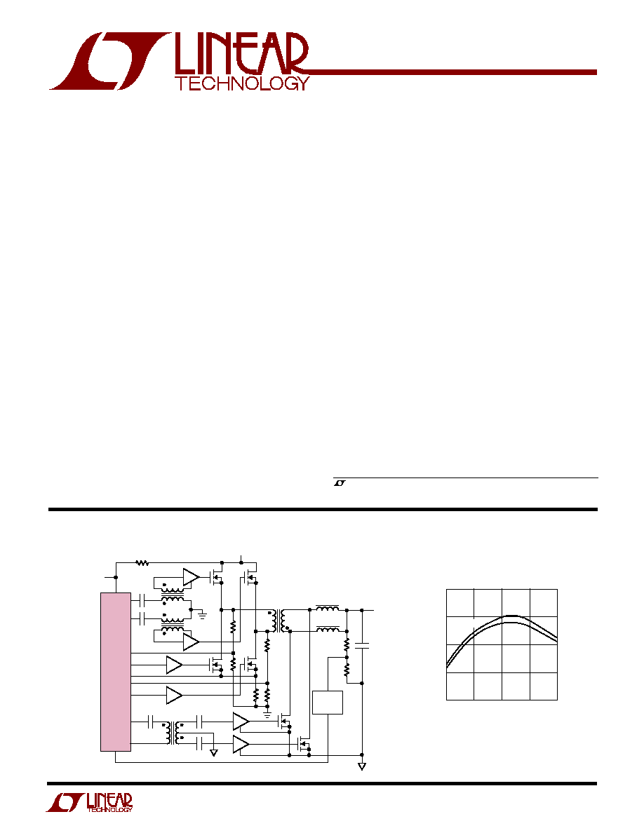
TYPICAL APPLICATIO
U
DESCRIPTIO
U
FEATURES
Synchronous Phase
Modulated Full-Bridge Controller
LOAD CURRENT (A)
0
EFFICIENCY (%)
40
1922 · TA01b
10
20
30
100
90
80
70
60
V
IN
= 36V
V
IN
= 48V
Efficiency
The LTC
®
1922-1 phase shift PWM controller provides all
of the control and protection functions necessary to imple-
ment a high performance, zero voltage switched, phase
shift, full-bridge power converter with synchronous recti-
fication. The part is ideal for developing isolated, low
voltage, high current outputs from a high voltage input
source. The LTC1922-1 combines the benefits of the full-
bridge topology with fixed frequency, zero voltage switch-
ing operation (ZVS). Adaptive ZVS circuity controls the
turn-on signals for each MOSFET independent of internal
and external component tolerances for optimal perfor-
mance.
The LTC1922-1 also provides secondary side synchro-
nous rectifier control. The device uses peak current mode
control with programmable slope comp and leading edge
blanking.
The LTC1922-1 features extremely low operating and
start-up currents to simplify off-line start-up and bias
circuitry. The LTC1922-1 also includes a full range of
protection features and is available in 20-pin through hole
(N) and surface mount (G) packages.
s
Telecommunications, Infrastructure Power Systems
s
Distributed Power Architectures
s
Server Power Supplies
s
High Density Power Modules
s
Adaptive DirectSense
TM
Zero Voltage Switching
s
Integrated Synchronous Rectification Control for
Highest Efficiency
s
Output Power Levels from 50W to Kilowatts
s
Very Low Start-Up and Quiescent Currents
s
Compatible with Voltage Mode and Current Mode
Topologies
s
Programmable Slope Compensation
s
Undervoltage Lockout Circuitry with 4.2V Hysteresis
and Integrated 10.3V Shunt Regulator
s
Fixed Frequency Operation to 1MHz
s
50mA Outputs for Bridge Drive and Secondary Side
Synchronous Rectifiers
s
Soft-Start, Cycle-by-Cycle Current Limiting and
Hiccup Mode Short-Circuit Protection
s
5V, 15mA Low Dropout Regulator
s
20-Pin PDIP and SSOP Packages
, LTC and LT are registered trademarks of Linear Technology Corporation.
DirectSense is a trademark of Linear Technology Corporation.
LTC1922-1
1922 TA01a
ISOLATED
FEEDBACK
V
IN
48V
V
OUT
3.3V
BIAS
SUPPLY
APPLICATIO S
U
LTC1922-1
2
SYMBOL
PARAMETER
CONDITIONS
MIN
TYP
MAX
UNITS
Input Supply
UVLO
Undervoltage Lockout
Measured on V
CC
10.25
10.7
V
UVHY
UVLO Hysteresis
Measured on V
CC
3.8
4.2
V
I
CCST
Start-Up Current
V
CC
= V
UVLO
0.3V
q
145
250
µ
A
I
CCRN
Operating Current
4
7
mA
V
SHUNT
Shunt Regulator Voltage
Current Into V
CC
= 10mA
10.2
10.8
V
R
SHUNT
Shunt Resistance
Current Into V
CC
= 7mA to 17mA
1.5
2
Delay Blocks
DTHR
Delay Pin Threshold
SBUS = 1.5V
1.38
1.50
1.62
V
ADLY and PDLY
SBUS = 2.25V
2.08
2.25
2.42
V
DHYS
Delay Hysteresis Current
SBUS = 1.5V, ADLY/PDLY = 1.6V
1.1
1.3
1.45
mA
ADLY and PDLY
DTMO
Delay Time-Out
SBUS = 1.5V
600
ns
SBUS = 2.25V
900
ns
DZRT
Zero Delay Threshold
Measured on SBUS
3
4.15
5
V
Phase Modulator
ROS
RAMP Offset Voltage
Measured on COMP, RAMP = 0V
0.4
V
I
RMP
RAMP Discharge Current
RAMP = 1V, COMP = 0V
30
50
mA
I
SLP
Slope Compensation Current
Measured on CS, C
T
= 1.5V
35
55
75
µ
A
C
T
= 3V
70
110
150
µ
A
DCMX
Maximum Phase Shift
COMP = 4V
q
95
99.5
%
DCMN
Minimum Phase Shift
COMP = 0V
q
0.1
0.6
%
V
CC
to GND
Low Impedance Source ......................... 0.3V to 10V
(Chip Self Regulates at 10.3V)
All Other Pins to GND
(Low Impedance Source) ..................... 0.3V to 5.5V
V
CC
(Current Fed) .................................................. 25mA
V
REF
Output Current ................................ Self Regulated
Outputs (A, B, C, D, E, F) Current .....................
±
100mA
Operating Temperature Range (Note 5)
LTC1922E ........................................... 40
°
C to 85
°
C
LTC1922I ............................................ 40
°
C to 85
°
C
Storage Temperature Range ................. 65
°
C to 125
°
C
Lead Temperature (Soldering, 10 sec).................. 300
°
C
ORDER PART
NUMBER
T
JMAX
= 125
°
C,
JA
= 110
°
C/W (G)
T
JMAX
= 125
°
C,
JA
= 62
°
C/W (N)
LTC1922EG-1
LTC1922IG-1
LTC1922EN-1
LTC1922IN-1
ABSOLUTE AXI U
RATI GS
W
W
W
U
PACKAGE/ORDER I FOR ATIO
U
U
W
(Note 1)
ELECTRICAL CHARACTERISTICS
The
q
denotes the specifications which apply over the full operating
temperature range, otherwise specifications are at V
CC
= 9.5V, C
T
= 180pF, T
A
= T
MIN
to T
MAX
unless other wise noted.
1
2
3
4
5
6
7
8
9
10
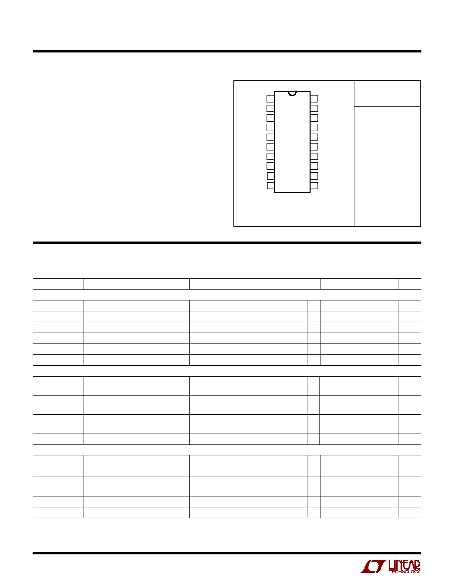
TOP VIEW
G PACKAGE
20-LEAD PLASTIC SSOP
20
19
18
17
16
15
14
13
12
11
SYNC
RAMP
CS
COMP
R
LEB
FB
SS
PDLY
SBUS
ADLY
C
T
GND
OUTA
OUTB
OUTC
V
CC
OUTD
OUTE
OUTF
V
REF
N PACKAGE
20-LEAD PDIP
Consult factory for parts specified with wider operating temperature ranges.
LTC1922-1
3
ELECTRICAL CHARACTERISTICS
The
q
denotes the specifications which apply over the full operating
temperature range, otherwise specifications are at V
CC
= 9.5V, C
T
= 180pF, T
A
= T
MIN
to T
MAX
unless other wise noted.
SYMBOL
PARAMETER
CONDITIONS
MIN
TYP
MAX
UNITS
Oscillator
OSCT
Total Variation
V
CC
= 6.5V to 9.5V
q
236
277
319
kHz
OSCV
C
T
RAMP Amplitude
Measured on C
T
3.6
3.85
4.2
V
OSYT
SYNC Threshold
Measured on SYNC
1.6
1.8
2.2
V
OSYW
Minimum SYNC Pulse Width
Measured at Outputs (Note 2)
6
ns
OSYWX
Maximum SYNC Pulse Width
Measured on Outputs, C
T
= 180pF
1.3
µ
s
OSOP
SYNC Output Pulse Width
Measured on SYNC, R
SYNC
= 5.1k
170
ns
Error Amplifier
V
FB
FB Input Voltage
COMP = 2.5V (Note 3)
1.179
1.204
1.229
V
FBI
FB Input Range
Measured on FB (Note 4)
0.3
2.5
V
AVOL
Open-Loop Gain
COMP = 1V to 3V (Note 3)
70
90
dB
I
IB
Input Bias Current
COMP = 2.5V (Note 3)
5
50
nA
V
OH
Output High
Load on COMP = 100
µ
A
4.7
4.92
V
V
OL
Output Low
Load on COMP = 100
µ
A
0.18
0.4
V
I
SOURCE
Output Source Current
COMP = 2.5V
400
800
µ
A
I
SINK
Output Sink Current
COMP = 2.5V
3
7
mA
Reference
V
REF
Initial Accuracy
T
A
= 25
°
C, Measured on V
REF
4.925
5
5.075
V
REFTV
Total Variation
Line, Load and Temperature
q
4.9
5
5.1
V
REFLD
Load Regulation
Load on V
REF
= 100
µ
A to 5mA
2
15
mV
REFLN
Line Regulation
V
CC
= 6.5V to 9.5V
0.1
10
mV
REFSC
Short-Circuit Current
V
REF
Shorted to GND
18
30
45
mA
Outputs
OUTH(X)
Output High Voltage
I
OUT(X)
= 50mA
7.9
8.4
V
OUTL(X)
Output Low Voltage
I
OUT(X)
= 50mA
0.6
1
V
R
HI(X)
Pull-Up Resistance
I
OUT(X)
= 50mA to 10mA
22
30
R
LO(X)
Pull-Down Resistance
I
OUT(X)
= 50mA to 10mA
12
20
t
r(X)
Rise Time
C
OUT(X)
= 50pF
5
15
ns
t
f(X)
Fall Time
C
OUT(X)
= 50pF
5
15
ns
Current Limit and Shutdown
CLPP
Pulse-by-Pulse Current Limit Threshold
Measured on CS
0.34
0.415
0.48
V
CLSD
Shutdown Current Limit Threshold
Measured on CS
0.55
0.64
0.73
V
SSI
Soft-Start Current
SS = 2.5V
7
12
17
µ
A
SSR
Soft-Start Reset Threshold
Measured on SS
0.7
0.4
0.1
V
FLT
FAULT Reset Threshold
Measured on SS
4.4
4.1
3.8
V
Note 1: Absolute Maximum Ratings are those values beyond which the life
of a device may be impaired.
Note 2: SYNC pulse width is valid from >20ns and <0.4 · (1/f
OSC
),
V
SYNC
= 0V to 5V.
Note 3: FB is driven by a servo loop amplifier to control V
COMP
for these
tests.
Note 4: Set FB to 0.3V, 2.5 and insure that COMP does not phase invert.
Note 5: The LTC1922-1E is guaranteed to meet performance specifications
from 0
°
C to 85
°
C. Specification over the 40
°
C to 85
°
C operating
temperature range are assured by design, characterization and correlation
with statistical process controls. The LTC1922-1I is guaranteed and tested
over the 40
°
C to 85
°
C operating temperature range.
LTC1922-1
4
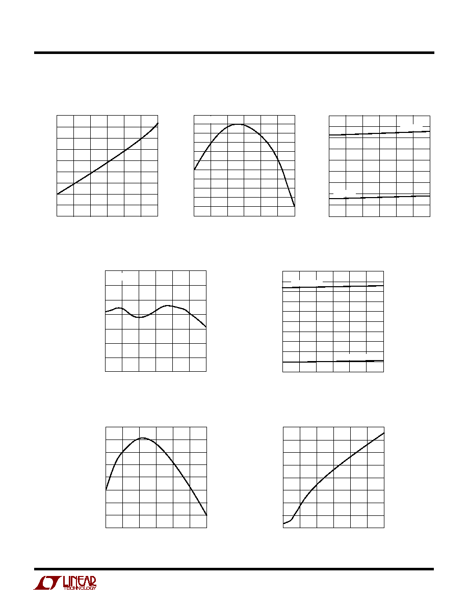
TYPICAL PERFOR A CE CHARACTERISTICS
U
W
V
CC
(V)
0
I
CC
(
µ
A)
100
150
8
1922 · G01
50
0
2
4
6
10
200
T
A
= 25
°
C
I
SHUNT
(mA)
0
V
CC
(V) 10.00
10.25
40
1922 · G02
9.75
9.50
10
20
30
50
10.50
T
A
= 25
°
C
TEMPERATURE (
°
C)
FREQUENCY (kHz)
260
270
80
1922 · G03
250
240
40
60
20
20
0
40
60
100
280
C
T
= 180pF
R
LEB
(k
)
0
BLANK TIME (ns)
350
300
250
200
150
100
50
0
1922 · G04
40
100
20
10
30
50
70
90
60
80
T
A
= 25
°
C
I
REF
(mA)
0
V
REF
(V)
5.05
5.00
4.95
4.90
4.85
4.80
15
25
40
1922 · G05
5
10
20
30
35
T
J
= 25
°
C
T
J
= 85
°
C
T
J
= 40
°
C
TEMPERATURE (
°
C)
V
REF
(V)
4.99
5.00
80
1922 · G03
4.98
4.97
40
60
20
20
0
40
60
100
5.01
Start-Up I
CC
vs V
CC
V
CC
vs I
SHUNT
Oscillator Frequency vs
Temperature
Leading Edge Blanking Time
vs R
LEB
V
REF
vs I
REF
V
REF
vs Temperature
Error Amplifier Gain/Phase
FREQUENCY (Hz)
GAIN (dB)
PHASE (DEG)
180
1M
1922 · G07
270
360
10
1k
100
10k
100k
10M
100
80
60
40
20
0
T
A
= 25
°
C
LTC1922-1
5
TEMPERATURE (
°
C)
55
I
CC
(
µ
A)
160
150
140
130
120
110
100
90
80
70
1922 · G10
25
5
35
95
125
65
TEMPERATURE (
°
C)
55
HYSTERESIS CURRENT (mA)
1922 · G11
25
5
35
95
125
65
1.278
1.276
1.274
1.272
1.270
1.268
1.266
1.264
1.262
1.260
1.258
1.256
SBUS = 1.5V
TEMPERATURE (
°
C)
55
CURRENT (
µ
A)
130
120
110
100
90
80
70
60
50
40
1922 · G12
25
5
35
95
125
65
C
T
= 1.5V
C
T
= 3.0V
TEMPERATURE (
°
C)
55
10.5
10.4
10.3
10.2
10.1
10.0
9.9
9.8
1922 · G13
25
5
35
95
125
65
SHUNT VOLTAGE (V)
I
CC
= 10mA
TEMPERATURE (
°
C)
55
THRESHOLD (V)
2.4
2.3
2.2
2.1
2.0
1.9
1.8
1.7
1.6
1.5
1.4
1922 · G14
25
5
35
95
125
65
SBUS = 1.5V
SBUS = 2.25V
TEMPERATURE (
°
C)
55
FB VOLTAGE (V)
1.202
1.201
1.200
1.199
1.198
1.197
1.196
1.195
1.194
1922 · G15
25
5
35
95
125
65
TEMPERATURE (
°
C)
55
OFFSET (mV)
390
385
380
375
370
365
360
355
350
1922 · G16
25
5
35
95
125
65
TYPICAL PERFOR A CE CHARACTERISTICS
U
W
Start-Up I
CC
vs Temperature
Delay Hysteresis Current vs
Temperature
Slope Current vs Temperature
V
CC
Shunt Voltage vs Temperature
Delay Pin Threshold vs
Temperature
FB Input Voltage vs Temperature
Ramp Offset Voltage vs
Temperature