 | ÐлекÑÑоннÑй компоненÑ: LTC1685 | СкаÑаÑÑ:  PDF PDF  ZIP ZIP |
Äîêóìåíòàöèÿ è îïèñàíèÿ www.docs.chipfind.ru
1
LTC1685
52Mbps, Precision Delay,
RS485 Fail-Safe Transceiver
DESCRIPTIO
N
U
s
Precision Propagation Delay Over Temperature:
Receiver/Driver: 18.5ns
±
3.5ns
s
High Data Rate:
52Mbps
s
Low t
PLH
/t
PHL
Skew:
Receiver/Driver: 500ps Typ
s
7V to 12V RS485 Input Common Mode Range
s
Guaranteed Fail-Safe Receiver Operation Over the
Entire Common Mode Range
s
High Receiver Input Resistance:
22k, Even When
Unpowered
s
Short-Circuit Protected
s
Thermal Shutdown Protected
s
Driver Maintains High Impedance in Three-State or
with Power Off
s
Single 5V Supply
s
Pin Compatible with LTC485
s
45dB CMRR at 26MHz
FEATURES
The LTC
®
1685 is a high speed, precision delay RS485
transceiver that can operate at data rates as high as 52Mbps.
The device also meets the requirements of RS422.
A unique architecture provides very stable propagation
delays and low skew over a wide common mode and
ambient temperature range.
The driver and receiver feature three-state outputs, with
disabled driver outputs maintaining high impedance over
the entire common mode range. A short circuit feature
detects shorted outputs and substantially reduces driver
output current. A similar feature also protects the receiver
output from short circuits. Thermal shutdown circuitry
protects from excessive power dissipation.
The receiver has a fail-safe feature that guarantees a high
output state when the inputs are shorted or are left floating.
The LTC1685 RS485 transceiver guarantees receiver fail-
safe operation over the
entire common mode range ( 7V
to 12V). Input resistance will remain
22k when the device
is unpowered or disabled.
The LTC1685 operates from a single 5V supply and draws
only 7mA of supply current.
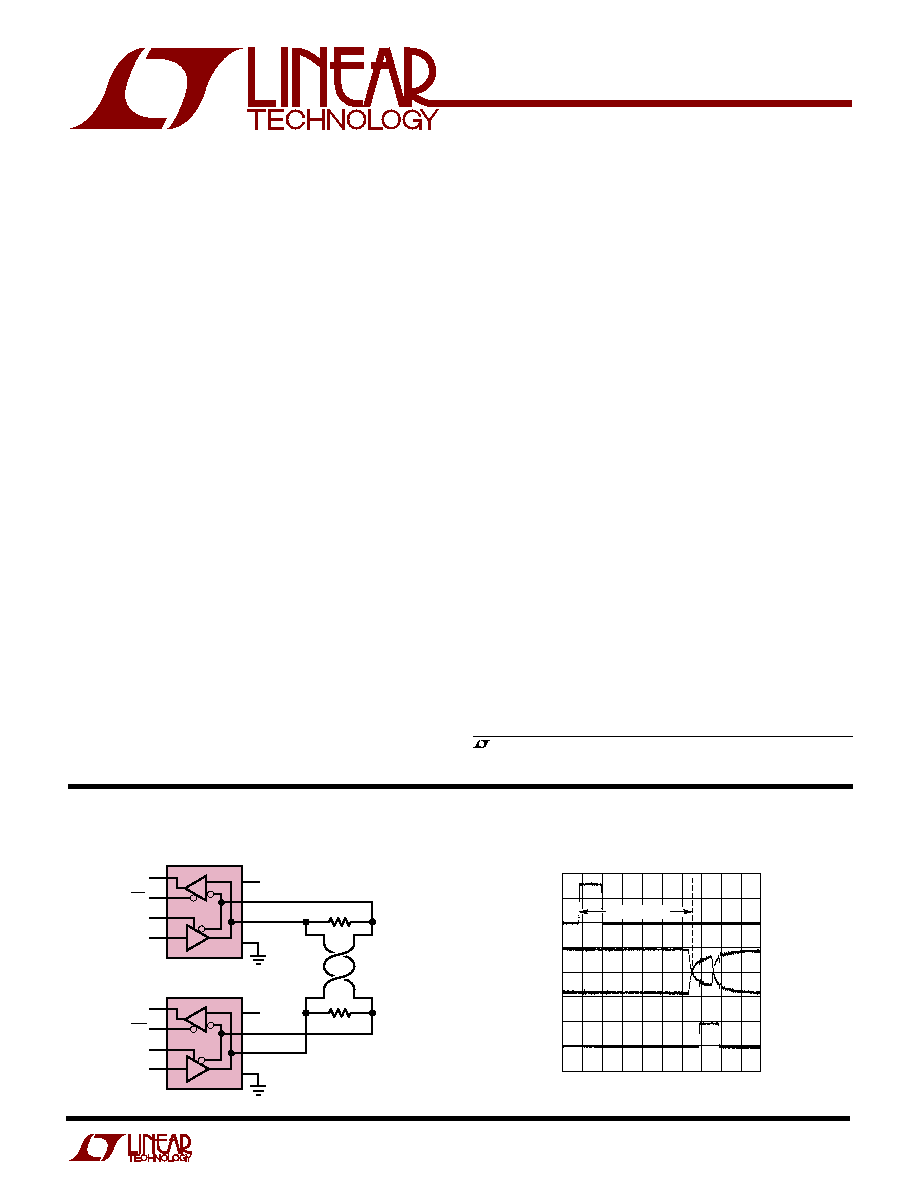
10Mbps Data Pulse
400ft Category 5 UTP
1685 TA02
DRIVER INPUT
RECEIVER
INPUT
RECEIVER
OUTPUT
100ns/DIV
1V/DIV
2V/DIV
5V/DIV
CABLE DELAY
, LTC and LT are registered trademarks of Linear Technology Corporation.
APPLICATIO
N
S
U
s
High Speed RS485/RS422 Transceivers
s
Level Translator
s
Backplane Transceiver
s
STS-1/OC-1 Data Transceiver
s
Fast-20, Fast-40 SCSI Transceivers
TYPICAL APPLICATIO
N
U
V
CC1
GND1
R
RO1
RE1
DE1
DI1
D
Rt
Rt
1685 TA01
V
CC2
GND2
R
RO2
RE2
DE2
DI2
D
2
LTC1685
W
U
U
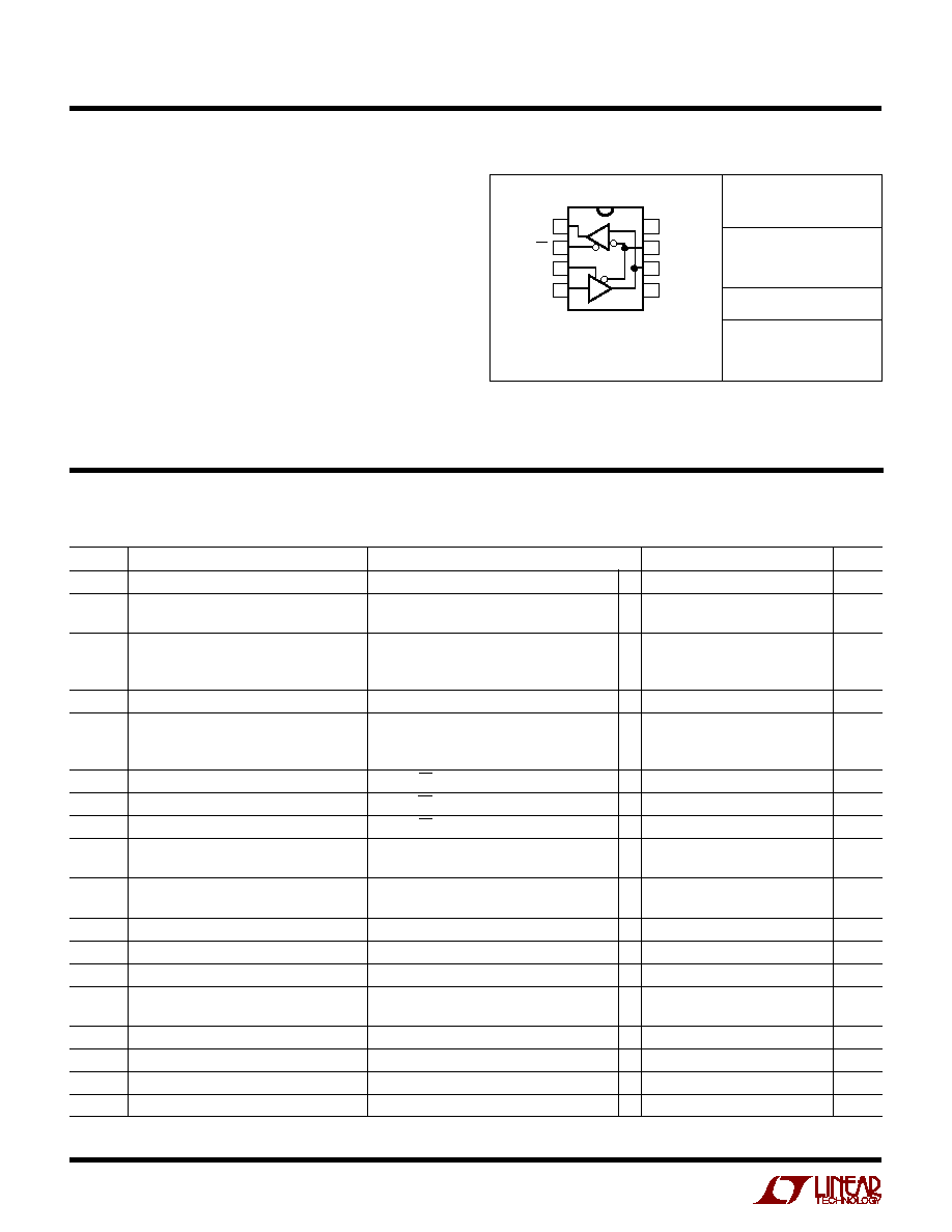
PACKAGE/ORDER I FOR ATIO
A
U
G
W
A
W
U
W
A
R
BSOLUTE
XI
TI
S
(Note 1)
Supply Voltage (V
DD
) .............................................. 10V
Control Input Currents .................... 100mA to 100mA
Control Input Voltages .................. 0.5V to V
DD
+ 0.5V
Driver Input Voltages .................... 0.5V to V
DD
+ 0.5V
Driver Output Voltages .................................. +12V/ 7V
Receiver Input Voltages ................................. +12V/ 7V
Receiver Output Voltages ............. 0.5V to V
DD
+ 0.5V
Receiver Input Differential ...................................... 10V
Short-Circuit Duration (Driver V
OUT
: 7V to 10V,
Receiver V
OUT
: 0V to V
DD
) ............................... Indefinite
Operating Temperature Range .................... 0
°
C to 70
°
C
Storage Temperature Range ................ 65
°
C to 150
°
C
Lead Temperature (Soldering, 10 sec)................. 300
°
C
ORDER PART
NUMBER
1
2
3
4
8
7
6
5
TOP VIEW
V
DD
B
A
GND
S8 PACKAGE
8-LEAD PLASTIC SO
RO
RE
DE
DI
R
D
T
JMAX
= 125
°
C,
JA
= 150
°
C/ W
Consult factory for Industrial and Military grade parts.
S8 PART MARKING
DC ELECTRICAL CHARACTERISTICS
V
DD
= 5V
±
5%, unless otherwise noted. (Notes 2, 3)
SYMBOL
PARAMETER
CONDITIONS
MIN
TYP
MAX
UNITS
V
OD1
Differential Driver Output (Unloaded)
I
OUT
= 0
q
V
DD
V
V
OD2
Differential Driver Output (With Load)
R = 50
(RS422)
2
V
R = 27
(RS485), Figure 1
q
1.5
V
DD
V
V
OD
Change in Magnitude of Driver Differential
R = 27
or 50
, Figure 1
q
0.2
V
Output Voltage for Complementary
Output States
V
OC
Driver Common Mode Output Voltage
R = 27
or 50
, V
DD
= 5V, Figure 1
q
2
3
V
V
OC
Change in Magnitude of Driver Common
R = 27
or 50
, Figure 1
q
0.2
V
Mode Output Voltage for Complementary
Output States
V
IH
Input High Voltage
DE, DI, RE
q
2
V
V
IL
Input Low Voltage
DE, DI, RE
q
0.8
V
I
IN1
Input Current
DE, DI, RE
q
1
1
µ
A
I
IN2
Input Current (A, B)
V
A
, V
B
= 12V, DE = 0, V
DD
= 0V or 5.25V
q
500
µ
A
V
A
, V
B
= 7V, DE = 0, V
DD
= 0V or 5.25V
q
500
µ
A
V
TH
Differential Input Threshold Voltage
7V
V
CM
12V
q
0.3
0.3
V
for Receiver
V
TH
Receiver Input Hysteresis
V
CM
= 0V
25
mV
V
OH
Receiver Output High Voltage
I
OUT
= 4mA, V
ID
= 300mV
q
3.5
4.8
V
V
OL
Receiver Output Low Voltage
I
OUT
= 4mA, V
ID
= 300mV
q
0.4
V
I
OZR
Three-State (High Impedance) Output
0.4V
V
OUT
2.4V
q
1
1
µ
A
Current at Receiver
I
DD
Supply Current
No Load, Pins 2, 3, 4 = 0V or V
DD
q
7
12
mA
I
OSD1
Driver Short-Circuit Current, V
OUT
= HIGH
V
OUT
= 7V or 10V (Note 5)
q
20
mA
I
OSD2
Driver Short-Circuit Current, V
OUT
= LOW
V
OUT
= 7V or 10V (Note 5)
q
20
mA
I
OSR
Receiver Short-Circuit Current
V
OUT
= 0V or V
DD
(Note 5)
q
20
mA
LTC1685CS8
1685
3
LTC1685
DC ELECTRICAL CHARACTERISTICS
V
DD
= 5V
±
5%, unless otherwise noted. (Notes 2, 3)
SYMBOL
PARAMETER
CONDITIONS
MIN
TYP
MAX
UNITS
R
IN
Input Resistance
7V
V
CM
12V
q
22
k
C
IN
Input Capacitance
A, B Inputs, D, DE, RE
3
pF
Open-Circuit Input Voltage, Figure 5
V
DD
= 5V (Note 4)
q
3.2
3.3
3.4
V
Fail-Safe
Time to Detect Fail-Safe Condition
2
µ
s
Time
CMRR
Receiver Input Common Mode
V
CM
= 2.6V, f = 26MHz
45
dB
Rejection Ratio
C
LOAD
Receiver and Driver Output
(Note 4)
q
500
pF
Load Capacitance
V
DD
= 5V, unless otherwise noted. (Notes 2, 3)
SWITCHI
N
G CHARACTERISTICS
U
The
q
denotes specifications which apply over the full operating
temperature range.
Note 1: Absolute Maximum Ratings are those values beyond which the life
of a device may be impaired.
Note 2: All currents into the device pins are positive; all currents out of the
device pins are negative.
Note 3: All typicals are given for V
DD
= 5V, T
A
= 25
°
C.
Note 4: Guaranteed by design, but not tested.
Note 5: Short-circuit current does not represent output drive capability.
When the output detects a short-circuit condition, output drive current is
significantly reduced (from hundreds of mA to 20mA max) until the short
is removed.
SYMBOL
PARAMETER
CONDITIONS
MIN
TYP
MAX
UNITS
t
PLH
, t
PHL
Driver Input-to-Output Propagation Delay
R
DIFF
= 54
, C
L1
= C
L2
= 100pF,
q
15
18.5
22
ns
Figures 3, 5
t
SKEW
Driver Output A-to-Output B Skew
R
DIFF
= 54
, C
L1
= C
L2
= 100pF,
500
ps
Figures 3, 5
t
r
, t
f
Driver Rise/Fall Time
R
DIFF
= 54
, C
L1
= C
L2
= 100pF,
3.5
ns
Figures 3, 5
t
ZH
Driver Enable to Output High
C
L
= 100pF, S2 Closed, Figures 4, 6
q
25
50
ns
t
ZL
Driver Enable to Output Low
C
L
= 100pF, S1 Closed, Figures 4, 6
q
25
50
ns
t
LZ
Driver Disable from Low
C
L
= 15pF, S1 Closed, Figures 4, 6
q
25
50
ns
t
HZ
Driver Disable from High
C
L
= 15pF, S2 Closed, Figures 4, 6
q
25
50
ns
t
PLH
, t
PHL
Receiver Input-to-Output Propagation Delay
C
L
= 15pF, Figures 3, 7
q
15
18.5
22
ns
t
SQD
Receiver Skew
t
PLH
t
PHL
C
L
= 15pF, Figures 3, 7
500
ps
t
ZL
Receiver Enable to Output Low
C
L
= 15pF, S1 Closed, Figures 2, 8
q
25
50
ns
t
ZH
Receiver Enable to Output High
C
L
= 15pF, S2 Closed, Figures 2, 8
q
25
50
ns
t
LZ
Receiver Disable from Low
C
L
= 15pF, S1 Closed, Figures 2, 8
q
25
50
ns
t
HZ
Receiver Disable from High
C
L
= 15pF, S2 Closed, Figures 2, 8
q
25
50
ns
Maximum Receiver Input
(Note 4)
q
2000
ns
Rise/Fall Times
t
PKG-PKG
Package-to-Package Skew
Same Temperature (Note 4)
1.5
ns
Minimum Input Pulse Width
V
DD
= 5V
±
5% (Note 4)
q
17
19.2
ns
Maximum Data Rate
V
DD
= 5V
±
5% (Note 4)
q
52
60
Mbps
Maximum Input Frequency
V
DD
= 5V
±
5% (Note 4)
q
26
30
MHz
4
LTC1685
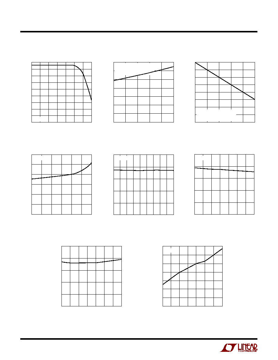
TYPICAL PERFOR
M
A
N
CE CHARACTERISTICS
U
W
FREQUENCY (Hz)
10
42.0
COMMON MODE REJECTION RATIO (dB)
42.5
43.5
44.0
44.5
46.5
1685 G01
43.0
1k
100k
1M
45.0
45.5
46.0
T
A
= 25
°
C
Receiver Input CMRR
TEMPERATURE (
°
C)
25
SUPPLY CURRENT (mA)
53
54
55
50
100
1685 G03
52
51
50
0
25
75
56
57
58
BOTH DRIVER AND RECEIVER
ENABLED AND LOADED
25Mbps DATA RATE
DATA RATE (Mbps)
1
50
60
70
40
30
1685 G02
40
30
10
20
50
20
10
0
SUPPLY CURRENT (mA)
BOTH DRIVER AND RECEIVER
ENABLED AND LOADED
T
A
= 25
°
C
Supply Current vs Data Rate
Supply Current vs Temperature
Receiver Propagation Delay
vs Load Capacitance
Receiver Propagation Delay
vs Common Mode
LOAD CAPACITANCE (pF)
5
0
PROPAGATION DELAY (ns)
5
10
15
20
30
15
25
35
55
1685 G04
105
205
25
T
A
= 25
°
C
RECEIVER COMMON MODE (V)
7
0
PROPAGATION DELAY (ns)
5
15
20
25
2
2
4
12
1685 G05
10
4
0
6
8
10
T
A
= 25
°
C
Receiver Propagation Delay
vs Input Overdrive
RECEIVER INPUT OVERDRIVE (V)
0.3
0.5
0
RECEIVER PROPAGATION DELAY (ns)
10
25
0.7
1.25
1.5
1685 G06
5
20
15
1.0
2.0
2.5
T
A
= 25
°
C
Receiver Maximum Data Rate
vs Input Overdrive
Receiver Propagation Delay
vs Temperature
TEMPERATURE (
°
C)
50
25
0
PROPAGATION DELAY (ns)
10
25
0
50
75
1680 G09
5
20
15
25
100
125
RECEIVER INPUT DIFFERENTIAL (V)
0.3
40
50
70
0.6
1.0
1685 G10
30
20
0.4
0.5
0.7
1.5
2.5
10
0
60
DATA RATE (Mbps)
T
A
= 25
°
C
5
LTC1685
TYPICAL PERFOR
M
A
N
CE CHARACTERISTICS
U
W
DI (Pin 4): Driver Input. Controls the states of the A and
B outputs only if DE = High. If DE = Low, DI will have no
effect on A and B pins. Do not float.
GND (Pin 5): Ground.
A (Pin 6): Noninverting Receiver Input/Driver Output.
B (Pin 7): Inverting Receiver Input/Driver Output.
V
DD
(Pin 8): Positive Supply, 5V to
±
5%. Bypass with
0.1
µ
F ceramic capacitor.
PI
N
FU
N
CTIO
N
S
U
U
U
RO (Pin 1): Receiver Output. If A
B by 300mV, then RO
will be high. If A
B by 300mV, then RO will be low.
RE (Pin 2): Receiver Enable. RE = Low enables the
receiver. RE = High forces receiver output into high
impedance state. Do not float.
DE (Pin 3): Driver Enable. DE = High enables the driver.
DE = Low will force the driver output into a high impedance
state and the device will function as a line receiver if RE is
also low. Do not float.
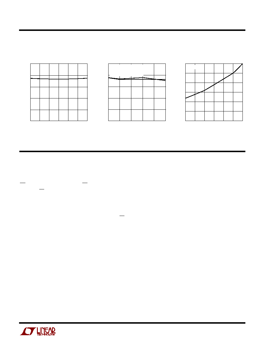
Driver Propagation Delay
vs Temperature
TEMPERATURE (
°
C)
20
0
PROPAGATION DELAY (ns)
5
10
15
20
25
0
20
40
60
1685 G07
80
100
Driver Propagation Delay
vs Driver Input Voltage
DRIVER INPUT VOLTAGE (V)
2.5
PROPAGATION DELAY (ns)
15
20
25
4.5
1685 G08
10
5
0
3.0
3.5
4.0
5.0
t
LH
V
DD
= 5V
INPUT THRESHOLD = 1.5V
T
A
= 25
°
C
t
HL
Driver Propagation Delay
vs Capacitive Load
LOAD CAPACITANCE (pF)
5
16.0
PROPAGATION DELAY (ns)
16.5
17.0
17.5
18.0
19.0
15
25
50
75
1685 G11
100
150
18.5
T
A
= 25
°
C