 | ÐлекÑÑоннÑй компоненÑ: LTC1335 | СкаÑаÑÑ:  PDF PDF  ZIP ZIP |
Äîêóìåíòàöèÿ è îïèñàíèÿ www.docs.chipfind.ru
1
LTC1321/LTC1322/LTC1335
RS232/EIA562/RS485
Transceivers
S
FEATURE
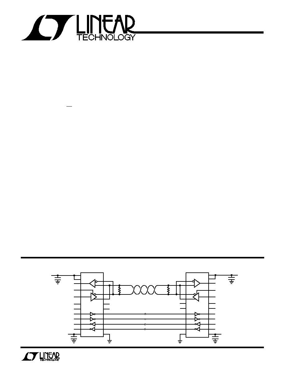
The LTC1321/LTC1322/LTC1335 are low power CMOS
bidirectional transceivers, each featuring two reconfigurable
interface ports. Each can be configured as two RS485
differential ports, as two single-ended ports, or as one
RS485 differential port and one single-ended port. The
LTC1321/LTC1322 can provide RS232 or EIA562 compat-
ible single-ended outputs; the LTC1335 provides EIA562
compatible outputs and additionally includes an output
enable pin, allowing the receiver logic level outputs to be
three-stated.
The RS232/EIA562 transceivers operate to 120kbaud and
are in full compliance with EIA/TIA-562 specification. The
RS485 transceivers operate to 10Mbaud and are in full
compliance with RS485 and RS422 specifications. All
interface drivers feature short-circuit and thermal shut-
down protection. An enable pin allows RS485 driver
outputs to be forced into high impedance which is main-
tained even when the outputs are forced beyond supply
rails or power is off. Both driver outputs and receiver
inputs feature
±
10kV ESD protection. A loopback mode
connects the driver outputs back to the receiver inputs for
diagnostic self-test.
The LTC1321/LTC1322 can support RS232 voltage levels
when 6.5V
V
DD
10V and 6.5V
V
EE
10V. The
LTC1335 supports receiver output enable but not RS232
levels. A shutdown mode reduces the I
CC
supply current
to 15
µ
A.
D
U
ESCRIPTIO
APPLICATIO
N
S
U
s
Low Power RS485/RS422/EIA562/RS232 Interface
s
Cable Repeater
s
Level Translator
s
LTC1321: 2-EIA562/RS232 Transceivers/2-RS485
Transceivers
s
LTC1322: 4-EIA562/RS232 Transceivers/2-RS485
Transceivers
s
LTC1335: 4-EIA562 Transceivers/2-RS485
Transceivers with OE
s
LTC1321/LTC1322 Have the Same Pinout as
SP301/SP302
s
LTC1335 Features Receiver Three-State Outputs
s
Low Supply Current: 1mA Typical
s
15
µ
A Supply Current in Shutdown
s
120kBaud in EIA/TIA-562 or RS232 Mode
s
10MBaud in RS485/RS422 Mode
s
Self-Testing Capability in Loopback Mode
s
Power-Up/Down Glitch-Free Outputs
s
Driver Maintains High Impedance in Three-State,
Shutdown or With Power Off
s
Thermal Shutdown Protection
s
I/O Lines Can Withstand
±
25V
s
Withstands Repeated 10kV ESD Pulses
U
A
O
PPLICATI
TYPICAL
19
5V
6
5V
7
5V
18
0V
1
24
V
CC2
5V
1
24
V
CC1
5V
120
2
LTC1322
1321/22/35 TA01
RX OUT
21
RS485 INTERFACE
DR ENABLE
3
4
5
12
22
DR IN
20
13
V
EE1
5V
11
19
LTC1322
RX OUT
16
5V
DR ENABLE
10
9
8
7
6
12
15
DR IN
17
5V
18
13
V
EE2
5V
120
4000-FT 24-GAUGE TWISTED PAIR
5V
0V
8
DR IN
17
3
22
RX OUT
11
14
RX OUT
4
DR IN
21
EIA562 INTERFACE
9
DR IN
16
2
23
RX OUT
10
15
RX OUT
5
DR IN
20
2
LTC1321/LTC1322/LTC1335
A
U
G
W
A
W
U
W
A
R
BSOLUTE
XI
TI
S
Supply Voltage
V
CC
.................................................................... 6.5V
V
DD
(LTC1321/LTC1322 Only) ........................... 10V
V
EE
................................................................... 10V
Input Voltage
Drivers ................................... 0.3V to (V
CC
+ 0.3V)
Receivers ............................................. 25V to 25V
ON/OFF, LB, SEL1,
SEL2, OE ............................ 0.3V to (V
CC
+ 0.3V)
Output Voltage
Drivers ................................................. 25V to 25V
Receivers ............................... 0.3V to (V
CC
+ 0.3V)
Output Short-Circuit Duration ......................... Indefinite
Operating Temperature Range
LTC1321C/LTC1322C/LTC1335C ......... 0
°
C to 70
°
C
LTC1321I/LTC1322I/LTC1335I ......... 40
°
C to 85
°
C
Storage Temperature Range ................ 65
°
C to 150
°
C
Lead Temperature (Soldering, 10 sec)................ 300
°
C
W
U
U
PACKAGE/ORDER I FOR ATIO
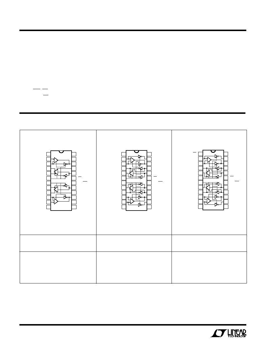
2 RS485 DRIVERS/RECEIVERS
2 EIA/TIA-562 DRIVERS/RECEIVERS
2 RS485 DRIVERS/RECEIVERS
4 EIA/TIA-562 DRIVERS/RECEIVERS
2 RS485 DRIVERS/RECEIVERS
4 EIA/TIA-562 DRIVERS/RECEIVERS
1
2
3
4
5
6
7
8
9
10
11
12
TOP VIEW
S PACKAGE
24-LEAD PLASTIC SOL
24
23
22
21
20
19
18
17
16
15
14
13
V
DD
B1
A1
Z1
Y1
SEL1
SEL2
Y2
Z2
A2
B2
GND
V
CC
NC
R
A1
DE1
D
Y1
LB
ON/OFF
D
Y2
DE2
R
A2
NC
V
EE
N PACKAGE
24-LEAD PLASTIC DIP
1
2
3
4
5
6
7
8
9
10
11
12
TOP VIEW
24
23
22
21
20
19
18
17
16
15
14
13
V
DD
B1
A1
Z1
Y1
SEL1
SEL2
Y2
Z2
A2
B2
GND
V
CC
R
B1
R
A1
D
Z1
/DE1
D
Y1
LB
ON/OFF
D
Y2
D
Z2
/DE2
R
A2
R
B2
V
EE
S PACKAGE
24-LEAD PLASTIC SOL
N PACKAGE
24-LEAD PLASTIC DIP
1
2
3
4
5
6
7
8
9
10
11
12
TOP VIEW
24
23
22
21
20
19
18
17
16
15
14
13
OE
B1
A1
Z1
Y1
SEL1
SEL2
Y2
Z2
A2
B2
GND
V
CC
R
B1
R
A1
D
Z1
/DE1
D
Y1
LB
ON/OFF
D
Y2
D
Z2
/DE2
R
A2
R
B2
V
EE
S PACKAGE
24-LEAD PLASTIC SOL
N PACKAGE
24-LEAD PLASTIC DIP
T
JMAX
= 125
°
C,
JA
= 75
°
C/W (N)
T
JMAX
= 125
°
C,
JA
= 85
°
C/W (S)
T
JMAX
= 125
°
C,
JA
= 75
°
C/W (N)
T
JMAX
= 125
°
C,
JA
= 85
°
C/W (S)
T
JMAX
= 125
°
C,
JA
= 75
°
C/W (N)
T
JMAX
= 125
°
C,
JA
= 85
°
C/W (S)
ORDER PART
NUMBER
ORDER PART
NUMBER
ORDER PART
NUMBER
LTC1321CN
LTC1321CS
LTC1321IN
LTC1321IS
LTC1335CN
LTC1335CS
LTC1335IN
LTC1335IS
LTC1322CN
LTC1322CS
LTC1322IN
LTC1322IS
Consult factory for Military grade parts.
3
LTC1321/LTC1322/LTC1335
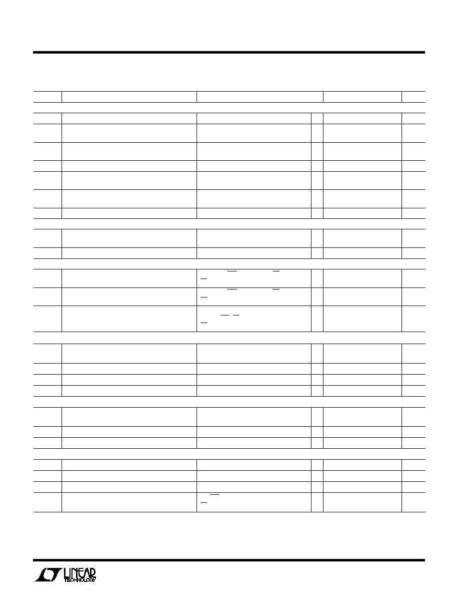
DC ELECTRICAL CHARACTERISTICS
V
CC
= V
DD
(LTC1321/LTC1322) = 5V
±
5%, V
EE
= 5V
±
5% (Notes 2, 3)
SYMBOL
PARAMETER
CONDITIONS
MIN
TYP
MAX
UNITS
RS485 Driver (SEL1 = SEL2 = HIGH)
V
OD1
Differential Driver Output Voltage (Unloaded)
I
O
= 0
q
5
V
V
OD2
Differential Driver Output Voltage (With Load)
Figure 1, R = 50
(RS422)
q
2.0
5
V
Figure 1, R = 27
(RS485)
q
1.5
5
V
V
OD
Change in Magnitude of Driver Differential
Figure 1, R = 27
or R = 50
q
0.2
V
Output Voltage for Complementary Output States
V
OC
Driver Common-Mode Output Voltage
Figure 1, R = 27
or R = 50
q
3
V
V
OC
Change in Magnitude of Driver Common-Mode
Figure 1, R = 27
or R = 50
q
0.2
V
Output Voltage for Complementary Output States
I
OSD
Driver Short-Circuit Current
7V
V
O
12V, V
O
= HIGH
q
35
250
mA
7V
V
O
12V, V
O
= LOW (Note 4)
q
10
250
mA
I
OZD
Three-State Output Current (Y, Z)
7V
V
O
12V
q
±
5
±
500
µ
A
EIA/TIA-562 Driver (SEL1 = SEL2 = LOW)
V
O
Output Voltage Swing
Figure 4, R
L
= 3k, Positve
q
3.7
4.2
V
Figure 4, R
L
= 3k, Negative
q
3.7
4.3
V
I
OSD
Output Short-Circuit Current
V
O
= 0V
q
±
11
±
60
mA
Driver Inputs and Control Inputs
V
IH
Input High Voltage
D, DE, ON/OFF, SEL1, SEL2, LB
q
2
V
OE (LTC1335)
q
2
V
V
IL
Input Low Voltage
D, DE, ON/OFF, SEL1, SEL2, LB
q
0.8
V
OE (LTC1335)
q
0.8
V
I
IN
Input Current
D, SEL1, SEL2
q
±
10
µ
A
DE, ON/OFF, LB
q
4
15
µ
A
OE (LTC1335)
q
4
15
µ
A
RS485 Receiver (SEL1 = SEL2 = HIGH)
V
TH
Differential Input Threshold Voltage
7V
V
CM
7V, Commercial
q
0.2
0.2
V
7V
V
CM
7V, Industrial
q
0.3
0.3
V
V
TH
Input Hysteresis
V
CM
= 0V
q
70
mV
I
IN
Input Current (A, B)
7V
V
IN
12V
q
±
1
mA
R
IN
Input Resistance
7V
V
IN
12V
q
12
24
k
EIA/TIA-562 Receiver (SEL1 = SEL2 = LOW)
V
TH
Receiver Input Voltage Threshold
Input Low Threshold
q
0.8
1.1
V
Input High Threshold
q
1.7
2.4
V
V
TH
Receiver Input Hysteresis
q
0.1
0.6
1.0
V
R
IN
Receiver Input Resistance
V
IN
=
±
10V
3
5
7
k
Receiver Output
V
OH
Receiver Output High Voltage
I
O
= 3mA, V
IN
= 0V, SEL1 = SEL2 = LOW
q
3.5
4.6
V
V
OL
Receiver Output Low Voltage
I
O
= 3mA, V
IN
= 3V, SEL1 = SEL2 = LOW
q
0.2
0.4
V
I
OSR
Short-Circuit Current
0V
V
O
V
CC
q
7
85
mA
I
OZR
Three-State Output Current
ON/OFF = 0V
q
±
10
µ
A
OE = V
CC
(LTC1335)
q
±
10
µ
A
4
LTC1321/LTC1322/LTC1335
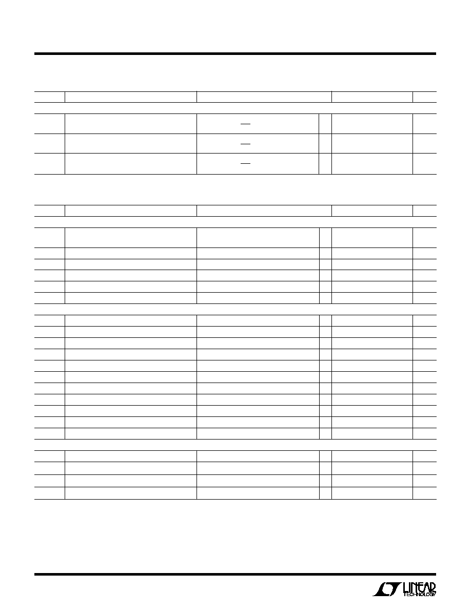
DC ELECTRICAL CHARACTERISTICS
SYMBOL
PARAMETER
CONDITIONS
MIN
TYP
MAX
UNITS
Supply Currents
I
CC
V
CC
Supply Current
No Load (SEL1 = SEL2 = HIGH)
q
1000
2000
µ
A
Shutdown, ON/OFF = 0V
q
15
50
µ
A
I
DD
V
DD
Supply Current (LTC1321/LTC1322)
No Load (SEL1 = SEL2 = LOW)
q
300
1000
µ
A
Shutdown, ON/OFF = 0V
q
0.1
50
µ
A
I
EE
V
EE
Supply Current
No Load (SEL1 = SEL2 = HIGH)
q
1000
2000
µ
A
Shutdown, ON/OFF = 0V
q
0.1
50
µ
A
DC ELECTRICAL CHARACTERISTICS
V
CC
= V
DD
(LTC1321/LTC1322) = 5V
±
5%, V
EE
= 5V
±
5% (Notes 2, 3)
AC
V
CC
= V
DD
(LTC1321/LTC1322) = 5V
±
5%, V
EE
= 5V
±
5% (Notes 2, 3)
SYMBOL
PARAMETER
CONDITIONS
MIN
TYP
MAX
UNITS
EIA/TIA-562 Mode (SEL1 = SEL2 = LOW)
SR
Slew Rate
Figure 4, R
L
= 3k, C
L
= 15pF
q
14
30
V/
µ
s
Figure 4, R
L
= 3k, C
L
= 1000pF
q
4
7
V/
µ
s
t
T
Transition Time
Figure 4, R
L
= 3k, C
L
= 2500pF
q
0.22
1.9
3.1
µ
s
t
PLH
Driver Input to Output
Figures 4,10, R
L
= 3k, C
L
= 15pF
q
0.6
4
µ
s
t
PHL
Driver Input to Output
Figures 4,10, R
L
= 3k, C
L
= 15pF
q
0.6
4
µ
s
t
PLH
Receiver Input to Output
Figures 5,11
q
0.3
6
µ
s
t
PHL
Receiver Input to Output
Figures 5,11
q
0.4
6
µ
s
RS485 Mode (SEL1 = SEL2 = HIGH)
t
PLH
Driver Input to Output
Figures 2,7, R
L
= 54
, C
L
= 100pF
q
20
40
70
ns
t
PHL
Driver Input to Output
Figures 2,7, R
L
= 54
, C
L
= 100pF
q
20
40
70
ns
t
SKEW
Driver Output to Output
Figures 2,7, R
L
= 54
, C
L
= 100pF
q
5
15
ns
t
r
, t
f
Driver Rise or Fall Time
Figures 2,7, R
L
= 54
, C
L
= 100pF
q
3
15
40
ns
t
ZL
Driver Enable to Output Low
Figures 3,8, C
L
= 100pF, S1 Closed
q
50
90
ns
t
ZH
Driver Enable to Output High
Figures 3,8, C
L
= 100pF, S2 Closed
q
50
90
ns
t
LZ
Driver Disable from Low
Figures 3,8, C
L
= 15pF, S1 Closed
q
50
90
ns
t
HZ
Driver Disable from High
Figures 3,8, C
L
= 15pF, S2 Closed
q
60
90
ns
t
PLH
Receiver Input to Output
Figures 2,9, R
L
= 54
, C
L
= 100pF
q
20
60
140
ns
t
PHL
Receiver Input to Output
Figures 2,9, R
L
= 54
, C
L
= 100pF
q
20
70
140
ns
t
SKEW
Differential Receiver Skew,
t
PLH
-t
PHL
Figures 2,9, R
L
= 54
, C
L
= 100pF
q
10
ns
Receiver Output Enable/Disable (LTC1335)
t
ZL
Receiver Enable to Output Low
Figures 6,12, C
L
= 15pF, S1 Closed
q
40
90
ns
t
ZH
Receiver Enable to Output High
Figures 6,12, C
L
= 15pF, S2 Closed
q
40
90
ns
t
LZ
Receiver Disable from Low
Figures 6,12, C
L
= 15pF, S1 Closed
q
40
90
ns
t
HZ
Receiver Disable from High
Figures 6,12, C
L
= 15pF, S2 Closed
q
50
90
ns
The
q
denotes specifications which apply over the full operating
temperature range.
Note 1: Absolute maximum ratings are those values beyond which the
safety of the device cannot be guaranteed.
Note 2: All currents into device pins are positive; all currents out of device
pins are negative. All voltages are referenced to device ground unless
otherwise specified.
Note 3: All typicals are given at V
CC
= V
DD
(LTC1321/LTC1322) = 5V,
V
EE
= 5V, and T
A
= 25
°
C.
Note 4: Short-circuit current for RS485 driver output low state folds back
above V
CC
. Peak current occurs around V
O
= 3V.
5
LTC1321/LTC1322/LTC1335
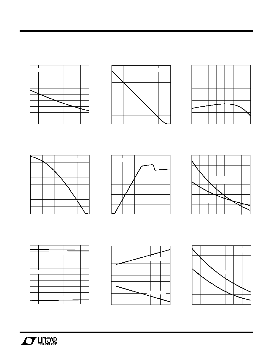
RS485 Driver Differential Output
Voltage vs Temperature
TEMPERATURE (°C)
50
DIFFERENTIAL OUTPUT VOLTAGE (V)
2.6
2.5
2.4
2.3
2.2
2.1
2.0
1.9
1.8
1.7
1.6
0
50
75
1321 G01
25
25
100
125
R
L
= 54
RS485 Driver Output High Voltage
vs Output Current
EIA562 Driver Output Voltage
vs Temperature
OUTPUT VOLTAGE (V)
0
OUTPUT CURRENT (mA)
3
5
1321 G04
1
2
4
80
70
60
50
40
30
20
10
0
T
A
= 25°C
TEMPERATURE (°C)
50
OUTPUT VOLTAGE (V)
5
4
3
2
1
0
1
2
3
4
5
0
50
75
1321 G07
25
25
100
125
R
L
= 3k
OUTPUT HIGH
OUTPUT LOW
TYPICAL PERFOR
M
A
N
CE CHARACTERISTICS
U
W
TEMPERATURE (°C)
50
TIME (
µ
s)
15
12
9
6
3
0
0
50
75
1321 G03
25
25
100
125
RS485 Driver Skew vs
Temperature
EIA562 Driver Output Short-Circuit
Current vs Temperature
TEMPERATURE (°C)
50
OUTPUT SHORT-CIRCUIT CURRENT (mA)
18
16
14
12
10
8
6
25
75
1321 G09
25
0
50
100
125
SOURCE
V
OUT
= 0V
SINK
DIFFERENTIAL OUTPUT VOLTAGE (V)
0
70
60
50
40
30
20
10
0
3
4
1321 G02
1
2
5
DIFFERENTIAL OUTPUT CURRENT (mA)
T
A
= 25°C
RS485 Driver Differential Output
Current vs Output Voltage
OUTPUT VOLTAGE (V)
0
OUTPUT CURRENT (mA)
120
100
80
60
40
20
0
1
2
3
4
1321 G05
5
T
A
= 25°C
RS485 Driver Output Low Voltage
vs Output Current
EIA562 Driver Output Voltage
vs Supply Voltage
V
DD
SUPPLY VOLTAGE (V)
4
OUTPUT VOLTAGE (V)
5
6
7
8
1321 G08
9
10
8
6
4
2
0
2
4
6
8
10
10
R
L
= 3k
T
A
= 25°C
V
EE
= V
DD
OUTPUT HIGH
OUTPUT LOW
RS485 Driver Output Short-Circuit
Current vs Temperature
TEMPERATURE (°C)
50
OUTPUT SHORT-CIRCUIT CURRENT (mA)
160
140
120
100
80
60
40
25
75
1321 G19
25
0
50
100
125
SOURCE
(V
OUT
= 0V)
SINK
(V
OUT
= 5V)