 | ÐлекÑÑоннÑй компоненÑ: LTC1153 | СкаÑаÑÑ:  PDF PDF  ZIP ZIP |
Äîêóìåíòàöèÿ è îïèñàíèÿ www.docs.chipfind.ru
1
LTC1153
D
U
ESCRIPTIO
S
FEATURE
Auto-Reset
Electronic Circuit Breaker
s
Programmable Trip Delay: 15
µ
s to >100ms
s
Programmable Trip Current: 1mA to >20A
s
Programmbale Auto-Reset Time: 1ms to >10 sec.
s
4.5V to 18V Supply Range
s
Drives Low R
DS(ON)
N-Channel MOSFETs
s
Status Output Indicates Fault Condition
s
Thermal Trip with PTC Thermistor
s
8
µ
A I
Q
in Standby Mode
s
No External Charge Pump Capacitors
s
Available in 8-Pin SOIC
The LTC1153 electronic circuit breaker drives a low cost
N-channel MOSFET to interrupt power to a sensitive
electronic load in the event of an over-current condition.
The breaker remains tripped for a period of time set by an
external timing capacitor and then is automatically reset.
This cycle continues until the over-current condition is
removed, protecting both the sensitive load and the
MOSFET switch.
The trip current, trip delay time and auto-reset period are
programmable over a wide range to accommodate a
variety of load impedances. An active high shutdown input
is also provided and interfaces directly to a PTC thermistor
for thermal circuit breaking. An open-drain output is
provided to report breaker status to the
µ
P.
The LTC1153 is available in both 8-pin DIP and 8-pin SOIC
packages.
U
S
A
O
PPLICATI
s
Power Bus Circuit Breaker
s
SCSI Termination Power Protection
s
Regulator Over-Current Protection
s
Battery Short-Circuit Protection
s
DC Motor Stall Protection
s
Sensitive System Power Interrupt
U
A
O
PPLICATI
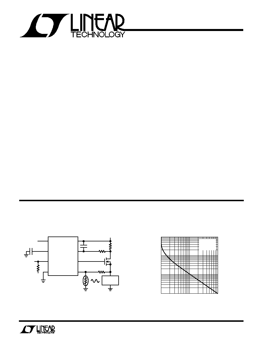
TYPICAL
Trip Delay Time
5V/1A Electronic Circuit Breaker with 1ms Trip Delay,
200ms Auto-Reset Period and 70
°
C Thermal Shutdown
CIRCUIT BREAKER CURRENT (A)
1
0.01
TRIP DELAY (ms)
10
10
100
LTC1153 · TA02
1
0.1
R
SEN
= 0.1
R
D
= 100k
C
D
= 0.01
µ
F
IN
C
T
STATUS
GND
VS
DS
G
SHUTDOWN
LTC1153
C
D
0.01
µ
F
R
D
100k
*R
SEN
0.1
IRLR024
51k
SENSITIVE
5V LOAD
**70°C
PTC
51k
5V
TO
µ
P
C
T
0.22
µ
F
ON/OFF
ALL COMPONENTS SHOWN ARE SURFACE MOUNT.
IMS026 INTERNATIONAL MANUFACTURING SERVICE, INC. (401) 683-9700
RL2006-100-70-30-PT1 KEYSTONE CARBON COMPANY (814) 781-1591
*
**
LTC1153 · TA01
Z5U
2
LTC1153
LTC1153C
SYMBOL
PARAMETER
CONDITIONS
MIN
TYP
MAX
UNITS
V
S
Supply Voltage
q
4.5
18
V
I
Q
Quiescent Current OFF
V
S
= 5V, V
IN
= 0V
8
20
µ
A
I
Q
Quiescent Current ON
V
S
= 5V, V
IN
= 5V
85
120
µ
A
I
Q
Quiescent Current ON
V
S
=12V, V
IN
= 5V
180
400
µ
A
V
INH
Input High Voltage
q
2
V
V
INL
Input Low Voltage
q
0.8
V
I
IN
Input Current
0
V
< V
IN
< V
S
q
±
1
µ
A
C
IN
Input Capacitance
5
pF
V
CT
Timing Capacitor Threshold Voltage
V
S
= 5V
2.1
2.5
2.9
V
V
S
= 12V
2.0
2.6
3.2
V
I
CT
Timing Capacitor Current
V
S
= 12V
3.0
4.2
6.0
µ
A
V
SDH
Shutdown Input High Voltage
q
2
V
V
SDL
Shutdown Input Low Voltage
q
0.8
V
I
SD
Shutdown Input Current
0V < V
IN
< V
S
q
±
1
µ
A
V
SEN
Drain Sense Threshold Voltage
80
100
120
mV
q
75
100
125
mV
I
SEN
Drain Sense Input Current
0V < V
SEN
< V
S
q
±
0.1
µ
A
A
U
G
W
A
W
U
W
A
R
BSOLUTE
XI
TI
S
Supply Voltage ........................................................ 22V
Input Voltage ..................... (V
S
+ 0.3V) to (GND 0.3V)
Timing Capacitor Voltage ... (VS + 0.3V) to (GND 0.3V)
Gate Voltage ....................... (VS + 24V) to (GND 0.3V)
Status Output Voltage .............................................. 15V
Current (Any Pin) .................................................. 50mA
Operating Temperature
LTC1153C .............................................. 0
°
C to 70
°
C
Storage Temperature Range ................. 65
°
c to 150
°
C
Lead Temperature (Soldering, 10 sec.)................ 300
°
C
ELECTRICAL CHARACTERISTICS
V
S
= 4.5V to 18V, T
A
= 25
°
C, C
T
= 0.1
µ
F, V
SD
= 0V unless otherwise noted.
W
U
U
PACKAGE/ORDER I FOR ATIO
ORDER PART
NUMBER
S8 PART MARKING
ORDER PART
NUMBER
LTC1153CN8
T
JMAX
= 100
°
C,
JA
= 150
°
C/W
LTC1153CS8
1153
T
JMAX
= 100
°
C,
JA
= 130
°
C/W (N8)
1
2
3
4
8
7
6
5
TOP VIEW
IN
TIMING CAP
STATUS
GND
V
S
DRAIN SENSE
GATE
SHUTDOWN
N8 PACKAGE
8-LEAD PLASTIC DIP
LTC1153 · PO01
1
2
3
4
8
7
6
5
TOP VIEW
V
S
DRAIN SENSE
GATE
SHUTDOWN
TIMING CAP
STATUS
GND
S8 PACKAGE
8-LEAD PLASTIC SOIC
IN
LTC1154 · PO02
3
LTC1153
LTC1153C
SYMBOL
PARAMETER
CONDITIONS
MIN
TYP
MAX
UNITS
V
GATE
V
S
Gate Voltage Above Supply
V
S
= 5V
q
6.0
7.0
9.0
V
V
S
= 6V
q
7.5
8.3
15.0
V
V
S
= 12V
q
15.0
18.0
25.0
V
V
STAT
Status Output Low Voltage
I
STAT
= 400
µ
A
q
0.05
0.4
V
I
STAT
Status Output Leakage Current
V
STAT
= 12V
q
1
µ
A
t
ON
Turn-ON Time
V
S
= 5V, C
GATE
= 1000pF
Time for V
GATE
> V
S
+ 2V
30
110
300
µ
s
Time for V
GATE
> V
S
+ 5V
100
450
1000
µ
s
V
S
= 12V, C
GATE
= 1000pF
Time for V
GATE
> V
S
+ 5V
20
80
200
µ
s
Time for V
GATE
> V
S
+ 10V
50
160
500
µ
s
t
OFF
Turn-OFF Time
V
S
= 5V, C
GATE
= 1000pF
Time for V
GATE
< 1V
10
36
60
µ
s
V
S
= 12V, C
GATE
= 1000pF
Time for V
GATE
< 1V
10
28
60
µ
s
t
TD
Minimum Trip Delay
V
S
= 5V, C
GATE
= 1000pF
Time for V
GATE
< 1V
5
25
40
µ
s
V
S
= 12V, C
GATE
= 1000pF
Time for V
GATE
< 1V
5
23
40
µ
s
t
SD
Shutdown Turn-OFF Time
V
S
= 5V, C
GATE
= 1000pF
Time for V
GATE
< 1V
17
40
µ
s
V
S
= 12V, C
GATE
= 1000pF
Time for V
GATE
< 1V
13
35
µ
s
ELECTRICAL CHARACTERISTICS
V
S
= 4.5V to 18V, T
A
= 25
°
C, C
T
= 0.1
µ
F, V
SD
= 0V unless otherwise noted.
The
q
denotes specifications which apply over the operating temperature range.
C
C
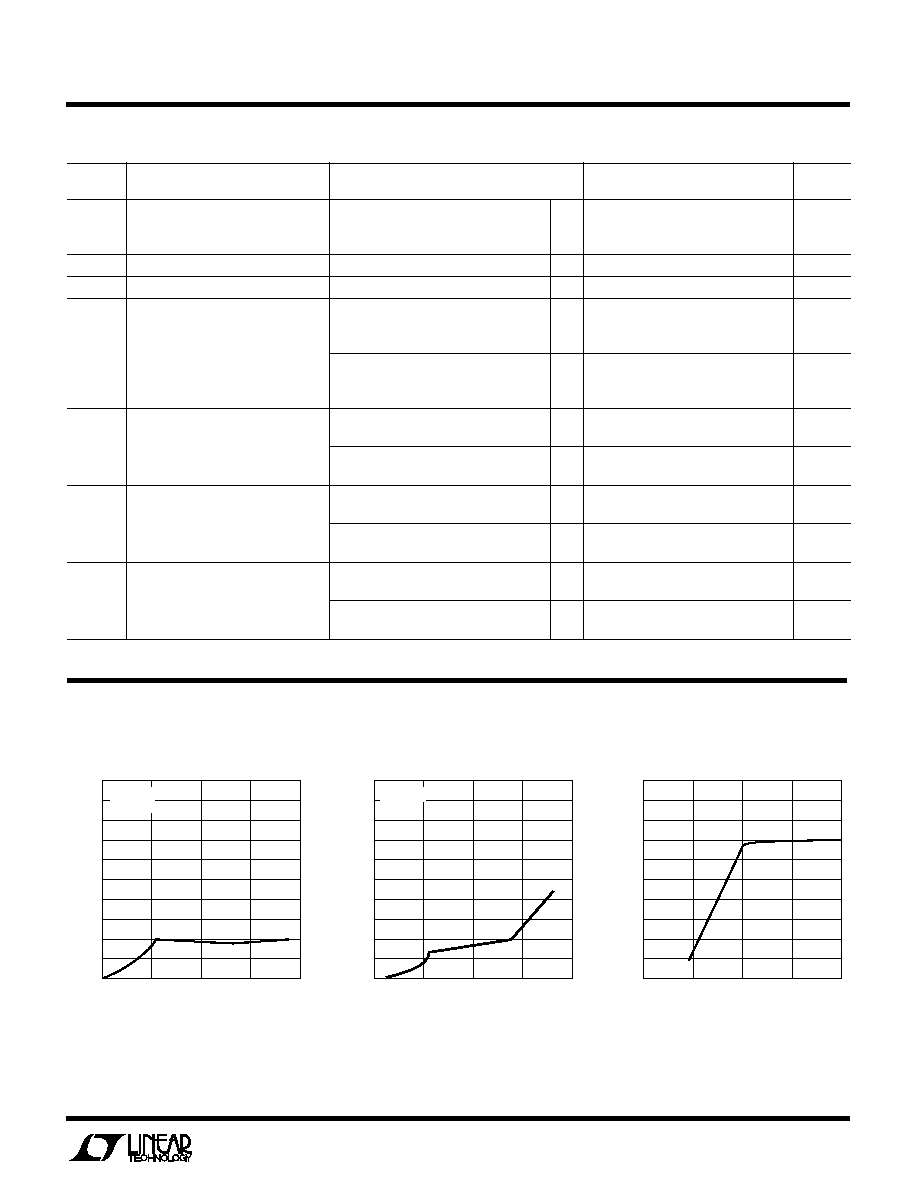
HARA TERISTICS
U
W
A
TYPICAL PERFOR
CE
SUPPLY VOLTAGE (V)
0
0
SUPPLY CURRENT (
µ
A)
5
15
20
25
50
35
5
15
LTC1153 · TPC01
10
40
45
30
10
20
V
IN
= 0V
T
A
= 25°C
Standby Supply Current
Supply Current ON
SUPPLY VOLTAGE (V)
0
4
V
GATE
V
S
(V)
6
10
12
14
24
18
5
10
LTC1153 · TPC03
8
20
22
16
15
20
MOSFET Switch Gate Voltage
SUPPLY VOLTAGE (V)
0
0
SUPPLY CURRENT (
µ
A)
100
300
400
500
1000
700
5
10
LTC1153 · TPC02
200
800
900
600
15
20
T
A
= 25°C
4
LTC1153
C
C
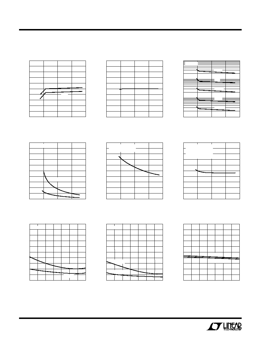
HARA TERISTICS
U
W
A
TYPICAL PERFOR
CE
Input Threshold Voltage
Drain Sense Threshold Voltage
Auto-Reset Period
Supply Current ON
Input ON Threshold Voltage
SUPPLY VOLTAGE (V)
0
0.4
INPUT THRESHOLD VOLTAGE (V)
0.6
1.0
1.2
1.4
2.4
1.8
5
10
LTC1153 · TPC04
0.8
2.0
2.2
1.6
15
20
V
ON
V
OFF
MOSFET Gate Turn-OFF Time
Built-In Trip Delay
Standby Supply Current
TEMPERATURE (°C)
50
0
SUPPLY CURRENT (
µ
A)
5
15
20
25
50
35
0
50
75
LTC1153 · TPC10
10
40
45
30
25
25
100
125
V
IN
= 0V
V
S
= 18V
V
S
= 5V
TEMPERATURE (°C)
50
0
SUPPLY CURRENT (
µ
A)
100
300
400
500
1000
700
0
50
75
LTC1153 · TPC11
200
800
900
600
25
25
100
125
V
IN
= 5V
V
S
= 12V
V
S
= 5V
TEMPERATURE (°C)
50
0.4
INPUT THRESHOLD VOLTAGE (V)
0.6
1.O
1.2
1.4
2.4
1.8
0
50
75
LTC1153 · TPC12
0.8
2.0
2.2
1.6
25
25
100
125
V
S
= 18V
V
S
= 5V
SUPPLY VOLTAGE (V)
0
50
DRAIN SENSE THRESHOLD VOLTAGE (mV)
60
80
90
100
150
120
5
10
LTC1153 · TPC05
70
130
140
110
15
20
SUPPLY VOLTAGE (V)
0
0.01
RESET PERIOD (SEC)
1
10
5
10
20
LTC1153 · TPC06
0.1
15
T
A
= 25°C
3.3
µ
F
1
µ
F
0.1
µ
F
0.033
µ
F
0.33
µ
F
MOSFET Gate Turn-ON Time
SUPPLY VOLTAGE (V)
0
0
TURN ON TIME (
µ
s)
100
300
400
500
1000
700
5
10
LTC1153 · TPC07
200
800
900
600
15
20
V
GS
= 5V
V
GS
= 2V
C
GATE
= 1000pF
SUPPLY VOLTAGE (V)
0
0
TRIP TIME (
µ
s)
5
15
20
25
50
35
5
15
LTC1153 · TPC09
10
40
45
30
10
20
C
GATE
= 1000pF
TIME FOR V
GATE
< 1V
V
SEN
= V
S
1V
NO EXTERNAL DELAY
SUPPLY VOLTAGE (V)
0
0
TURN OFF TIME (
µ
s)
5
15
20
25
50
35
5
15
LTC1153 · TPC08
10
40
45
30
10
20
C
GATE
= 1000pF
TIME FOR V
GATE
< 1V
5
LTC1153
Auto-Reset Time*
Shutdown Threshold Voltage
MOSFET Gate Drive Current
C
C
HARA TERISTICS
U
W
A
TYPICAL PERFOR
CE
TEMPERATURE (°C)
50
0.4
SHUTDOWN THRESHOLD VOLTAGE (V) 0.6
1.O
1.2
1.4
2.4
1.8
0
50
75
LTC1153 · TPC13
0.8
2.0
2.2
1.6
25
25
100
125
V
S
= 18V
V
S
= 5V
TEMPERATURE (°C)
25
0.1
1
10
25
LTC1153 · TPC14
AUTO-RESET TIME (s/
µ
F)
50
125
0
50
75
100
*SECONDS OF DELAY
PER
µ
F C
T
V
S
= 5V
V
S
= 12V
V
S
= 18V
PI FU CTIO S
U
U
U
Input and Shutdown Pins
The LTC1153 input pin is active high and activates all of the
protection and charge pump circuitry when switched ON.
The shutdown pin is designed to break the circuit if a
secondary fault condition (over temperature, etc.) is de-
tected. The LTC1153 logic and shutdown inputs are high
impedance CMOS gates with ESD protection diodes to
ground and supply and therefore should not be forced
beyond the power supply rails. The shutdown pin should
be connected to ground when not in use.
Timing Capacitor Pin (Auto-Reset Timer)
The small capacitor charging current (4.2
µ
A) produces
large delays with relatively small valued capacitors, but
care must be taken to ensure that this current is not
shunted to ground through a leaky capacitor or printed
circuit board trace. The timing capacitor voltage is sensed
by a high impedance CMOS comparator input with ESD
clamp diodes to ground and supply and therefore should
not be forced beyond the power supply rails. This pin can
be grounded if the auto-reset function is not used.
MOSFET Gate Drive Pin
The MOSFET gate drive pin is either driven to ground when
the switch is turned OFF or driven above the supply rail
when the switch is turned ON. This pin is a relatively high
impedance when driven above the rail (the equivalent of a
few hundred k
). Care should be taken to minimize any
loading of this pin by parasitic resistance to ground or
supply.
Supply Pin
The supply pin of the LTC1153 serves two vital purposes.
The first is obvious: it powers the input, gate drive, regu-
lation and protection circuitry. The second purpose is less
obvious: it provides a Kelvin connection to the top of the
drain sense resistor for the internal 100mV reference.
The LTC1153 is designed to be
continuously powered so
that the gate of the MOSFET is actively driven at all times.
If it is necessary to remove power from the supply pin and
then re-apply it, the input pin (or enable pin) should be
cycled a few milliseconds
after the power is re-applied to
reset the input latch and protection circuitry. Also, the
input and enable pins should be isolated with 10k resistors
to limit the current flowing through the ESD protection
diodes to the supply pin.
The supply pin of the LTC1153 should never be forced
below ground as this may result in permanent damage to
the device. A 300
resistor should be inserted in series
with the ground pin if negative supply voltage transients
are anticipated.
GATE VOLTAGE ABOVE SUPPLY (V)
1
GATE DRIVE CURRENT (
µ
A)
10
100
1000
0
8
12
16
0.1
4
20
LTC1153 · TPC15
V
S
= 18V
T
A
= 25°C
V
S
= 12V
V
S
= 5V