 | ÐлекÑÑоннÑй компоненÑ: LTC1069-7 | СкаÑаÑÑ:  PDF PDF  ZIP ZIP |
Äîêóìåíòàöèÿ è îïèñàíèÿ www.docs.chipfind.ru
1
LTC1069-7
Linear Phase
8th Order Lowpass Filter
FEATURES
s
8th Order, Linear Phase Filter in SO-8 Package
s
Raised Cosine Amplitude Response
s
43dB Attenuation at 2
×
f
CUTOFF
s
Wideband Noise: 140
µ
V
RMS
s
Operates from Single 5V Supply to
±
5V Power Supplies
s
Clock-Tunable to 200kHz with
±
5V Supplies
s
Clock-Tunable to 120kHz with Single 5V Supply
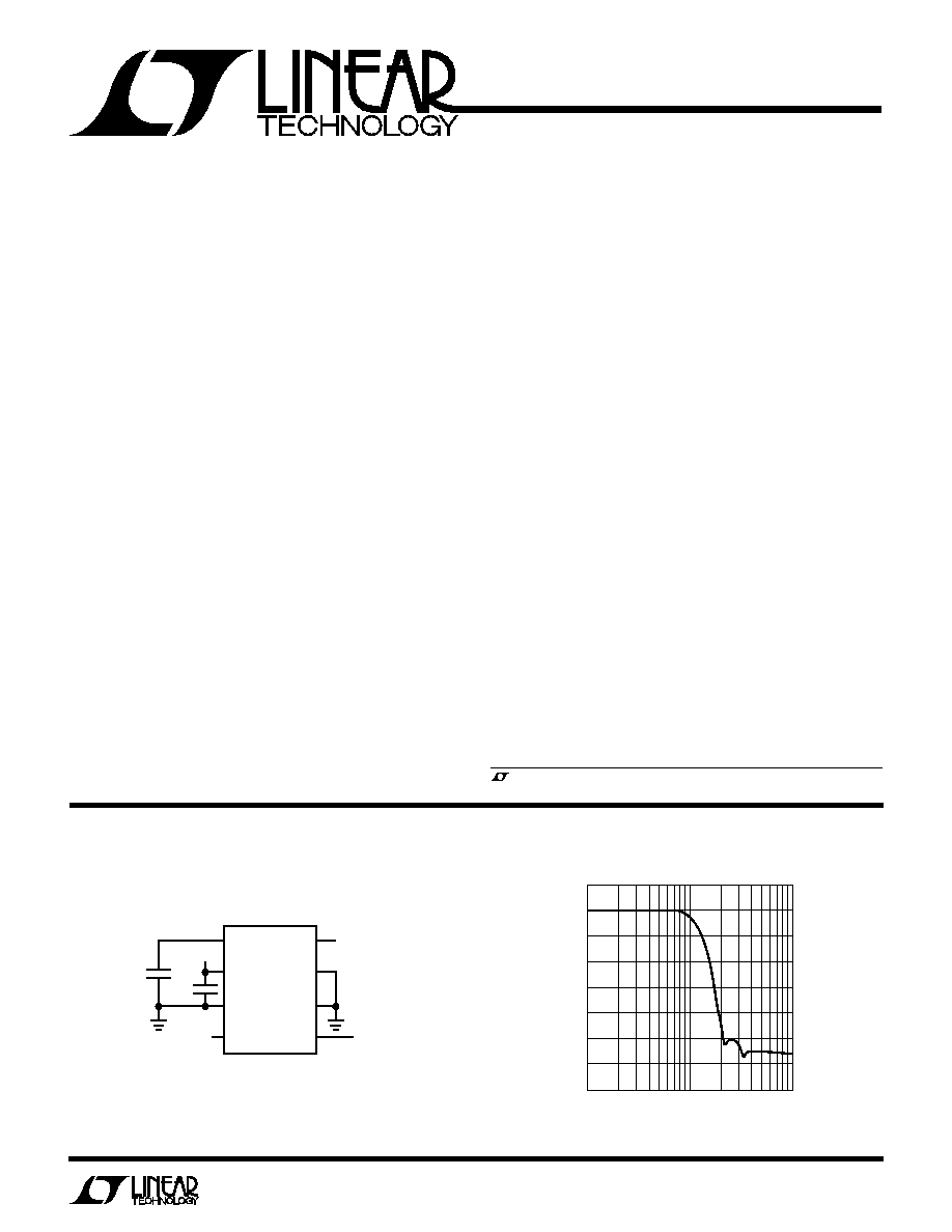
cutoff frequency of the LTC1069-7 is set by an external
clock and is equal to the clock frequency divided by 25.
The ratio of the internal sampling frequency to the cutoff
frequency is 50:1 that is, the input signal is sampled twice
per clock cycle to lower the risk of aliasing. The LTC1069-
7 can be operated from a single 5V supply up to dual
±
5V
supplies.
The gain and phase response of the LTC1069-7 can be
used in digital communication systems where pulse shap-
ing and channel bandwidth limiting must be carried out.
Any system that requires an analog filter with linear phase
and sharper roll off than conventional Bessel filters can
use the LTC1069-7.
The LTC1069-7 has a wide dynamic range. With
±
5V
supplies and an input range of 0.1V
RMS
to 2V
RMS
, the
signal-to-(noise + THD) ratio is
60dB. The wideband
noise of the LTC1069-7 is 140
µ
V
RMS
.
Unlike other
LTC1069-X filters, the typical passband gain of the
LTC1069-7 is equal to 1V/V.
The LTC1069-7 is available in an SO-8 package.
Other filter responses with lower power/speed specifica-
tions can be obtained. Please contact LTC Marketing.
AGND
V
+
NC
V
IN
V
IN
V
OUT
V
OUT
V
NC
CLK
LTC1069-7
f
CLK
= 2.5MHz
5V
0.47
µ
F
0.1
µ
F
1069-7 TA01
Frequency Response
Single 5V Supply, Linear Phase 100kHz Lowpass Filter
The LTC
®
1069-7 is a monolithic, clock-tunable, linear
phase, 8th order lowpass filter. The amplitude response
of the filter approximates a raised cosine filter with an
alpha of one. The gain at the cutoff frequency is 3dB and
the attenuation at twice the cutoff frequency is 43dB. The
DESCRIPTIO
N
U
s
Digital Communication Filter
s
Antialiasing Filter with Linear Phase
s
Smoothing Filters
APPLICATIO
N
S
U
, LTC and LT are registered trademarks of Linear Technology Corporation.
TYPICAL APPLICATIO
N
U
FREQUENCY (kHz)
10
70
GAIN (dB)
60
50
40
30
10
100
1000
1069-7 TA02
20
10
0
2
LTC1069-7
ABSOLUTE
M
AXI
M
U
M
RATINGS
W
W
W
U
PACKAGE/ORDER I
N
FOR
M
ATIO
N
W
U
U
Total Supply Voltage (V
+
to V
) ............................. 12V
Power Dissipation ............................................. 400mW
Operating Temperature Range
LTC1069-7C ........................................... 0
°
C to 70
°
C
LTC1069-7I ....................................... 40
°
C to 85
°
C
Storage Temperature ............................ 65
°
C to 150
°
C
Lead Temperature (Soldering, 10 sec).................. 300
°
C
LTC1069-7CS8
LTC1069-7IS8
ORDER PART
NUMBER
Consult factory for Military grade parts.
ELECTRICAL CHARACTERISTICS
f
CUTOFF
is the filter's cutoff frequency and is equal to f
CLK
/25. The f
CLK
signal level is TTL or CMOS (max clock rise or
fall time
1
µ
s), R
L
= 10k, T
A
= 25
°
C, unless otherwise specified. All AC gains are measured relative to the passband gain.
PARAMETER
CONDITIONS
MIN
TYP
MAX
UNITS
Passband Gain (f
IN
0.2f
CUTOFF
)
V
S
=
±
5V, f
CLK
= 2.5MHz
0.10
±
0.75
dB
f
TEST
= 1kHz, V
IN
= 1V
RMS
q
±
0.90
dB
V
S
= 4.75V, f
CLK
= 500kHz
0.10
±
0.75
dB
f
TEST
= 1kHz, V
IN
= 0.5V
RMS
q
±
0.90
dB
Gain at 0.25f
CUTOFF
V
S
=
±
5V, f
CLK
= 2.5MHz
0.30
dB
f
TEST
= 25kHz, V
IN
= 1V
RMS
q
0.55
0.1
dB
V
S
= 4.75V, f
CLK
= 500kHz
0.05
dB
f
TEST
= 5kHz, V
IN
= 0.5V
RMS
q
0.30
0.15
dB
Gain at 0.50f
CUTOFF
V
S
=
±
5V, f
CLK
= 2.5MHz
1.0
dB
f
TEST
= 50kHz, V
IN
= 1V
RMS
q
1.40
0.35
dB
V
S
= 4.75V, f
CLK
= 500kHz
0.30
dB
f
TEST
= 10kHz, V
IN
= 0.5V
RMS
q
0.60
0
dB
Gain at 0.75f
CUTOFF
V
S
=
±
5V, f
CLK
= 2.5MHz
1.65
dB
f
TEST
= 75kHz, V
IN
= 1V
RMS
q
2.1
0.80
dB
V
S
= 4.75V, f
CLK
= 500kHz
0.75
dB
f
TEST
= 15kHz, V
IN
= 0.5V
RMS
q
1.15
0.25
dB
Gain at f
CUTOFF
V
S
=
±
5V, f
CLK
= 2.5MHz
3.5
dB
f
TEST
= 100kHz, V
IN
= 1V
RMS
q
4.0
2.7
dB
V
S
= 4.75V, f
CLK
= 500kHz
2.9
dB
f
TEST
= 20kHz, V
IN
= 0.5V
RMS
q
3.3
2.4
dB
Gain at 1.5f
CUTOFF
V
S
=
±
5V, f
CLK
= 2.5MHz
16.5
dB
f
TEST
= 150kHz, V
IN
= 1V
RMS
q
19
14
dB
V
S
= 4.75V, f
CLK
= 500kHz
18.1
dB
f
TEST
= 30kHz, V
IN
= 0.5V
RMS
q
20
17
dB
Gain at 2.0f
CUTOFF
V
S
=
±
5V, f
CLK
= 2.5MHz
43
dB
f
TEST
= 200kHz, V
IN
= 1V
RMS
q
55
38
dB
V
S
= 4.75V, f
CLK
= 500kHz
41
dB
f
TEST
= 40kHz, V
IN
= 0.5V
RMS
q
48
39
dB
S8 PART MARKING
10697
10697I
T
JMAX
= 125
°
C,
JA
= 110
°
C/ W
1
2
3
4
8
7
6
5
TOP VIEW
V
OUT
V
NC
CLK
AGND
V
+
NC
V
IN
S8 PACKAGE
8-LEAD PLASTIC SO
3
LTC1069-7
ELECTRICAL CHARACTERISTICS
f
CUTOFF
is the filter's cutoff frequency and is equal to f
CLK
/25. The f
CLK
signal level is TTL or CMOS (max clock rise or
fall time
1
µ
s), R
L
= 10k, T
A
= 25
°
C, unless otherwise specified. All AC gains are measured relative to the passband gain.
PARAMETER
CONDITIONS
MIN
TYP
MAX
UNITS
Gain at 5.0f
CUTOFF
V
S
= 4.75V, f
CLK
= 500kHz
70
59
55
dB
f
TEST
= 100kHz, V
IN
= 0.5V
RMS
Gain at f
CUTOFF
(160kHz)
V
S
=
±
5V, f
CLK
= 4MHz
2.1
dB
f
TEST
= 160kHz, V
IN
= 1V
RMS
Phase at 0.5f
CUTOFF
V
S
=
±
5V, f
CLK
= 2.5MHz
35
30.5
25
Deg
f
TEST
= 50kHz
Phase at f
CUTOFF
V
S
=
±
5V, f
CLK
= 2.5MHz
240
235
230
Deg
f
TEST
= 100kHz
Passband Phase Deviation from
V
S
=
±
5V, f
CLK
= 500kHz
3.0
Deg
Linear Phase (Note 1)
Output DC Offset (Input at GND)
V
S
=
±
5V, f
CLK
= 500kHz
50
mV
V
S
= 4.75V, f
CLK
= 400kHz
25
125
mV
Output Voltage Swing
V
S
=
±
5V, I
SOURCE
/I
SINK
1mA, R
L
= 10k
q
±
3.5
±
4.0
V
V
S
= 4.75V, I
SOURCE
/I
SINK
1mA, R
L
= 10k
q
2.6
3.6
V
P-P
Power Supply Current
V
S
=
±
5V, f
CLK
= 500kHz
18
26
mA
q
29
mA
V
S
= 4.75V, f
CLK
= 400kHz
13
15
mA
q
16.5
mA
The
q
denotes specifications which apply over the full operating
temperature range.
Note 1: Phase Deviation = 1/2(Phase at 0Hz Phase at f
CUTOFF
) (Phase
at 0Hz Phase at 0.5f
CUTOFF
)
Phase at 0Hz = 180
°
(guaranteed by design)
Example: An LTC1069-7 has Phase at 0.5f
CUTOFF
= 30.5
°
and Phase at
f
CUTOFF
= 235
°
.
Passband Phase Deviation from Linear Phase
= 1/2[180
°
( 235
°
)] [(180
°
( 30.5
°
)] = 3
°
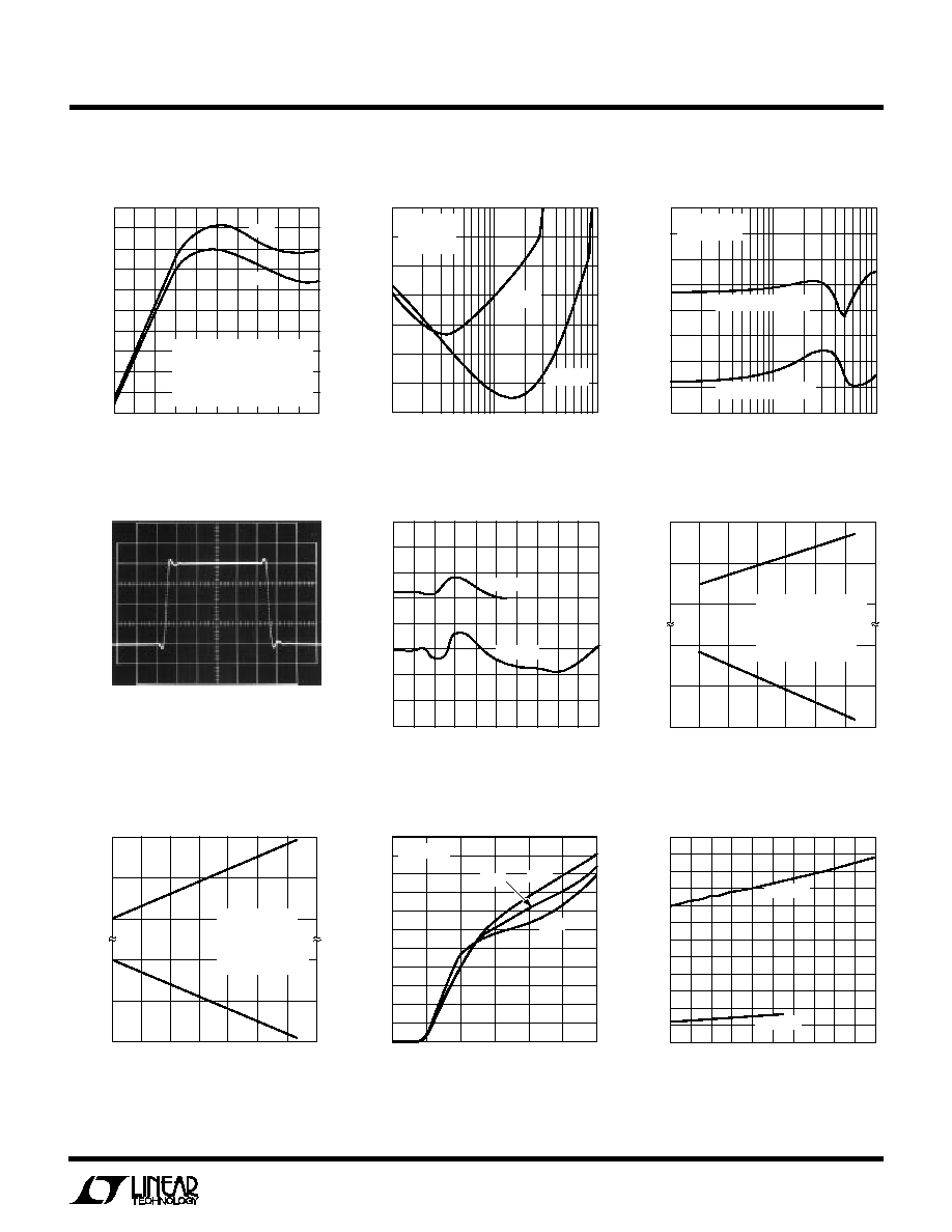
TYPICAL PERFOR
M
A
N
CE CHARACTERISTICS
U
W
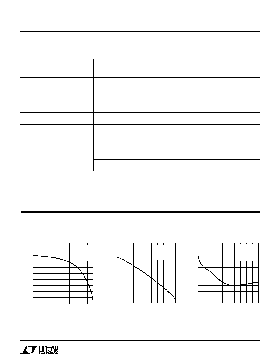
Passband Gain vs Frequency
FREQUENCY (kHz)
1
GAIN (dB)
1.0
0.5
0
0.5
1.0
1.5
2.0
2.5
3.0
3.5
4.0
17
LTC1069-7 · TPC01
5
3
7
11
15
19
9
13
21
V
S
=
±
5V
f
CLK
= 500kHz
f
C
= 20kHz
V
IN
= 2V
RMS
FREQUENCY (kHz)
41
GAIN (dB)
40
42
44
46
48
50
52
54
56
58
60
73
LTC1069-7 · TPC03
49
45
53
61
69
77
57
65
81
V
S
=
±
5V
f
CLK
= 500kHz
f
C
= 20kHz
V
IN
= 2V
RMS
Stopband Gain vs Frequency
FREQUENCY (kHz)
GAIN (dB)
10
0
10
20
30
40
50
25
29
33
37
LTC1069-7 · TPC02
41
23
21
27
31
35
39
V
S
=
±
5V
f
CLK
= 500kHz
f
C
= 20kHz
V
IN
= 2V
RMS
Transition Band Gain vs Frequency
4
LTC1069-7
TYPICAL PERFOR
M
A
N
CE CHARACTERISTICS
U
W
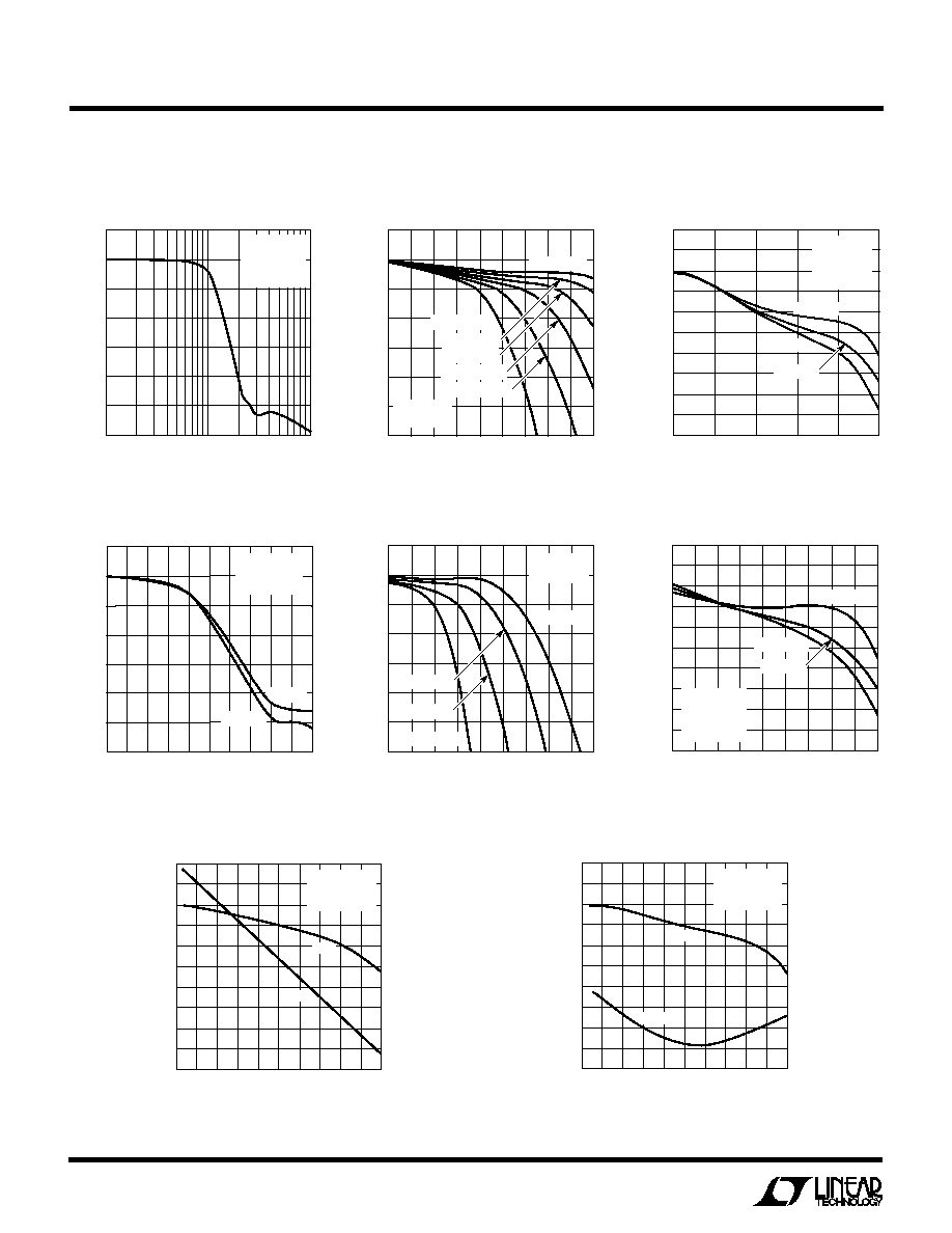
Passband Gain vs
Clock Frequency
FREQUENCY (kHz)
20
GAIN (dB)
100
3
0
3
6
9
12
15
18
LTC1069-7 · TPC05
60
140
40
120
80
160 180 200
f
CLK
= 2.5MHz
f
CLK
= 3.5MHz
f
CLK
= 3MHz
f
CLK
= 4MHz
f
CLK
= 4.5MHz
f
CLK
= 5MHz
V
S
=
±
5V
V
IN
= 2V
RMS
Gain vs Frequency
FREQUENCY (kHz)
1
GAIN (dB)
10
0
10
20
30
40
50
60
10
100
LTC1069-7 · TPC04
V
S
=
±
5V
f
CLK
= 250kHz
f
C
= 10kHz
V
IN
= 1V
RMS
FREQUENCY (kHz)
10
GAIN (dB)
1.0
0.5
0
0.5
1.0
1.5
2.0
2.5
3.0
3.5
4.0
130
LTC1069-7 · TPC06
40
70
100
160
T
A
= 85
°
C
T
A
= 40
°
C
T
A
= 25
°
C
V
S
=
±
5V
f
CLK
= 4MHz
f
C
= 160kHz
V
IN
= 2V
RMS
Passband Gain vs Frequency
Passband Gain vs
Clock Frequency
Gain vs Supply Voltage
Passband Gain vs Frequency
FREQUENCY (kHz)
10
GAIN (dB)
10
0
10
20
30
40
50
60
30
110
150
LTC1069-7 · TPC07
90
190 210
50 70
130
170
V
S
= 5V
V
S
=
±
5V
f
CLK
= 2MHz
f
C
= 80kHz
V
IN
= 0.5V
RMS
FREQUENCY (kHz)
20
GAIN (dB)
100
3
0
3
6
9
12
15
18
LTC1069-7 · TPC08
60
140
40
120
80
160 180 200
f
CLK
= 1.5MHz
f
CLK
= 2MHz
f
CLK
= 2.5MHz
f
CLK
= 3MHz
V
S
= 5V
V
IN
= 1V
RMS
FREQUENCY (kHz)
10
GAIN (dB)
1.0
0.5
0
0.5
1.0
1.5
2.0
2.5
3.0
3.5
4.0
30
50
60
100
LTC1069-7 · TPC09
20
40
70
80
90
T
A
= 85
°
C
T
A
= 40
°
C
T
A
= 25
°
C
V
S
= 5V
f
CLK
= 2.5MHz
f
C
= 100kHz
V
IN
= 1V
RMS
Passband Gain and Phase vs
Frequency
FREQUENCY (kHz)
0
GAIN (dB)
PHASE (DEG)
2
1
0
1
2
3
4
5
6
7
8
180
135
90
45
0
45
90
135
180
225
270
80
LTC1069-7 · TPC10
20
10
30
50
70
90
40
60
100
GAIN
PHASE
V
S
=
±
5V
f
CLK
= 2.5MHz
f
C
= 100kHz
Passband Gain and Delay vs
Frequency
FREQUENCY (kHz)
0
GAIN (dB)
DELAY (
µ
s)
2
1
0
1
2
3
4
5
6
7
8
13.5
13.0
12.5
12.0
11.5
11.0
80
LTC1069-7 · TPC12
20
10
30
50
70
90
40
60
100
GAIN
DELAY
V
S
=
±
5V
f
CLK
= 2.5MHz
f
C
= 100kHz
5
LTC1069-7
TYPICAL PERFOR
M
A
N
CE CHARACTERISTICS
U
W
Phase Matching vs Frequency
FREQUENCY (f
CUTOFF
/FREQUENCY)
0
PHASE DIFFERENCE (DEG)
2.50
2.25
2.00
1.75
1.50
1.25
1.00
0.75
0.50
0.25
0
0.8
LTC1069-7 · TPC11
0.2
0.1
0.3
0.5
0.7
0.9
0.4
0.6
1.0
70
°
C
25
°
C
V
S
=
±
5V
f
CLK
2.5MHz
PHASE DIFFERENCE BETWEEN
ANY TWO UNITS (SAMPLE OF
20 REPRESENTATIVE UNITS)
THD + Noise vs Frequency
THD + Noise vs Input (V
P-P
)
INPUT (V
P-P
)
0.1
THD + NOISE (dB)
40
45
50
55
60
65
70
75
1
10
LTC1609-7 · TPC13
V
S
=
±
5V
V
S
= 5V
f
CLK
= 1MHz
f
C
= 40kHz
f
IN
= 1kHz
FREQUENCY (kHz)
1
THD + NOISE (dB)
40
45
50
55
60
65
70
75
80
10
100
LTC1069-7 · TPC14
f
CLK
= 2.5MHz
f
C
= 100kHz
V
S
= 5V, V
IN
= 1V
P-P
V
S
=
±
5V, V
IN
= 2V
P-P
Transient Response
Output Voltage Swing vs
Temperature
Output Offset vs Clock Frequency
CLOCK FREQUENCY (MHz)
0.25
OUTPUT OFFSET (mV)
10
15
20
25
30
35
40
45
50
4.25
LTC1069-7 · TPC16
1.25
2.25
3.25
5.25
V
S
= 5V
V
S
=
±
5V
Output Voltage Swing vs
Temperature
Supply Current vs
Clock Frequency
Supply Current vs
Supply Voltage
SUPPLY VOLTAGE (
±
V)
0
SUPPLY CURRENT (mA)
1
2
LTC1069-7 · TPC19
3
6
25
20
15
10
5
0
4
5
85
°
C
40
°
C
25
°
C
f
CLK
= 10Hz
CLOCK FREQUENCY (MHz)
0.25
1.25
2.25
3.25
4.25
5.25
SUPPLY CURRENT (mA)
LTC1263 · TPC20
22
21
20
19
18
17
16
15
14
13
12
11
10
V
S
=
±
5V
V
S
= 5V
1V/DIV
V
S
=
±
5V
0.1ms/DIV
LTC1069-7 · TPC15
f
CLK
= 500kHz
f
CUTOFF
= 20kHz
V
IN
= 4V
P-P
SQUARE WAVE AT 1kHz
TEMPERATURE (
°
C)
40
1.0
VOLTAGE SWING (V)
1.2
4.3
0
40
60
LTC1069-7 · TPC17
1.1
4.2
4.1
20
20
80
100
V
S
= 5V (AGND AT 2.5V)
f
CLK
= 500kHz
f
CUTOFF
= 20kHz
R
L
= 10k
I
SOURCE
/I
SINK
1mA
TEMPERATURE (
°
C)
40
4.7
VOLTAGE SWING (V)
4.5
4.2
0
40
60
LTC1069-7 · TPC18
4.6
4.1
4.0
20
20
80
100
V
S
=
±
5V
f
CLK
= 2.5MHz
f
CUTOFF
= 100kHz
R
L
= 10k
I
SOURCE
/I
SINK
= 1mA