 | ÐлекÑÑоннÑй компоненÑ: LT5537 | СкаÑаÑÑ:  PDF PDF  ZIP ZIP |
5537f.pm65
1
LT5537
5537f
Linear-to-Log Signal Level Conversion
Received Signal Strength Indication (RSSI)
RF Power Control
RF/IF Power Detection
Receiver RF/IF Gain Control
Envelope Detection
ASK Receiver
Wide Dynamic Range
RF/IF Log Detector
Low Frequency to 1000MHz Operation
83dB Dynamic Range with
±1dB Nonlinearity
at 200MHz
Sensitivity 76dBm or Better at 200MHz
Log-Linear Transfer Slope of 20mV/dB
Supply Voltage Range: 2.7V to 5.25V
Supply Current: 13.5mA at 3V
Tiny 8-Lead (3mm
× 2mm) DFN Package
FEATURES
DESCRIPTIO
U
APPLICATIO S
U
TYPICAL APPLICATIO
U
, LTC and LT are registered trademarks of Linear Technology Corporation.
All other trademarks are the property of their respective owners.
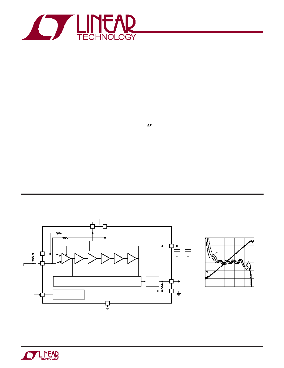
The LT
®
5537 is a wide dynamic range RF/IF detector,
operational from below 10MHz to 1000MHz. The lower
limit of the operating frequency range can be extended to
near DC by the use of an external capacitor. The input
dynamic range at 200MHz with
±3dB nonlinearity is 90dB
(from 76dBm to 14dBm, single-ended 50
input). The
detector output voltage slope is nominally 20mV/dB, and
the typical temperature coefficient is 0.01dB/
°C at 200MHz.
1
OFFSET
CANCELLATION
DETECTOR CELLS
EXPOSED PAD
BANDGAP REFERENCE
AND BIASING
OUTPUT
BUFFER
ENBL
3
IN
2
IN
+
5
CAP
OUT
5537 TA01a
V
EE
OPTIONAL
4
CAP
+
7k
7k
15nF
RF IN
15nF
8
7
9
V
CC
1
µF
6
1nF
7.2k
INPUT POWER (dBm)
80
0
V
OUT
(V)
LINEARITY ERROR (dB)
0.4
0.8
1.2
1.6
2.0
2.4
40
°C
3
2
1
0
1
2
3
60
40
20
0
5537 TA01b
20
85
°C
25
°C
V
CC
= ENBL = 3V
Output Voltage, Linearity Error
vs Input Power at 200MHz
2
LT5537
5537f
(Note 1)
Power Supply Voltage ........................................... 5.5V
Enable Voltage ................................... 0.2V, V
CC
+ 0.2V
Input Power (Note 2) ......................................... 22dBm
Operating Ambient Temperature Range .. 40
°C to 85°C
Storage Temperature Range ................ 65
°C to 125°C
Maximum Junction Temperature ......................... 125
°C
ABSOLUTE AXI U RATI GS
W
W
W
U
Consult LTC Marketing for parts specified with wider operating temperature ranges.
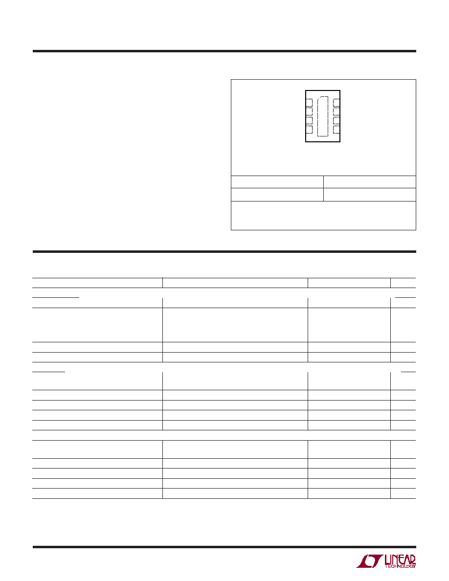
PACKAGE/ORDER I FOR ATIO
U
U
W
LT5537EDDB
ORDER PART NUMBER
DDB PART MARKING
LBJR
JA
= 76
°C/W
EXPOSED PAD (PIN 9) SHOULD BE SOLDERED TO PCB
TOP VIEW
9
DDB PACKAGE
8-LEAD (3mm
´ 2mm) PLASTIC DFN
5
6
7
8
4
3
2
1
ENBL
IN
+
IN
CAP
+
OUT
V
EE
V
CC
CAP
Order Options Tape and Reel: Add #TR
Lead Free: Add #PBF Lead Free Tape and Reel: Add #TRPBF
Lead Free Part Marking:
http://www.linear.com/leadfree/
V
CC
= 3V, ENBL = 3V, T
A
= 25
°C, unless otherwise specified. (Notes 3, 4)
ELECTRICAL CHARACTERISTICS
PARAMETER
CONDITIONS
MIN
TYP
MAX
UNITS
Signal Input
Input Frequency Range
(Note 5)
10 to 1000
MHz
Maximum Input Power for Monotonic Output
50
Termination
200MHz
14.0
dBm
600MHz
11.6
dBm
1GHz
9.4
dBm
DC Common Mode Voltage
V
CC
0.4
V
Small-Signal Impedance
Measured at 200MHz
1.73k
//1.45pF
f = 10MHz
Linear Dynamic Range
±3dB Error
88.8
dB
±1dB Error
72.5
dB
Slope
R1 = 33k (Note 8)
19.6
mV/dB
Intercept
V
OUT
= 0V, Extrapolated
97
dBm
Sensitivity
(Notes 3, 7)
76.7
dBm
Temperature Coefficient
P
IN
= 20dBm
0.007
dB/
°C
f = 50MHz
Linear Dynamic Range
±3dB Error
90.6
dB
±1dB Error
81.0
dB
Slope
R1 = 33k (Note 8)
20
mV/dB
Intercept
V
OUT
= 0V, Extrapolated
96
dBm
Sensitivity
(Notes 3, 7)
77.2
dBm
Temperature Coefficient
P
IN
= 20dBm
0.005
dB/
°C

3
LT5537
5537f
V
CC
= 3V, ENBL = 3V, T
A
= 25
°C, unless otherwise specified. (Notes 3, 4)
ELECTRICAL CHARACTERISTICS
PARAMETER
CONDITIONS
MIN
TYP
MAX
UNITS
f = 100MHz
Linear Dynamic Range
±3dB Error
90.5
dB
±1dB Error
82.8
dB
Slope
R1 = 33k (Note 8)
20.3
mV/dB
Intercept
V
OUT
= 0V, Extrapolated
95
dBm
Sensitivity
(Notes 3, 7)
77
dBm
Temperature Coefficient
P
IN
= 20dBm
0.004
dB/
°C
f = 200MHz
Linear Dynamic Range
±3dB Error
90.3
dB
±1dB Error
83.5
dB
Slope
R1 = 33k (Note 8)
21.2
mV/dB
Intercept
V
OUT
= 0V, Extrapolated
94
dBm
Sensitivity
(Notes 3, 7)
76.4
dBm
Temperature Coefficient
P
IN
= 20dBm
0.010
dB/
°C
f = 400MHz
Linear Dynamic Range
±3dB Error
88.2
dB
±1dB Error
70.8
dB
Slope
R1 = 33k (Note 8)
23.1
mV/dB
Intercept
V
OUT
= 0V, Extrapolated
91
dBm
Sensitivity
(Notes 3, 7)
75.3
dBm
Temperature Coefficient
P
IN
= 20dBm
0.019
dB/
°C
f = 600MHz
Linear Dynamic Range
±3dB Error
85.8
dB
±1dB Error
72.5
dB
Slope
R1 = 33k (Note 8)
25.2
mV/dB
Intercept
V
OUT
= 0V, Extrapolated
89
dBm
Sensitivity
(Notes 3, 7)
74.1
dBm
Temperature Coefficient
P
IN
= 20dBm
0.026
dB/
°C
f = 1GHz
Linear Dynamic Range
±3dB Error
63.5
dB
±1dB Error
51.7
dB
Slope
R1 = 33k (Note 8)
31.4
mV/dB
Intercept
V
OUT
= 0V, Extrapolated
80
dBm
Sensitivity
(Notes 3, 7)
69.2
dBm
Temperature Coefficient
P
IN
= 20dBm
0.031
dB/
°C
Output
Starting Voltage
No RF Signal Present
0.4
V
Response Time
Input from 30dBm to 0dBm, C
LOAD
= 2.5pF
110
ns
Baseband Modulation Bandwidth
Output Load Capacitance = 2.5pF
6
MHz
Shutdown Mode
ENBL = High (On)
1
V
ENBL = Low (Off)
0.3
V
ENBL Input Current
V
ENBL
= 3V
100
µA
V
ENBL
= 0V
0
µA
Turn-On Time
100
µs
Turn-Off Time
100
µs
4
LT5537
5537f
TYPICAL PERFOR A CE CHARACTERISTICS
U
W
Note 1: Absolute Maximum Ratings are those values beyond which the life
of a device may be impaired.
Note 2: Maximum differential AC input voltage between IN
+
and IN
is 4V
peak. Equivalent to 22dBm with 50
input impedance or 16dBm with
200
input impedance (1:4 transformer used).
Note 3: Tests are performed as shown in the configuration of Figure 13.
Note 4: Specifications over the 40
°C to 85°C temperature range are
assured by design, characterization and correlation with statistical process
control.
Note 5: Operation at lower frequency is possible as described in the "Low
Frequency Operation" section in Applications Information.
Note 6: The maximum output voltage is limited to approximately V
CC
0.6V. Either the output slope should be reduced or input power level
should be limited in order to avoid saturating the output circuit when V
CC
<
3V. See discussion in "Dynamic Range" section.
Note 7: Sensitivity is defined as the minimum input power required for the
output voltage to be within 3dB of the ideal log-linear transfer curve.
Sensitivity can be improved by as much as 10dB by using a narrowband
input impedance transformation network. See discussion in "Input
Matching" section.
Note 8: The output slope is adjustable using an external pull-down resistor
(R1). See Applications Information for description of the output circuit.
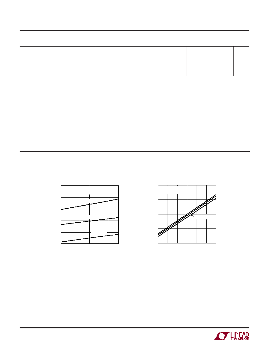
SUPPLY VOLTAGE (V)
2.5
10
SUPPLY CURRENT (mA)
12
14
16
18
20
3.0
3.5
4.0
4.5
5537 G02
5.0
5.5
T
A
= 85
°C
T
A
= 25
°C
T
A
= 40
°C
RF INPUT SIGNAL OFF
ENBL = V
CC
SUPPLY VOLTAGE (V)
2.5
50
ENBL CURRENT (
µ
A)
100
150
200
250
3.0
3.5
4.0
4.5
5537 G03
5.0
5.5
T
A
= 85
°C
T
A
= 40
°C
T
A
= 25
°C
RF INPUT SIGNAL OFF
ENBL = V
CC
Supply Current vs Supply Voltage
ENBL Current vs Supply Voltage
V
CC
= 3V, ENBL = 3V, T
A
= 25
°C, unless otherwise specified. (Notes 3, 4)
ELECTRICAL CHARACTERISTICS
PARAMETER
CONDITIONS
MIN
TYP
MAX
UNITS
Power Supply
Supply Voltage
(Note 6)
2.7
5.25
V
Supply Current
V
CC
= 3V
10
13.5
15
mA
Shutdown Current
ENBL = Low
500
µA
5
LT5537
5537f
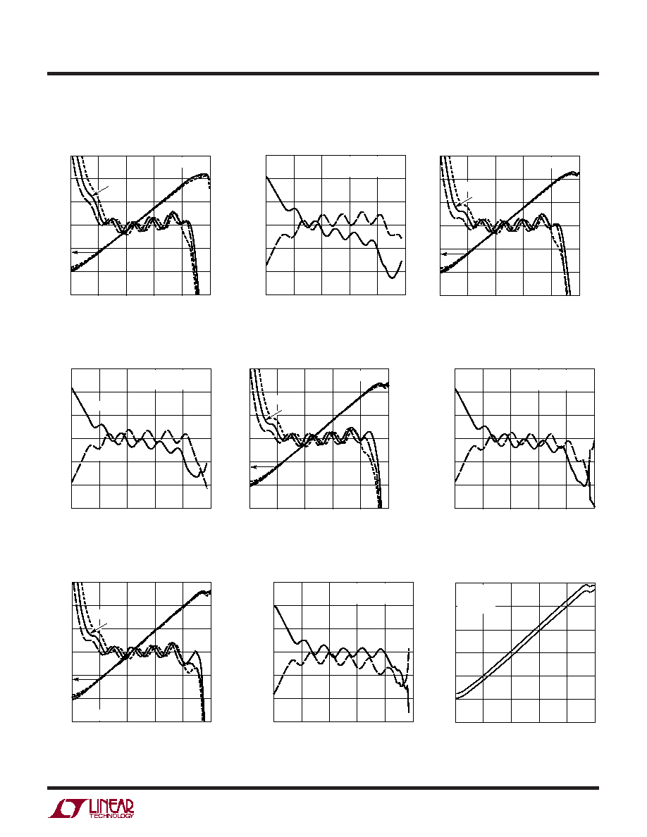
TYPICAL PERFOR A CE CHARACTERISTICS
U
W
V
OUT
Variation vs Input Power
at 50MHz
Output Voltage, Linearity Error
vs Input Power at 100MHz
V
OUT
Variation vs Input Power
at 100MHz
INPUT POWER (dBm)
80
3
V
OUT
VARIATION (dB)
2
1
0
1
2
3
60
40
20
0
5537 G07
20
NORMALIZED AT 25
°C
V
CC
= ENBL = 3V
85
°C
40
°C
INPUT POWER (dBm)
80
0
V
OUT
(V)
LINEARITY ERROR (dB)
0.4
0.8
1.2
1.6
2.0
2.4
40
°C
3
2
1
0
1
2
3
60
40
20
0
5537 G08
20
25
°C
V
CC
= ENBL = 3V
85
°C
INPUT POWER (dBm)
80
3
V
OUT
VARIATION (dB)
2
1
0
1
2
3
60
40
20
0
5537 G09
20
NORMALIZED AT 25
°C
V
CC
= ENBL = 3V
85
°C
40
°C
Output Voltage, Linearity Error
vs Input Power at 200MHz
V
OUT
Variation vs Input Power
at 200MHz
Typical Detector Characteristics
INPUT POWER (dBm)
80
0
V
OUT
(V)
LINEARITY ERROR (dB)
0.4
0.8
1.2
1.6
2.0
2.4
40
°C
3
2
1
0
1
2
3
60
40
20
0
5537 G10
20
85
°C
25
°C
V
CC
= ENBL = 3V
INPUT POWER (dBm)
80
3
V
OUT
VARIATION (dB)
2
1
0
1
2
3
60
40
20
0
5537 G11
20
NORMALIZED AT 25
°C
V
CC
= ENBL = 3V
85
°C
40
°C
INPUT POWER (dBm)
80
V
OUT
(V)
1.6
5V
3V
2.0
2.4
0
5537 G12
1.2
0.8
0.4
0
60
40
20
20
T
A
= 25
°C
200MHz
ENBL = V
CC
Output Voltage, Linearity Error
vs Input Power at 10MHz
V
OUT
Variation vs Input Power
at 10MHz
INPUT POWER (dBm)
80
0
V
OUT
(V)
LINEARITY ERROR (dB)
0.4
0.8
1.2
1.6
2.0
2.4
40
°C
3
2
1
0
1
2
3
60
40
20
0
5537 G04
20
85
°C
25
°C
V
CC
= ENBL = 3V
Output Voltage, Linearity Error
vs Input Power at 50MHz
INPUT POWER (dBm)
80
3
V
OUT
VARIATION (dB)
2
1
0
1
2
3
40
°C
60
40
20
0
5537 G05
20
85
°C
NORMALIZED AT 25
°C
V
CC
= ENBL = 3V
INPUT POWER (dBm)
80
0
V
OUT
(V)
LINEARITY ERROR (dB)
0.4
0.8
1.2
1.6
2.0
2.4
40
°C
3
2
1
0
1
2
3
60
40
20
0
5537 G06
20
25
°C
V
CC
= ENBL = 3V
85
°C