 | ÐлекÑÑоннÑй компоненÑ: LT1331 | СкаÑаÑÑ:  PDF PDF  ZIP ZIP |
Äîêóìåíòàöèÿ è îïèñàíèÿ www.docs.chipfind.ru
1
LT1331
3V RS562 or 5V/3V RS232
Transceiver with One Receiver
Active in Shutdown
S
FEATURE
D
U
ESCRIPTIO
The LT
®
1331 is a 3-driver, 5-receiver RS232 transceiver
designed for 3V and mixed 3V/5V systems. Receivers
operate from 3V logic supply V
L
, while the onboard charge
pump and drivers operate from 5V or 3V supply V
CC
.
The transceiver has two shutdown modes. One mode
disables the drivers and the charge pump, the other shuts
down all circuitry except for one low power receiver which
can be used for ring detection. The V
CC
supply may be shut
down while in ring detection mode. While shut down, the
drivers and receivers assume high impedance output
states.
The LT1331 is fully compliant with all EIA-RS232 specifi-
cations when V
CC
= 5V. If V
CC
= 3V, output drive levels are
compatible with all known interface circuits. Special bipo-
lar construction techniques protect the drivers and receiv-
ers beyond the fault conditions stipulated for RS232. The
RS232 I/O pins are resilient to multiple
±
10kV ESD strikes.
An advanced driver output stage operates up to 120kbaud
while driving heavy capacitive loads.
s
RS232 Compatible 3V Operation
s
3V Logic Interface
s
ESD Protection Over
±
10kV
s
120kbaud Operation for R
L
= 3k, C
L
= 2500pF
s
250kbaud Operation for R
L
= 3k, C
L
= 1000pF
s
One Low Power Receiver Remains Active While
in Shutdown
s
60
µ
A Supply Current in Shutdown
s
Low Power Driver Disable Mode
s
Uses Small Capacitors: 0.1
µ
F, 0.2
µ
F
s
CMOS Comparable Low Power: 60mW
s
Easy PC Layout: Flowthrough Architecture
s
Rugged Bipolar Design
s
Outputs Assume a High Impedance State When
Off or Powered Down
s
Notebook Computers
s
Palmtop Computers
U
S
A
O
PPLICATI
, LTC and LT are registered trademarks of Linear Technology Corporation.
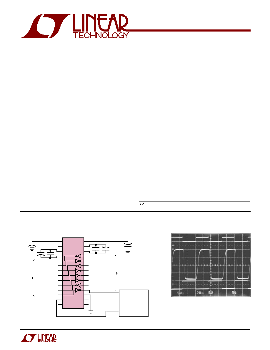
R
1331 TA02
RECEIVER
OUTPUT
C
L
= 50pF
DRIVER
OUTPUT
R
L
= 3k
C
L
= 2500pF
INPUT
U
A
O
PPLICATI
TYPICAL
3.3V Operation
1
2
3
4
5
6
7
8
9
10
11
12
13
14
28
27
26
25
24
23
22
21
20
19
18
17
16
15
DRIVER 1 IN
RX1 OUT
DRIVER 2 IN
RX2 OUT
RX3 OUT
RX4 OUT
DRIVER 3 IN
V
+
0.1
µ
F
2
×
0.1
µ
F
2
×
0.1
µ
F
0.1
µ
F
GND
DRIVER DISABLE
NC
TO LINE
TO LOGIC
V
1331 TA01
RX5 OUT (LOW-Q)
RING DETECT IN
µ
CONTROLLER
OR
µ
PROCESSOR
SHUTDOWN
CONTROL OUT
LT1331
V
CC
= 3.3V
DRIVER 1 OUT
RX1 IN
DRIVER 2 OUT
RX2 IN
RX3 IN
RX4 IN
DRIVER 3 OUT
RX5 IN (LOW-Q)
ON/OFF
3.3V V
L
+
+
+
+
2
LT1331
A
U
G
W
A
W
U
W
A
R
BSOLUTE
XI
TI
S
W
U
U
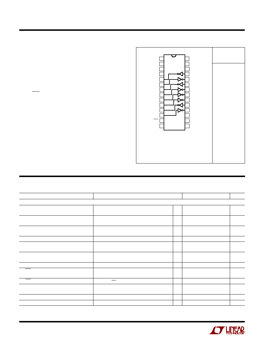
PACKAGE/ORDER I FOR ATIO
ORDER PART
NUMBER
LT1331CG
LT1331CNW
LT1331CSW
1
2
3
4
5
6
7
8
9
10
11
12
13
14
V
+
5V/3V V
CC
C1
+
C1
DRIVER 1 OUT
RX1 IN
DRIVER 2 OUT
RX2 IN
RX3 IN
RX4 IN
DRIVER 3 OUT
ON/OFF
3.3V V
L
28
27
26
25
24
23
22
21
20
19
18
17
16
15
V
C2
C2
+
DRIVER 1 IN
RX1 OUT
DRIVER 2 IN
RX2 OUT
RX3 OUT
RX4 OUT
DRIVER 3 IN
GND
NC
NW PACKAGE
28-LEAD PDIP
TOP VIEW
SW PACKAGE
28-LEAD PLASTIC SO
G PACKAGE
28-LEAD SSOP
RX5 IN
(LOW-Q)
RX5 OUT
(LOW-Q)
DRIVER
DISABLE
Consult factory for Industrial and Military grade parts.
T
JMAX
= 125
°
C,
JA
= 96
°
C/ W (G)
T
JMAX
= 125
°
C,
JA
= 56
°
C/ W (NW)
T
JMAX
= 125
°
C,
JA
= 85
°
C/ W (SW)
PARAMETER
CONDITIONS
MIN
TYP
MAX
UNITS
Power Supply Generator
V
+
Output
V
CC
= 5V
8.6
V
V
CC
= 3.3V
5.5
V
V
Output
V
CC
= 5V
7.0
V
V
CC
= 3.3V
4.8
V
Supply Current (V
CC
)
V
CC
= 5V (Note 3)
q
12
17
mA
V
CC
= 3.3V
q
12
17
mA
Supply Current (V
L
)
(Note 4)
q
3
5
mA
Supply Current When OFF (V
CC
)
Shutdown (Note 5)
q
2
50
µ
A
Driver Disable
0.1
1
mA
Supply Current When OFF (V
L
)
Shutdown (Note 5)
q
60
100
µ
A
Driver Disable
3
5
mA
Supply Rise Time, Shutdown to Turn-On
C1 = C2 = 0.2
µ
F, C
+
= C
= 0.1
µ
F
0.2
ms
ON/OFF Pin Thresholds
Input Low Level (Device Shut Down)
q
1.4
0.8
V
Input High Level (Device Enabled)
q
2.4
1.4
V
ON/OFF Pin Current
0V
V
ON/OFF
5V
q
15
80
µ
A
DRIVER DISABLE Pin Thresholds
Input Low Level (Drivers Enabled)
q
1.4
0.8
V
Input High Level (Drivers Disabled)
q
2.4
1.4
V
DRIVER DISABLE Pin Current
0V
V
DRIVER DISABLE
5V
q
10
500
µ
A
Oscillator Frequency
130
kHz
ELECTRICAL C
C
HARA TERISTICS
(Note 2)
(Note 1)
Supply Voltage (V
CC
) ................................................ 6V
Supply Voltage (V
L
) .................................................. 6V
V
+
........................................................................ 13.2V
V
...................................................................... 13.2V
Input Voltage
Driver ........................................................... V
+
to V
Receiver ................................................ 30V to 30V
ON/OFF ...................................... 0.3V to V
CC
+ 0.3V
DRIVER DISABLE ...................... 0.3V to V
CC
+ 0.3V
Output Voltage
Driver ................................................... 30V to 30V
Receiver ...................................... 0.3V to V
L
+ 0.3V
Short Circuit Duration
V
+
................................................................... 30 sec
V
................................................................... 30 sec
Driver Output .............................................. Indefinite
Receiver Output .......................................... Indefinite
Operating Temperature Range .................... 0
°
C to 70
°
C
Storage Temperature Range ................ 65
°
C to 150
°
C
Lead Temperature (Soldering, 10 sec)................. 300
°
C
3
LT1331
ELECTRICAL C
C
HARA TERISTICS
The
q
denotes specifications which apply over the full operating
temperature range (0
°
C
T
A
70
°
C for commercial grade).
Note 1: Absolute Maximum Ratings are those values beyond which the life
of a device may be impaired.
Note 2: Testing done at V
CC
= 5V, V
L
= 3.3V, and V
ON/OFF
= 3V, unless
otherwise stated.
Note 3: Supply current is measured as the average over several charge
pump cycles. C
+
= 1
µ
F, C
= 0.1
µ
F, C1 = C2 = 0.2
µ
F. All outputs are open
with all driver inputs tied high.
Note 4: V
L
supply current is measured with all receiver outputs high.
Note 5: Supply current and leakage current measurements in shutdown
are performed with V
ON/OFF
0.1V. Supply current measurements using
driver disable are performed with V
DRIVER DISABLE
3V.
Note 6: For driver delay measurements, R
L
= 3k and C
L
= 51pF. Trigger
points are set between the driver's input logic threshold and the output
transition to the zero crossing (t
HL
= 1.4V to 0V and t
LH
= 1.4V to 0V).
Note 7: For receiver delay measurements, C
L
= 51pF. Trigger points are
set between the receiver's input logic threshold and the output transition
to standard TTL/CMOS logic threshold (t
HL
= 1.3V to 2.0V and t
LH
= 1.7V
to 0.8V).
Note 8: Data rate operation guaranteed by slew rate, short-circuit current
and propagation delay tests.
PARAMETER
CONDITIONS
MIN
TYP
MAX
UNITS
Any Driver
Output Voltage Swing, Positive
V
CC
= 5V, R
L
= 3k
q
5.0
6.5
V
V
CC
= 3.3V, R
L
= 3k
3.7
4.0
V
Output Voltage Swing, Negative
V
CC
= 5V, R
L
= 3k
q
6.0
5.0
V
V
CC
= 3.3V, R
L
= 3k
3.3
2.7
V
Logic Input Voltage Level
Input Low Level (V
OUT
= High)
q
1.4
0.8
V
Input High Level (V
OUT
= Low)
q
2.0
1.4
V
Logic Input Current
0.8V
V
IN
2V
q
5
20
µ
A
Output Short-Circuit Current
V
OUT
= 0V
±
9
17
mA
Output Leakage Current
Shutdown V
OUT
=
±
30V (Note 5)
q
10
100
µ
A
Data Rate (Note 8)
R
L
= 3k, C
L
= 2500pF
120
kBaud
R
L
= 3k, C
L
= 1000pF
250
kBaud
Slew Rate
R
L
= 3k, C
L
= 51pF
15
30
V/
µ
s
R
L
= 3k, C
L
= 2500pF
6
V/
µ
s
Propagation Delay
Output Transition t
HL
High to Low (Note 6)
0.6
1.3
µ
s
Output Transition t
LH
Low to High
0.5
1.3
µ
s
Any Receiver
Input Voltage Thresholds
Input Low Threshold (V
OUT
= High)
q
0.8
1.3
V
Input High Threshold (V
OUT
= Low)
q
1.7
2.4
V
Hysteresis
q
0.1
0.4
1.0
V
Input Resistance
V
IN
=
±
10V
3
5
7
k
Receivers 1 Through 4
Output Voltage
Output Low, I
OUT
= 1.6mA
q
0.2
0.4
V
Output High, I
OUT
= 160
µ
A (V
L
= 3.3V)
q
2.0
2.4
V
Output Short-Circuit Current
Sinking Current, V
OUT
= V
CC
20
10
mA
Sourcing Current, V
OUT
= 0V
10
20
mA
Propagation Delay
Output Transition t
HL
High to Low (Note 7)
250
600
ns
Output Transition t
LH
Low to High
350
600
ns
Output Leakage Current
Shutdown (Note 5) 0
V
OUT
V
CC
q
1
10
µ
A
Receiver 5 (Low Q-Current RX)
Output Voltage
Output Low, I
OUT
= 500
µ
A
q
0.2
0.4
V
Output High, I
OUT
= 160
µ
A (V
L
= 3V)
q
2.0
2.4
V
Output Short-Circuit Current
Sinking Current, V
OUT
= V
CC
4
2
mA
Sourcing Current, V
OUT
= 0V
2
4
mA
Propagation Delay
Output Transition t
HL
High to Low (Note 7)
1
3
µ
s
Output Transition t
LH
Low to High
1
3
µ
s
4
LT1331
C
C
HARA TERISTICS
U
W
A
TYPICAL PERFOR
CE
Driver Short-Circuit Current
Supply Current vs Data Rate
Driver Output Voltage
Driver Output Voltage
Receiver Input Thresholds
Receiver Short-Circuit Current
Slew Rate vs Load Capacitance
TEMPERATURE (°C)
55
SHORT-CIRCUIT CURRENT (mA)
30
25
20
15
10
5
0
25
75
1331 G01
25
0
50
100
125
I
SC
+
I
SC
V
CC
= 5V
TEMPERATURE (°C)
55
DRIVER OUTPUT VOLTAGE (V)
8
7
6
5
4
3
2
25
75
1331 G02
25
0
50
100
125
V
CC
= 3.3V
V
CC
= 5V
R
L
= 3k
3 DRIVERS
LOADED
OUTPUT HIGH
Driver Leakage in Shutdown
Slew Rate vs Load Capacitance
TEMPERATURE (°C)
55
0.50
THRESHOLD VOLTAGE (V)
0.75
1.25
1.50
1.75
3.00
2.25
0
50
75
1331 G08
1.00
2.50
2.75
2.00
25
25
100
125
INPUT HIGH
INPUT LOW
V
L
= 3.3V
DATA RATE (kBAUD)
0
SUPPLY CURRENT (mA)
50
40
30
20
10
0
25
50
75
100
125
150
1131 G07
3 DRIVERS
1 DRIVER
V
CC
= 5V
V
CC
= 3.3V
V
CC
= 5V
V
CC
= 3.3V
R
L
= 3k
C
L
= 2500pF
TEMPERATURE (°C)
55
SHORT-CIRCUIT CURRENT (mA)
40
30
20
10
0
0
50
75
1331 G09
25
25
100
125
I
SC
+
I
SC
V
L
= 3.3V
TEMPERATURE (°C)
55
DRIVER OUTPUT VOLTAGE (V)
2
3
4
5
6
7
8
25
75
1331 G03
25
0
50
100
125
V
CC
= 3.3V
V
CC
= 5V
R
L
= 3k
3 DRIVERS
LOADED
OUTPUT LOW
LOAD CAPACITANCE (nF)
0
SLEW RATE (V/
µ
s)
16
14
12
10
8
6
4
2
0
4
1331 G06
1
2
3
5
+SLEW
SLEW
V
CC
= 3.3V
LOAD CAPACITANCE (nF)
0
SLEW RATE (V/
µ
s)
16
14
12
10
8
6
4
2
0
4
1331 G05
1
2
3
5
+SLEW
SLEW
V
CC
= 5V
TEMPERATURE (°C)
0.1
LEAKAGE CURRENT (
µ
A)
10
100
1331 G04
1
55
0
50
75
25
25
100
125
V
OUT
= 30V
V
OUT
= 30V

5
LT1331
PI FU CTIO S
U
U
U
ON/OFF (Pin 13): A TTL/CMOS Compatible Operating
Mode Control. A logic low puts the device in the shutdown
mode. All drivers and four of the receivers go to a high
impedance state, and the V
CC
supply may be turned off. A
logic high fully enables the transceiver.
V
L
(Pin 14): Power Supply for Receivers. This pin should
be powered to the same voltage as the logic circuits
connected to the receiver outputs, either 5V or 3V. The V
L
pin should be decoupled with a 0.1
µ
F ceramic capacitor.
DRIVER DISABLE (Pin 16): A logic high shuts down the
charge pump, placing all drivers in a high impedance state.
All receivers remain active. Floating the pin, or driving it
to a logic low, fully enables the transceiver. A low voltage
on the ON/OFF pin supersedes the state of the driver
disable control.
GND (Pin 17): Ground.
LOW-Q RX OUT (Pin 18): Low Power Receiver Output.
This pin produces the same output levels as standard
receivers, with slightly decreased speed and short-circuit
current.
DRIVER IN (Pins 19, 23, 25): RS232 Driver Inputs.
Inputs are TTL/CMOS compatible. Tie unused inputs
to V
CC
.
RX OUT (Pins 20, 21, 22, 24): Receiver Outputs. RX1
through RX4 outputs are in a high impedance state when
in shutdown mode to allow data line sharing. Outputs,
including LOW-Q RX OUT, are fully short-circuit pro-
tected to ground, V
CC
, or V
L
. Output voltage levels are
determined by the choice of power supply V
L
.
V
(Pin 28): Negative Supply Output. V
(2V
CC
2.5V). This pin requires an external charge storage
capacitor, chosen to minimize ripple on V
. A minimum
value of 0.1
µ
F is recommended.
V
+
(Pin 1): Positive Supply Output. V
+
2V
CC
1.5V. This
pin requires an external capacitor for charge storage,
chosen to minimize ripple to acceptable levels. A mini-
mum size of 0.1
µ
F is recommended.
V
CC
(Pin 2): Power Supply for Charge Pump and Drivers.
Proper circuit operation is insured for V
CC
= 3V to 6V.
V
CC
= 5V operation gives full RS232 compliant perfor-
mance, 3V operation results in lower driver output ampli-
tude. The V
CC
pin should be decoupled with a 0.1
µ
F
ceramic capacitor.
C1
+
, C1
, C2
+
, C2
(Pins 3, 4, 26, 27): These pins require
two external capacitors C
0.2
µ
F. One from C1
+
to C1
,
and another from C2
+
to C2
. To maintain charge pump
efficiency, the capacitor's effective series resistance should
be less than 2
. Low ESR tantalum capacitors work well
in this application, small value ceramic capacitors may
also be used with minimal reduction in charge pump
compliance.
DRIVER OUT (Pins 5, 7, 11): RS232 Driver Outputs.
Outputs are in a high impedance state when in shutdown,
driver disable, or V
CC
= 0V. Outputs are fully short-circuit
protected from V
+ 30V to V
+
30V. Although the
outputs are protected, short circuits on one output can
load the power supply generator and may disrupt the
signal levels of the other outputs. The driver outputs are
protected against ESD to
±
10kV for human body model
discharges. Output levels of 3.3V to 4V are achieved
when the circuit is operated with V
CC
= 3.3V.
RX IN (Pins 6, 8, 9, 10): Receiver Inputs with 0.4V of
Hysteresis for Noise Immunity. These pins accept RS232
level signals (
±
30V) into a protected 5k terminating
resistor. The receiver inputs are protected against ESD to
±
10kV for human body model discharges.
LOW-Q RX IN (Pin 12): Low Power Receiver Input. This
receiver remains active in shutdown mode, consuming
only 60
µ
A from supply V
L
. This receiver has the same
input and protection characteristics as receivers RX1
through RX4.